Note: Descriptions are shown in the official language in which they were submitted.
~L2~
I~PROVED SCR PRI~ING AN~ SWEEP-OUT CIRCUIT APPARATUS
The present invention relates to SCR-controlled or
similar energy-switching circuits, hereinafter generically
referred to as SC~ switching devices or means, and more
particularly to improved circuits for reducing losses and
reverse-voltage transients in prior priming and carrier
sweep-out networks.
In U.S. Letters Patent ~o. 4,230,955 of common
assignee herewith, a significant improvement in obviating
dissipation losses in both the saturable; inductor
"prlming" of SCR switching devices and in minority carrier
"sweep-out" circuits tha~ limit reverse eurrent in SCR
switching is disclosed, sueh improvement residing in the
transferring oE etlergy resulting from eaeh oE the priming
proeess and the sweep-out proeess baek to the powe.r
supplies by respeccive saturable inductor necworks, these
networks actively participating in energy exchange and
~torage functions in the resetting process ~Fig. 4).
~2~ .5
While this has been found ln practice admirably to solve
these loss problems, the embodiments therein taugh~
require the two separate function saturable inductors ~-
one required to control the priming, and the other
sweep-out.
In accordance with the present invention, on the
otherhand, it has been found possible to control both
functions with a single saturable inductor network and
without the resetting network participating in energy
exchange or serving as a storage inductor, as in said
patent, with ignificant resulting simplification and
reduction in co~t and efficiency improvement, as later
more fully explained.
An obJect oE ~he present invention, accordingly, is
Co provide a new and improved saturable inductor circuit
apparatus for SC~ priming and ~weep-out c~rcuit loss and
reverse voltage transient eLimination that has the above
and other advantages.
Other and further ob~ects are explained hereinafter
and are more fully delineated in the appended claims.
In summary, however, from one of its view points, the
invention embraces a priming and sweep-out circuit for
~2~ S
an SCR pulse generator comprising saturable-core inductor
means for enabling energy storing and discharging under
the control of the gating of series-connected SCR-
switching means, said circuit having, in combination,
secondary winding means transformer-coupled with said
saturable-core inductor means and connected at each of its
ter~inals through respeccive diode means and storage
inductance to one side of a D.C. power supply, the other
side of the supply being connected to an intermediate
terminal of said winding means. Preferred and best mode
embodiment and details are later discussed.
The invention will now be descrlbed with reEerence to
the accompanying drawing, Fig. 1 oE which is a circuit
diagra~ illu9~ratlng the inventlon in preEerred form; and
Figs. 2A throu~h 2E are waveform diagrams and Fig. 2F
a timing diagram e~planatory of the operation of Fig. 1.
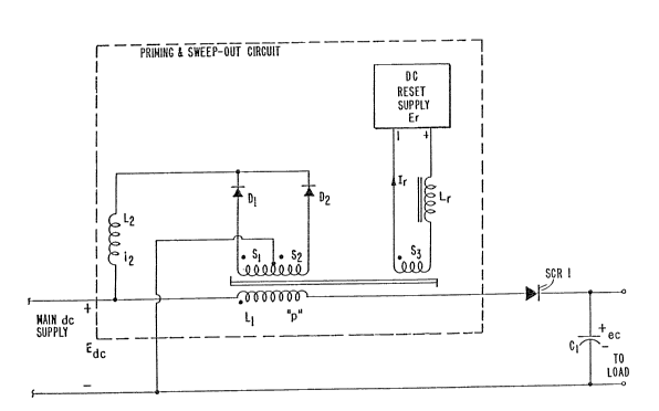
Fig. 1 illustrates a portion of an SCR pulse gen-
erator which utilizes the invention. The pulse generator
employs the well known resonance charging principle
employing a saturable-core inductor Ll to deliver half-
sinusoidal pulses of current from the D.C. power supply
EdC to the capacitor Cl and a load circuit~ labelled
~il 2~S;~:~,15
"LOAD", which may be a resistor, a saturable-magnetic
pulse compressor, another SCR circuit, etc. The satur-
able-core inductor Ll serves as the primary winding "p' of
a transformer the secondary winding Sl-S2 of which is
coupled to the primary and is connected at its terminals
to respective diodes Dl and D2, and from Its intermediate
tap to the - terminal or side of EdC. The common
terminals oE the diodes Dl and D2 are connected through a
storage induc~ance L2 to the ~ side of the D.C. power
9upplY EdC-
The current pulse begins when a series-connected SCR
is gated at tlme ~0, Figs 2C and 2F, and continues for
hal~ a reYonant pariod with t~ ~ ~ seconds, when the
natural oscillation rQverses the direction of current
through SCRl and turns SCRl of~. At turnoff, the positive
voltage ec on the capacitor e~ceeds EdC~ 90 that a n¢t
reverse voltage appears across SCRl. The SCR will regain
its forward voltage-blocking capability aEter a few lO's
of microseconds of reverse bias. Once SCRl has recovered,
the charged capacitor is isolated from the charging
circuits, and its energy can be delivered to the
load.Often, a negative voltage eC`l will remain on C
~i5~3L5
following the discharge inco the load circuit. This
negative voleage adds to the power supply voltage in
driving the natural oscillacion of inductor Ll and Cl when
SCRl is gated. In "lossless" resonant charging, the
capacitor voltage reaches a positive level which is twice
the power supply voltage plus the negative of the residual
capacitor voltage. Thus the peak-to-peak capacitor
voltage during steady-state operation of the pulse
generator may be ~any times the D.C. supply voltage EdC,
shown as 6 ~dc in Fig. 2A. The half-sinusoidal current
pulses pas~in~s through SCRl, Fig. 2C, are correspondingly
lar~e, often reaching thousands of amperes.
The current-carrying and current-~witching capability
of an SCR i9 limited by the ris~ in Junction temperature
caused by reslstive di~ipation. Resistive 1099e~ are
particularly high ~ust after gating when the entire cir-
cuit voltage i9 applied to the small conducting area of
the ~unction near the gate, and at turn off when the
minority carriers stored in the Junction are swept out by
reverse voltage, and the conducting junction area COQ-
tracts to zero. The circuit configuration of Fig. l pro-
vides the designer with a means of reducing the rate-of-
~2~S2:~5
change of SCR current (di/dt) during ehe critical turn-on
and turn-off incervals. The circuit produces a large
increase in the char~ing inductance above ies saturated
value Ll during the two critical intervals, thereby re-
ducing ditdt. At turn-on, the SCR junction is "primed"
with a small ramp of current which e~pands the conducting
junction area prior to the main current pulse. At turn-
off, the SCR current in the reverse direction is similarly
restrained while the reverse circuit voltage "sweeps out"
the minority carriers stored in the conducting ~unction
(see "Timing diagra~", Fig. 2F) The reverse current
terminates very rapidly, and the re3uleing di/dt in the
associated clrcuit inductance causes a transient pulse of
reverse voltage acros~ the now insulating SCR Junction.
The reverse-current restraint provided by the circuit oP
Fig. 1 keeps this translent small, and obviates the need
for prior art serles RC snubber networks across the 5CR
with attendant 1099.
Returning to Fig. 2A illustrating the capacitor vol-
tage ecl following the gating of SC~l, the previous
discharge of Cl through the load reversed its voltage fro~
a positive level of 6EdC to a negative level of -4Ed
~265~ S
similar to that indicated by the dotted line to
the righc. These voltage levels are arbitrary, and serve
only to illustrate the basic law of resonant charging
mentioned above. Another initial condition is the mag-
netic state of the saturable core of inductor Ll. As
indicated by the dots and the polarity or direction of the
reset current Ir in Fig. 1, the core of Ll is fully reset
between discharge cycles from a D.C. reset supply Er con-
neceed through Lr to a reset secondary winding S3 coupled
to Ll as a transfor~er. The reset inductance Lr and the
turns ratios of the windings on Ll ar~ ad~usced such chat
the reset current Ir remains dssentially constant during
the operating cycle to be described. The energy exchange
during SCR priming and sweep-out, which iq the feature of
the invention, occurs acro~s th~ ~aturable core trans-
former windings of Ll -Sl ~ S2 into and out of the rela-
tively smaLl storage lnductor L2, via diodes Dl and D2.
While the core of the saturable inductor is unsaturated,
the wound core behaves like a closely coupled trans-
former. When saturation occurs, the mutual coupling
between primary and secondary windings Ll and Sl-S2
largely disappears.
--8--
Prior to the gate pulse at time t-O, Fig. 2 F, SCRl
has a forward voltage of, say, 5EdC applied co it. When
the gating occurs, the resistance of the SCR junction
collapses almost instantly to nea~ zero, and the 5EdC cir-
cuit voltage transfers to the "p"-turn primary of the
saturable induceor Ll~ Since the core is unsaturated in
the dotted direction (~ig.l) in which the voltage is
applied transformer action occurs to the secondary Sl,
Fig. 2B, across which an induced voltage 5 EdC(sl/p turns
racio) appears. Diode D2 is back-biased, diode Dl is for-
ward-biased, and a n~t voltage (5 (Sl/p) -1) EdC is
applied to the storage indicator L2. Slnce for an induc-
tor the terminal voltage E ~ Ldi/dt, the current is pass-
ing into the pow~r supply through ~econdary Sl, diode D
and L2 will rise at a rat~ givcn by:
di~ ~ I r~ 7 EdC
dt L2 ~P ~
Via the transformer action of the saturable inductor, a
similar rising current (p/Sl) times as large will pass
through the prlmary '-p", SCRl and into the load capacitor.
~2~iS~
As shown in Figs. 2C, 2B and 2D, the linear rises
respectively in the storage inductor current i2 and the
SCR current continue uncil the square-loop core of Ll
saturates abruptly at time tl, Fig. 2F. By design, the
SCR current at the end of the priming interval (O to tl)
is a few tens of amperes small compared to the thousands
of amperes of main-pulse SCR current to follow, bu~ enough
to promote enlargement of the conducting ~unction area in
the SCR. When the core saturates, the mutual coupling
between the primary and secondaries "p" (Ll) -Sl -S2 i5
abruptly reduced, as indicated in Fig. 2B. On the primary
side, all the circuit voltage ~lightly undar SEdC) is
applied to the satura~Qd inductance Ll oE tha primary
winding, and the main-c.Lrcu:Lt sinusoidal re-charge o~ the
load capacitor occurs ovar an lnterval of~ ~ seconds.
Back on the secondary side, at time tl, the main cir-
cuit voltage coupled from the primary nearly disappears,
leaving the (transformed) SCR priming current passing
through the storage inductor L2, the diode Dl, the small
saturated inductance of secondary Sl, and into the power
supply ~dc- This loop current into the power supply falls
~2~
--10--
to zero at a rate of approximately
di2--J - Edc
dt L2
and accomplishes the desired end of returning the (trans-
formed) SCR priming energy stored in L2 to the power
supply. By this design of the saturable inductor Ll, the
pri~ary-to-secondary coupling is small during the satu-
rated interval t1 to t2, Fig. 2F, so that only a minor
amount of the main discharge energy gets diverted into L2,
unllke the action of the circuit of said patent. The
return of priming energy through D, i9 their completed
well beEore the matn discharge t~rminatQs at t2, as shown
in Fig. 2D.
Similar circuit behavior occurs when the main
rq~onant discharge current approaches zaro on its way down
from the pul9e peak. The circuit voltage applied acro~s
the still-saturated primsry Ll oE the saturable inductor
is now negative with respect to the dots (Fig. 1) because
the main-puLse di/dt is negative. Nhen the core of Ll is
pulled out of forward saturation, the entire circuit
voltage (now 6EdC from C1 minu~ EdC from the power supply
,
, I .
~2~5C~S
- 5EdC) appears across the primary of Ll in the negative
direction, Fig. 2B. A currene ramp ineo the power supply
EdC is now initiated on the secondary side via secondary
S2, diode D~ and seOrage induceor L2. The SCR sweep-out
interval starts when ehe primary current goes negative.
So long as there are minoriey carriers remaining in ehe
SCR ~unction, the voltage drop across the SCR remains low,
the rising portion oE the current ramp backwards through
the SCR, and the corresponding secondary current ramp
through D2 persist, Fig. 2E. By design, the core of L
does not saturate in the reset direction beEore the
reverse SCR ~unction curr~nt termlnatea at SCR turn-oEf.
As turn-oEE begin9, the SCR rever~ current tapers rapidly
toward zero, cauaLn~ the primary di/dt in the aaturablq
inductor to go Erom negative back to po~itive. In
responsq, the storage inductor current transEers rapidly
from D2 to Dl at a rate limited by the leakage inductance
between secondaries S2 and Sl, as shown in Figs. 2D and
2E. For a short time, both diodes Dl and D2 conduce at
once, shorting the secondary of Ll. Simultaneously, the
SCR ~unction is rapidly regaining ita reverse vol-
tage-blocking capability, thereby removing the circuit
~2~ 5
-12-
voltage applied to the primary of Ll. The diode Dl and
the storage inductor L2 are left carrying a transformed
replica of the SCR sweep-out current into the power sup-
ply. As in the priming case, this current flow is opposed
by EdC~ and the sweep-out energy is returned to the power
supply. When conduction through Dl ceases, only the reset
current is left applying-magneto ~otive force to the
saturable core. ~s shown in Fig. 2B, at the end of the
secondary voltage waveform, a small relatively long pulse
of voltage occurs as the core i8 reset.
A useful feature of the circuit in Fig. l is that the
two ~econdary windlngs Sl-S2 on the saturable core need
not have the sam~ numbar of turns. A successful circuit
o~ this type, ~or example, has us~d turn~ ratios of 12:5
or the priming circu~t portion and 12:7 for the
~weep-out. Thus the eEfective inductance refQrred to the
primary during SCR priming can be different from that
present during sweep-oue, so that a measure of design
independence e~ists between the peak priming circuit and
the peak sweep-out current. An alternate circuit without
this independenca may use a center-tapped secondary with
Sl ~ S2, or a conventional full-wave four-diode bridge
across a single secondary (not shown).
5~
-l3-
Thus circuit of ~ig. 1 of ehe inveneion has some
common ob~eceives to that of the earlier-mentioned patene
(Fig. 4 ehereof) in (a.) reduction of SCR losses during
turn-on and turn-off by reducing the voltage applied to
the SCR in these critical intervals and tb.) accompl~shing
(a.) with much less dissipative loss than in prior-art
clrcuits with resistors. A collateral advantage is that
of substantial elimination of the reverse-voltage
transient which occurs when SCRl eurns off. The usual
remedy, as be~ore meneioned, i9 a series RC snubber
networks across SCRl, but these burn up a lot of power.
Both circuits, moreover, reduco circuit dildt at turn-off,
ao that the transient volta~Qs, which are proportional to
~l di/dt, are correspondingly less. Thus, among the more
importanC and novel con~ributions of the present invention
snd its new circule are the eliminatlng of one of the
expensive and lossy saturabLe inductors, and the
accomplishing of the return of priming and sweep-out
energy to the power supply immedlately. In the patent
circuit, the reset inductor ~L3) retains the priming
energy through the whole charging Lnterval, causing some
power loss (in R'l). Wieh the present invention, Fig. l,
~265~
the second inductor L2 is but a small and ine~pensive
inductance as is reset induceor Lr7 which advantageously
does not participate in energy e~change or storage, as
earlier e~plained.
Thus, Fig. 1 enables a single, common saturable
inductance network to serve both the priming and sweep-out
circuit needs of the SCR switching charging (or s~orage)
and discharging energy-supply main circuit. If desired, a
pair of such circuits may be used in push-pull, each with
a saturable inductor (transformer) network Ll -Sl-S2 as
above described. Further modifications will also occur to
those skiLled in this art and are considered to ~all
within the spirit and ~cope of ~he inveneion as deEined in
the claim~.