Note: Descriptions are shown in the official language in which they were submitted.
3l6
-- 1 --
POWER AMPLIFIER
BAC~GROUND OF THÆ INVENTION
_ _ _
The present invention relates ~o a power
amplifier which is suitable for use in nonlinear
amplification in high-frequency bands.
Conventionally known as this kind of power
ampliEier is a class "F" amplifier (Tayler, V.J., "A New
~igh Efficiency High Power Amplifier", Marconi Review,
vol. 21, No. 130, pp. 96-109, 3rd Quarter, 19S8, for
example).
To enable the prior art to be described with the
aid of digrams the igures of the drawings will first be
llsted.
Fig. l is a connection diagram showing a
conventional class "F" ampliEier;
Fig. 2A is a diagram showing the waveforms of the
current and voltage at the drain of an FET used in the
ampliEier depicted in Fig. 15
Fig. 2B is a diagram showing the outpu~ waveÇorm
of the power amplifier o the pre~ent inventionJ
Flg. 3 i~ a connectlon diagram illustrating the
convent.~onal cla~ "F" ampliEier adapted for operation in
a very high requency bandS
Fig. 4 is a block diagram illustrating an example
of the power ampliEier oE the present invention which
employs, as a filter means, a band pass filter which passes
therethrough the second harmonic component;
Fig. 5 is a block diagram illustrating the power
amplifier oP the present invention which employs a filter
means adapted to pass therethrough each harmonic component;
Fig. 6 is a block diagram illustrating the power
amplifier of the present invention, for explaining modified
orms of the filter means and a select circuit;
Fig. 7A is a diagram showing a specific operative
example of a band pass filter for use in the present
~s~
-- 2 --
invention;
Fig. 7B is its equivalent circuit diagram;
Fig, 8A is a diagram showing a specific operative
example of a band rejection filter for use in the present
invention;
Fig, 8B is its equivalent circuit diagram;
Fig. 9A is a diagra~ showing a specific operative
example of a low pass filter for use in the present
invention;
Fig. 9B is its equivalent circuit diagram;
Fig, lOA is a diagram showing a specific operative
example of a high pass filter for use in the present
invention;
Fig, lOB is its equivalent circuit diagram;
Fig, 11 i9 a connection diagram illustrating
another example oF the power amplifier oF the present
invention which employs, as the Filter means, a resonance
circuit for the second harmonic component;
Fig. 12 is a blnck ~iagram illustrating an example
in which a plurality oF power ampliFiers oF the present
invention are connected in parallel;
F.ig. 13 is a block diagram illustrating another
example in which a pluraliky oF power amplifiers cf the
present invention are connected in parallel;
Fig. 14 is a graph showing input power V9. output
power and efficiency characteristics of the power amplifier
of the present invention; and
Fig. 15 is a graph showing frequency
characteristics of ~he efficiency and ~- output power
o~ the power;ampli~ier of the present invention.
~265;2~6
-- 3 --
The class "F" amplifier has such an arrangement
as shown in Fig. 1, in which an input signal from an input
terminal 11 is applied to the gate of an FET 12 serving as
an amplifying element and the FET 12 has its source
grounded and its drain connected to a power source terminal
14 via a choke coil 13 which blocks high frequencies. The
drain of the FET 12 is grounded via a filter 15 which
permits the passage therethrough of a second harmonic
component of the input signal and at the same time it is
connected to an output terminal 18 via a filter 16 which
permits the passage therethrough of the fundamental wave
component of the input signal and via an impedance
matching circuit 17.
The FET 12 is supplied with a class "A" or "AB"
bias and generates harmonics of the input signal fed from
the input terminal 11. The Eilter 15 acts as a short-
circuit load for a second harmonic component and as an
open-circuit load ~or a third harmonic ~an odd order
harmonlc) component~ As a result oE thiq, a current i~t),
whiah is sup~rimposition oE th~ undamental and second
harmonic component~ of the input slgnal, ~low~ as indicated
by the solid line ln Fig. ~, and a voltage v~t), which is
a superimpo~ttlon oE the fundamental and third harmonic
componants of the input signal, is created 180 degrees out
oE phase with the current i~t) as indicated by the broken
line in Fig. 2A. The ampliEying operation of the FET 12
is close to a switching operation. An overlap of the
waveforms oE the current i(t) and the voltage v(t) in Fig.
2A is a loss which is dissipated by the FET 12. In this
instance, since the current itt) and the voltage v(t) are
180 degrees out of phase with each other as mentioned
above, the loss is small, and accordingly a high efficiency
can be achieved in the amplifying operation. It is known
in the art that the closer to the half wave of a sine wave
the waveform of the current i(t) is and the closer to a
square wave the waveform of the voltage v(t) is while the
less these waveforms overlap, the more the efficiency is
increased.
2~6
However, since the class "F" amplifier has at
its output a short-circuit load for the second harmonic
component, an increase in the gain of the FET 12 will cause
the second harmonic components of internal electronic
disturbance in the gate of the FET 12 to produce a large
short-circuit current through the filter 15. In practice,
the filter 15 has a certain passing band width, and hence
will allow a larger current flow therethrough caused not
only by the second harmonic component but also by an
electronic disturbance (noise) of frequencies close to that
of the former; therefore, the class "F" amplifier lacks
stability in operation.
Where the class "F" amplifier is employed in a
high-frequency band such as the microwa~e band, the filters
15 and 16 are each formed by a strip line as shown in Fig.
3, and the length oF the filter 15 is specifically selected
to be a quarter of the wavelength of the fundamental wave
of the input ~ignal. The filter 15 is grounded ~ia a DC
blocking condenser 21 and ~he Filter 15 i~ connected to
~ the output terminal 1~ ~ia a DC blocking condenser 22.
Accordingly~ the Filter lS functions, when seen From the
drain terminal oF the FET 12, as an open-circuit load for
the fundamontal wave and as a short-circuit load for the
second harmonic. In practice, however~ it has been
difficu1t, e~en through utilization of such strip line
filters, to obtain a class "F" ampliFier suitable for
operation at frequencies above 1 GHz or so, because the
lengths of the strip lines must become unpractically short.
Moreo~er, since the Filter 15 has to be grounded at one
end through a throuyh-hole to a grounding conductor formed
on the oppcsite surface of a circuit board, complicated
and high precision manufacturing techniques are required
for obtaining the intended filter characteristic. Also
for this reason, the ~lass "F" amplifier i~ not suita~le for
use especially in high-fre~uency bands.
~2~;5~
-- 5
SUMMARY OF THE INVENTION
.
It is therefore an object of the present invention
to provide a power amplifier which is high in efficiency
and stable in operation.
Another object of the present invention is to
provide a power amplifier which is high in efficiency,
stable in operation, and relatively easy to manufacture
for use in particularly high-frequency bands
According to the present invention, the input
signal is divided by a divider into two, and the divider
outputs are applied to first and second amplifying means
for creating their individual harmonics A filter means
is connected across the outputs of the first and second
amplifying means. The filter means includes a filter that
rejects the fundamental frequency component but passes
therethrough the harmonic components of the input signal.
The outputs of the first and second amplifying means are
respectively connected to first and second select circuits
which pass the Fundamental frequency component of the input
signal. The outpu~s from the first and second select
cirouits are combincd at the same amplitude and in phase
with each other.
The power ampliFier according to the invention
also includ~s phHse inversion means which causes
25 ~ an even order harmonic component in the output of either
one af the first and 5econd amplifying means to be 180 de~rees
out of phase with respect to an even order harmonic
component fed thereto from the other one of the amplifying
means via the filter means so as to cancel each other.
In other words, the load viewed from the output side of
each of the first and second ampliFying means constitutes
a short-circuit load for the even order harmonic component;
in this respect, an opera*ion characteristic similar t~ that
of the afore-mentioned class "F" amplifier is performed.
The filter means may include a filter by which an odd order
-- 6 --
harmonic component from the output of either o~e of the
first and second amplifying means and an odd order harmonic
component from the output of the other amplifying means
via the Filter J are rendered equal in phase with each other
at the output side of either of the first and second
ampliFying ~eans. In this case, the load viewed from the
output side of each of the first and second amplifying means
constitutes an open-circuit load for the odd order harmonic
component and the amplifying operation characteristic
becomes further closer to that of the class "F" amplifier.
In addition, since the internal random
dist,urbances of the two amplifying means are independent
of each other, the filter means will not function as
short-circuit loads For the e~en order harmonic components
of the random disturbances. That is, there is no fear of
the ampliEying operation becoming instable. Furthermore,
since the Eilter means is connected across the outputs oE
the first and econd ampliEying means, it is possible to
employ, iE desirQd, an arrangement o the fil~er means
~ that re~uires no through-hole in a circuit board for
connection to ground, and accordingly a power a~plifier
Eor use at particularly high frequencies can be fabricated
relatively easily.
~2~52:~
DESCRIPTION OF T~IE PREFERRED_EMBODIMENTS
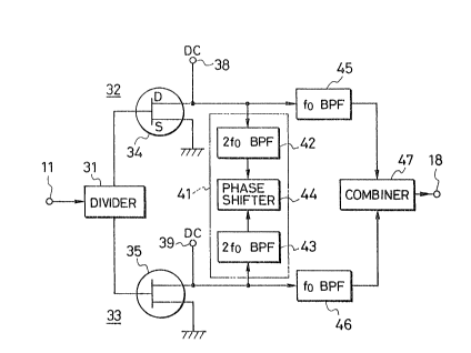
Referring now to Fig. 4, a concrete embodiment
of the present invention will be described. An input signal
from the input terminal 11 is equally divided by a divider
31, for which may be used a 90 hybrid, in-phase hybrid,
or opposite-phase hybrid The divider 31 has its two
output terminals connected to the inputs of first and second
amplifying means 32 and 33, respectively. The first and
second amplifying means 32 and 33 employ, for example, FETs
lû 34 and 35 as amplifying elements. The FETs 34 and 35 have
their gates connected to the two output terminals of the
divider 31, respectively, their sources grounded, and their
drains connected to DC power terminals 38 and 39,
respectively. In order for the first and second amplifying
means 32 and 33 to produce a lot of harmonic components,
the FETs 34 and 35 are each supplied at the yate with a
class IIB'i bias.
The outputs of the first and second amplifying
n~eans 32 and 33, i.e. the drains of the FETs 34 and 35 in
this example, are interconn0cted via a filter mean9 41.
In this example, band pass filters 42 and 43 which inhibit
the passage thHrethrouyh of the Fundamental frequency
component fO of the input si~nal but permit the passage
therethrouyh of its second harmonic component 2fo~ are
connected, as the filter means 41, to the drains of the
FETs 34 and 35, The outputs of the band pass filters 42
and 43 are interconnected via a phase shifter 44. A
variable delay line or variable phase shifter, for instance,
is used as the phase shifter 44.
The drains of the FETs 34 and 35 are also
connected to band pass filters 45 and 46 which serve as
first and second select circuits which pass the fundamental
frequency component fO nf the input signal. The outputs
~s~
of the band pass ~ilters 45 and 46 are connected to two
input terminals of an ln-phase combiner 47, which has its
output terminal connected to the signal output terminal
18. The combiner 47 needs only to combine two inputs in
phase with each other and may be formed by a device which
corresponds to a device used as the divider 31, such as
a 90 hybrid, in~phase hybrid, or opposite-phase hybrid.
The band pass filters 42 and 45 and the drain
of the FET 34 are impedance-matched and the band pass
filters 43 and 46 and the drain of the FET 35 are also
impedance-matched. A current il of the second harmonic
component 2fo flows from the drain of the FET 34 via the
filter means 41 to the drain of the FET 35. Conversely,
a current i2 nf the second harmonic component 2fa flows
from the drain of the FET 35 via the filter means 41 to
the drain of the FET 34. At this time, the voltage of the
second har~onlc component 2Fo Flowing from the drain of
the FET 34 ko the band pass filter 42 and the ~oltage of
the second harmonic oomponent 2fo flowing from the band
pa9s filter 42 to the drain oF the FET 35 are rendered 1
degrees out oF phase with each other at the drain of the
FET 34. Similarly, voltages of the second harmonic
component 2fo from the drain of the FET 35 to the band pass
filter 43 and from the latter to the former are also
rendered opposite in phase to each other at the drain of
the FET 35. The phase shif-ter 44 i~ regulated accordingly.
The FETs 34 and 35 are formed by those of the same
characteristic. The above mentioned phase inversion
capability for the second harmonic components can be
provided to either the band pass filters 42, 43 or the phase
shifter 44 of the filter means 41. In the case where a
9û hybrid is employed as the divider 31, the filter means
41 may not have phase inversion capability because the
~;~6S2~6
g
second harmonic components produced by the FETs 34 and 35
are opposite in phase, providing that the signal paths from
the outputs of the divlder 31 to the gates of the FETs 34
and 35 produce the same amount of phase shift.
With such an arrangement, the input signal from
the input terminal 11 is divided by the divider 31 into
two outputs, which are applied to the first and second
amplifying means 32 and 33 for creating harmonic components.
The second harmonic component 2fo output from the drain
of each of the FETs 34 and 35 is provided via the filter
means 41 to the drain of the other fET without substantial
loss. These harmonic components are equal in amplitude
but opposite in phase, and hence are short-circuited. Third
harmonic components 3fû occurring in the drains of the FETs
34 and 35 are rejected by the band pass filters 42, 43,
45 and 46, and hence are open~circuited. On the other hand,
only the fundam0ntal harmonic components Fo of the input
signal are rejected by the band pass Filtars 42 and 43 but
p0rmitted to pass throu~h the band pass Filters 45 and l~6
and are then combined by the combiner 47 in phase with each
other, and the combined output i~ provided at the output
terminal 1~. That i9~ the power ampliFier oF this
embodiment has khe same operation characteristics as does
the conventional class "F" ampliFier, In the drain oF each
of the FETs 34 and 35, the current i(t) which is a
superimposition of the fundamental and second harmonic
components fO and 2fo on each other flows as indicated by
the solid line in Fig. 2A, that is, just like a half wave
of a sine wave, and the voltage v(t) which is a
superimposition of the fundamental and third harmonic
components fO and 3fO on each other is produced as indicated
by the broken line in Fig. 2A, that is, just lika a square
wave. The input signal is amplified by the FETs 34 and
~2~S2~i
- 10 -
35 in a switching mode, thereby performing power
amplification with a high eFficiency. The amplified output
~oltage available at the output terminal 18 is only the
fundamental harmonic component as shown in Fig. 2B.
The filter means 41 can also be adapted to
effecti~ely act on each harmonic component. As illustrated
in Fig. 5 in which the parts corresponding to those in Fig.
4 are identified by the same reference numerals, a band
pass filter 48 which passes therethrough the third harmonic
lû component 3fû of the'input signal, a phase shifter 49, and
a band pass filter 50 which passes therethrough the third
harmonic component 3fO are connected between the drains
of the FETs 34 and 35, in addition to the provision of the
band pass filters 42 and 43 and the phase shifter ~4 for
the second harmonic ,component 2fo~ The phase shifter 49
i9 regulated so that voltages oF the third harmonic
component 3Fo which flow in and out of the band pass filters
48 and 50 in opposite directions are of the ~ame amplitude
and phase in each of the dralns of the FETs 34 and 35,
Fur~h~rmor~, a ba~d pass ~ er,51 which passes
therethrough a fourth harmonic component ~fû of the input
signal, a phaso shifter 52, and a band pass filter 53 which
passes therethrough the fourth harmonic component 4Fo are
connected between ~he drains of the FETq 34 and 35, The
phase shifter 52 is regulated so that voltages of the fourth
hsrmonic component 4Fo which flow into and out of the band
pass filters 51 and 53 in opposite directions are of the
same ampli-tude but opposite in phase in each of the drains
of the FETs 34 and 35.
In short, the filter means 41 has an arrangement
in which it rejects the fundamental frequency component
fO of the input slgnal but passes therethrough its higher
harmonic components a~nd constitutes a short-circuit loa'd
~6~
11 -
for even order harmonics 2fo~ 4fO, ... and an open-circuit
load for odd order harmonics 3fn~ 5fo~ ..., respectively.
In the above examples of the invention ~and pass
~ilters are emplcyel as the f~lter mea~s 41, but o~ kinds of filters can
also be u~ z:ed. ~or examp:le, as shown in Fïg. 6, a filter
54, a phase shifter 44, and a filter 55 are connected across
the drains of the FETs 34 and 35; in this instance~ band
rejection filters which reject the fundamental frequency
component fO, or high pass filters which have a cutoff
frequency intermediate between fO and 2fc,may also be
employed as the filters 54 and 55. Likewise, the select
circuits which select the fundamental harmonic components
fO for input into the combiner 47 need not be limited
specifically to the band pass filters 45 and 46, but they
may also be formed by band rejection filters which reject
the second harmonic component ZfO, or low pass filters which
have a cutoff frequency intermediate between fO and 2fo~
as indicated by 57 and 58 in Fig 6. In either case, it
i8 possible to insert betwe~n the select circuits 57 and
2a 58 and the combin0r 47 matching circuits 61 and 62 for
matchin9 th~ fundam~nkal harmonic component fO with the
FETs 34 and 35.
The filters 54 and 55 can be formed relatively
easily as RF filters. In the case of forming each of them
as a band pass filter, distribution-coupled strip lines
91, 92 and 93 are connected in a staggered, partly
overlapping ralation and the length of the distribution-
coupled strip line 92 is chosen to be ~9/2 (where ~9 is
the working wavelength on the line) as shown in Fig 7A.
With this arrangement, a component of a frequency vg/~g
twhere ug is the velocity of signal'propagation) is
outputted from the line 93 in response to an input to the
line 91. Fig. 7B shows an equivalent circuit of such a
~2 EiS;~L6
- 12 -
band pass filter~
In the case of forming each of the filters 54
and 55 as a band rejection filter, it is necessary only
to insert, in parallel, a strip line inductor 95 and a strip
line chip capacitor 96 in a strip line 94 as depicted in
Fig. 8A. Letting the inductance of the inductor 95 and
the capacitance of the capacitor 96 be represented by L
and C, respectively, the rejection frequency is around l/~
Fig. 8B shows an equivalent circuit of this band rejeetion
filter.
The fiIters 57 and 58 can also eaeh be formed as a
low pass filter, simply by eonneeting strip line
induetors 97, 98 and 99 in a T-letter shape between input
and output side strip lines and eonneeting a strip line
eapaeitor lOl to the Foot end of the T-shaped eonneetion
as depicted in Fig. 9A. Fig, 9B shows an equivalent eireuit
of this low pass filter.
MorQover, the Filters 57 and 58 ean eaeh be formed
as a high pass fil~r, ~ by eonneeting a ehip eapaeitor
102 between input nncl output side strip lines and eonneeting
a strip lin~ induetor 103 at ono end to khe eonneetion point
and at the other end to a grounding eonduetor line on ~he
opposite su~:kaoe o:E the eireuit l~oard (not shown) through a
through-holq 104 as illustrated in Fig, lOA. Fig. lOB shows
an equivalent eireuik of this high pass filter.
A dielectrie resonator, for example, ean be
employed as the band pass filter whieh passes therethrough
the seeond harmonie component 2fo~ For instanee, as shown
in Fig. 11, the drain of the FET 34 is coupled via the phase
shifter 44 to a dieleetrie resonator 63 whieh resonates at
to the frequeney 2fojand the drain of the FET 35 is eoupled
.directly to the dielectr~c resonator 63. .Dlelectric resona~ors are~
commercially. a:vailable whieh ean be actually employed at
~L2~ $
- 13 _
1 to 40 GHz at present. Accordingly, the power amplifier
of the present invention can easily be designed for
high-freguency operations. Since the band pass filter
composed of a dielectric resonator has a relatively high
Q, the insertion loss of the band pass filter can be made
relatively low and therefore the short-circuiting effect
for the second harmonic component 2fo will be improved.
.
Fig. 11 illustrates a more practical embo~iment
of the power amplifier of the present invention. A DC
blocking condenser 64 and an input matching circuit 65 are
connected between one output terminal of the divider
31 and the gate of the FET 34, and a DC blocking condenser
66 and an input matching circuit 67 are connected between
the other output terminal of the divider 31 and the gate
of the FET ~5. The gates of the FETs ~4 and 35 are
connected via high fr~quancy blûcking choke coils 68 and
69 to gate bia~ source ter~ninals 71 and 72, respectively.
Conn~cted between the drains of the FETs 34 and 35 and the
DC power sourcQs 3a and 39~ respectively, are high freq~ency
blocking chol~ coilJ 73 an~ 74. ~ DC blocking condenser
7S is connocte~ botween the m~tching circuit 61 and
one input terminal of the combiner 47, and a DC blocking
condenser 76 and a phase shifter 75 are connected between
the matching circuit 62 and the other input terminal of
the combiner 47.
While in the above the first and second amplifying
means 32 and 33 are each described as inclu~ing one
amplifying element~ it is also possible to employ a parallel
connection of a plurality of amplifying elements, for
instance, FETs The amplifying elements are not limited
specifically to the FETs but may also be bipolar -transistors
or similar elements. In the embodiments of Figs. 4, 5 and
~5~
- 14 _
6 the filt~rs 42, 43, 4a, 50, 51, 53, 54, 55 are provided
in pairs For the respective harmonic components to achieve
symmetric signal paths on a circuit baard ~his arrangement
is eF~ective to Faci~itate phase-adjustment at the phase
shifter 44 when the power amplifier is designed for
relatively high frequency operation; however, on~ of the
filters in each pair may be omi~ted as shown in the
embodiment of Fig. 11. It should be noted that when the
signal path between the drains of FETs 34 and 35 via the
filter means 41 is contemplated to effect phase-inversion
for the second order harmQnic components, either the phase
shifter 44 or the combination of the filters 42 and 43 (or
54 and 55) may be designed to have the pha~e-inversion
capability. In either case, the pha~e qhifter i9 desired
to be phas~-adjustable. It should also be noted that when
the power amplifler i~ designed to operate at particularily
high ~re~uen~y, the length o~ a signal path strongly
af~ects the pha~e characteristlcs of the signal path and,
the~e~ore, it i~ important that the total phase shift by
the si~nal path lncluding th~ fllter mean~ 41 be adjusted
~uch that at the drain of ei~her one oE the FETs 34 and
35, the p~ase of the second harmonic component emerging
thererom is 180 out o phase with respect to the phase
of the entering second harmonic component from the drain
of the other one of the FETs via the filter means 41.
Once the length of the signal path is suitably adjusted to
satisfy the above re~uirement, the phase shifter 44 can be
dispensed with. In a similar manner, the phase shifters
49 and 52 in Fig. 5 can be dispensed with.
A high voltage output can be obtained by
connecting in parallel a plurality of the power amplifiers
described above. For example, as shown in Fig. 12, the
input signal from the input terminal 11 is divided into
~26~ 6
- 15 -
four or more even number equal signals, which are provided
in pairs to the FETs 34 and 35 of respective pairs. The
filter ~1 and the select filter circuits 57 and 58 are
provided for each pair oF FETs 34 and 35, and the outputs
from the respective select filter circuits 57 and 58 are
combined by the combiner 79 in phase with one another.
In this instance, the filter 41 may also be connected
between adjacent amplifying means as shown in Fig. 13.
It is also possible to connect another filter means between the
first and last stages of the arrangement of the amplifying
means in Fig. 13.
According to the power amplifier of the present
invention described above, disturbances which occur in the
first and second ampliFying means 32 and 33 are random and
second harmonic components ~fO (even order harmonic
components, in general) oF the same magnitude will not be
created in the first and ~ec~nd ampliFying means 32 and
33 at the same tim~; ther~ore the power ampli~ier is ~i
not likely to become unstable but operates stably.
It is possible to employ an arrangement in which
the Filter means 41 need~ only to be connec~ed between the
output sides of ~he first and second ampliFying means and
need not be grounded. Therefore, an amplifier for use at
high frequencies as in the microwave bancl can be fabricated
relativëly easily ~ecause no cirauit b~ throu~h-hole l~-required.
The power amplifier of the present invention
operates in a manner similar to the class "F" amplifier,
as referred to previously, and hence it will achieve a high
efficiency. For example, in a 17ûO MHz band, according
to the power amplifier of the present invention, its output
power Po with respect to its input power Pi is as indicated
by curve 81 in Fig. 14, the drain efficiency, nd ~ Po/PDc
x 100(~6) (where PDC is DC power consumption by the FET 34)
~i5i2~
- 16 -
is as indicated by curve a2, and the power added
Y~ nad (P i)/PDC x lOO(~o) ~ is as indicated
by curve 83, As the input power Pi lncreases, the
harmonic components of the output power increase, and the
efficiencies nd and nad also increase correspondingly.
For instance, when the input power Pi is about 25 dB, the
efficiency ~d is as high as 80o and the efficiency nad is
as high as 7ûo or so.
The output power Po, the drain efficiency nd,
and the power added efficiency ~ad vary with the deviation
of the working frequency from the set center frequency as
indicated by curves 84, 85 and 86 in Fig 15, respectively.
The power amplifier of the present invention can be utilized
satisfactorily in mobile communications and the like over
the band width shown in Fig 15. The efficiency nd is about
75~6 at tho highest in the prior art and 30 to 40~ at the
best in practice; th0r~Fore, it will be seen that the
pres0nt invention aohicves a high ~fFiciency. As a result
of thls, the present invention can be expected to decrease
the volume of the power amplifier around 306 and reduce
its power con~umption nearly 30~ as compared with
conventional pow~r amplifiers Xn addition, the present
inv0ntion can offer power amplifiers oF hiyh eFficiency
unobtainable in the past, over a Frequency range from the
medium wave to microwave bands and for small to large
outputs.
It will be apparent that many modifications and
variations may be effected without departing from the scope
of the novel concepts of the present invention