Note: Descriptions are shown in the official language in which they were submitted.
PHD 85 177 1 14-10-1986
Central exchange
The invention relates to an exchange for the
computer-controlled switching of dlgital time-inter-
leaved data i.ncoming in cyclically repeated frames in
a number of input lines equal to the number of output
lines via a switching matrix, which comprises
- at the input end first cyclically and parallel operated
change-over switches which distribute the input data
of the input lines frame-sequentially and cyclically
over an identical number of input intermediate lines,
- a central stage connected to the input-intermediate
lines and in~luding data stores, in which the data
paths to be switched are determined and which applies
the data to a number of output intermediate lines
equal to the number of input intermediate lines,
- at the output end, second cyclically and parallel
operated change-over switches which di.stribute the
data frame-sequentially, cyclically over the output
lines on which the transmitted data appear.
Such an exchange is disclosed in EP-OS
116 386 and the corresponding publication "IEEE Inter-
national Conference on Comm~ 1984", Volume 1, pages
299-302. Such an exchange behaves as a one-stage swit-
ching matrix in which consequently no path search is
required, and, in addition, is of the non-blocki.ng type.
25 This known principle can also be used for larger numbers
; of channels or input lines. The central stage, that is
to say the actual switching stage, is then a time-swit-
ching stage which includes a one-bit store for each
channel. In addit.ion to these data stores a ].arge number
30 of switches i.s however required, which together represent
quite a considerable cost.
The i.nvention has for its object to provi.de an
exchange of the type defined in the opening paragraph,
~2~5~2~3
PHD ~5 177 -2- 14-10-19~5
the switching stage of which re~uires less cost and
design effort and more specifically can be reali~ed with
comparatively simple, conventional integrated circuits.
According to the invention, this object is
accomplished in that for any combination of the connec-
tions of input lines to input-intermediate lines provided
by the positions of the change-over switches at the input
end an identical combination of connections of output-
intermediate lines to output lines provided by the chan~e-
over switches at the OlltpUt end is avilable, the sequenceof the combinations always being the same, that in the
centre stage for each inp~t-intermediate line a randomly
addressable data store is provided which has a capacity
to store the data of all the input lines during each
frame and stores the data of each one of further frames
of each incoming line~ and that an addressing arrangement
is provided with cyclically repeated drives all the
data stores in the same address sequence but shifted
through one frame, from data store to data store, to
perform connection-dependent write and/or read operations.
The invention is based on the idea that within
a frame period n channels can be switched in a time
stage, n representing the number of channels of a line.
Then, in a time interval of r frame periods, r.n
channels can ~e switched. This re~uires however time
stages whose capacity must be increased by a factor of
r, that is to say rxn memory locations must be available
in both the data store and in the control store con-
trolling the addresses of the data store. Then r frames
of one single line can be exchanged in a data store for
a total of r frames of r different lines, but from
each line only the rth frame is switched~ To enable
switching of all the frames r time stages or data stores
are consequently required, which, not counting a time
shift of the addresses at the input and output ends,
respectively, are addressed in parallel. Thus a data
store of a larger capacity than for the prior art data
switching office is required, but no switches in the
~2~i~22~
PHD 85 177 -3- 14-10-1986
in the actual switchi.ng sta~e, but only the change-
over swit.ches at the input and output ends.
For the parallel addressing operation all the
control stores receive the same address sequences, so
that the switching computer must for each switching
operation switch on~y one address which is the same
for all the control stores, that is to say the switching
exchange behaves for the external world as a sin~le-
stage exchange. For that purpose it is a requirement
that for each position of the parallel-operated chanae-
over switch at the output end where each input line is
always connected to a predetermined input-intermediate
line, there i.s a posi.tion of the chanqe-over switch at
the output end which is also operated in parallel, at
which each one of the output-intermediate lines which
are always associated with one input-intermediate line
or the corresponding central sta~e, respectively, is
connected to the output line correspondinq to the i.nput
line. This can be easily realized in that it must be
possible to apply in a l:l exchan~e all the data on the
input lines in the same sequence to the corresponding
output lines. The positions mutually assigned to each
other, of the change-0~7er switches at the input and
output ends are, for the sake of efficiency, simul-
taneously assumed.
If the structure or the connection of the inputsto the termina~s of the change-over switches themselves
must be identical for the change-over switches at both
the input and output ends, it is efficient to provide
that in one position of the input and output change-over
switches the input lines wi.th the input-intermediate lines
and simultaneously the output-intermediate lines with the
output lines are always interconnected in an inverse
sequence and that the connections in the other positions
are obtained by a parallel shift of the connections in
one position.
This means that in one position the first input
line is, for example, connected to the last input-inter-
,,
~2~;5~2~3
PHD 85 177 -4- 14-10-19~6
mediate line, the second input line to the second ]ast
input-inter~ediate line etc. Thus, a particularly simple
and well laid-out structure is obtained.
For the prior art arrangement an addressing
mode of the switches which there determine the connection
path is described in which a shift register is used. Such
a shift register is also possible in switching exchanges
according to the invention for controllinq the data store
addresses. However, an embodiment of the invention is
characterized in that the addressing arrangement includes
its own control store for each data store and/or the con-
trol stores receive the same sequence of data storage
addresses. As a resu]t thereof the information for the
connecting path to be switched-through is indeed avai]able
as mu]tiple informati~n, namely once for each data store,
but then the data store with its associated control store,
which both operate at a very high rate, can be combined
in one module~ The information to be entered into the
control store for setting-up a new connection needs only
to be conveyed once from the switching computer in common
for all the control stores, so that searching for a path
by the single-stage method is no longer required.
Basically, both sequences of data storage
addresses for writing and reading can be chosen independent-
ly of the connection to be switched-through, it then
beinq necessary for the control store of each data store
to contain both the write addresses and also the read
addresses. In accordance with a further embodiment of the
invention a simple possibility is provided in which of the
two sequences of data storage addresses for writing and
reading one of these sequences is the natural address
sequence of the data store, independent of the connections
to be switched-through, and only the other sequence is
determined by the connection to be switched-through.
The determination of the other address sequences for the
data stores is then unambiguously obtained without any
further measures, without creating a blocking probahility
differing from zero. To produce the natural address se-
~2~iS2Z~
PHD 85 177 -5- 14-10-1986
quences it is parti~ularly efficient to provide that a
control counter is assigned to each data store, which
produces one of the two address sequences, and that the
control counters always count shifted one-frame length
relative to each other. This can easily be obtained in
that the control counters are all provided with the same
counting clock, but from different initial positions,
or start counting at d~fferent starting instants.
Addressing the control store can be effected
in several different manners. As for a cyclic control of
the change-over switches at the input and output ends the
most simple method is to use one common counter, it is
efficient, in accordance with a further embodiment of the
invention, to provide that al] the control stores are
jointly controlled by one address generator and that the
same sequences of data storage addresses, a~ways shifted
through one frame, are applied to these control stores.
This address generator is then the common counter for
controlling the change-over switches. The information to
be entered into the control store for setting-up a new
connection can simultaneously be entered into all the
control stores hy a corresponding address switch, or the
information is applied to all the control stores and is
not entered therein until the addresses valid for each
control store have just been generated, an address com-
parator then being required for each control store.
In accordance with a still further embodiment
of the invention, it is efficient to provide that each
control store is addressed by the associated control
counter and a~l the control stores receive the same se-
quences of data storage addresses in the same control
storage address. Then the shift in the addressing of the
data stores via the correspondingly shifted addressing
of the control stores is obtained by means of the control
counters which count always shifted through one frame
length. The information, that is to say the data store
addressec for setting u~ a new connection is in this
case entered simultaneously in all the control stores in
,:
20104-~158
the same control storage addresses
Accordlng to a broad aspect of the invention there i3
provlded a coMputer-controlled central swltching exchange for
swltching digital time-interleaved data incoming in cyclically
repeated TDM frames on a number of input lines of such exchange to
an equal number of ou~put llnes of such exchange by meahs of a
swi~ching matrix, which exchange comprises:
input change over swltches operating in parallel and which
cyclically switch the data ~rames on each input line of the
exchange frame-sequen~ially over each o~ a number of intermediate
input llnes of sald matrix, the number of ma~rix input lines being
equal to the number of exchange inpu~ lines;
a central switching stage connected to the matrix input lines
and including data stores, such central ~witching stage
distributing the data frames on the matrix input l~nes over an
equal number of matrix intermediate output lines, such
distribution being determined in accordance with the connections
to be established between the exchange input lines and the
exchange output lines; and
output change-over switches operating in parallel and which
cyclically swi~ch the data frames on each of the matrix
intermediate output lines frame-sequen~ially over each of the
output lines of the exchange;
such exchanqe being characterized in that:
(a) the sequence of connec~ions of the exchange input lines
to the matrix intermediate input lines provided by the input
change-over switches is identical to the sequence of connections
,,, ~
~ . ~
20104-8168
of the ma~rix intermediate output lines to the exchange output
lines provided by the output change-over switches;
(b) ~he central switching staye comprises, for each matrix
input line, a randomly addressable data s~ore which, during each
cycle of the input change-over switches, stores in respective
adclresses therein the data frames on all of the exchange input
lines which are connected to such ma~rix input line durlng such
cycle; and
(c) the central switchiny stage fur~her comprises an
addressing arrangement which cyclically addresses all the data
stores in ~he same address sequences but shif$ed by one data frame
ln the ~uccessive data stores, one of such se~uence being for
reading data frames from the da~a stores and another of such
sequences being for writing data frames into the data stores, such
sequences being set in accordance with the connections to be
established between the exchange input lines and the exchange
output lines.
An embodiment of the invention will now be described in
~reater detail, by way of example, with reference to the
accompanying drawing which shows a circuit diagram according to
the invention for a simplified case in which three input lines and
three output lines are used, each of these lines having two
channels. It will however be obvlous tha~ the same principle also
holds for a larger number of lines with a larger number of
channelæ.
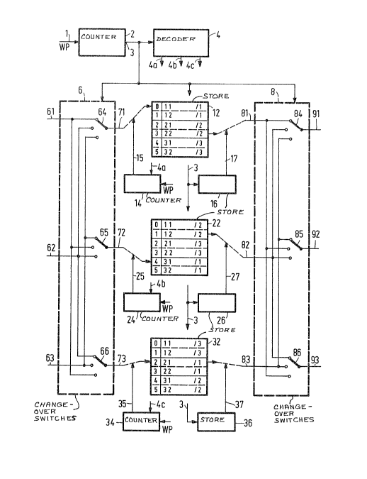
The input lines are denoted by 61, 62 and 63, and it
must be assumed that the data are applied bit-sequentially, that
6a
~2Çi;5~2~
20104-8168
is to say that each channel of each line is represented by a
consecutive sequence of, for example, 8 bits, alternatively
designated as a word. Alway~ L channels or words (in the prezent
example n - 2) form in a conventional manner a multiplex frame.
By ~eans of prior art elements, not shown, the multiplex fra~es
are synchronized with the local frame clock of the switching
of~ice and consequen~ly have mutually equal phases.
The three input lines 61, 62 and 63 are connected to a
change-over arrangement 6, provided at the input end, which
comprises for each input line a change-over switch 64, 65 and 66
each having three positions corresponding to the three input
lines. The output~ of the change-over switches 64, 65 and 66 are
led-out as input-intermediate lines 71, 72 and 73 from the change-
over arrangement 6. All three change-over switches 64, 65 and 66
are switched-through in parallel and consequently connect the
three input lines 61, 62 and 63 in a cyclic sequence to the input-
intermediate lines 71, 72 and 73, that is to say in one position
the input line 61 is connected to the input-intermediate 71, the
input line 62 to the input~intermediate line 73, etc., in the
subsequent position the input line 61 is connected to the input-
intermediate line 72, ~he input line 62 ~o the input-intermediate
71 etc. This results in the sequence of connections shown in the
~ollowing Table 1.
6b
22~3
PHD 85 177 -7- 14-10-1986
Table I
61 71 72 73
62 73 71 72
63 72 73 71
In the last position of the change-over switches
64, 65 and 66 the input lines 61, 62 and 63 are conse-
quently connected in the inverse sequence to the input-
intermediate lines 71, 72 and 73.
o The change-over switches 64, 65 and 66 are con-
trolled vla the output 3 of a counter 2 whi.ch at the
counting input 1 receives a word pulse WP at the start of
each new channel or word on the input lines 61, 62 and
63. In the present case, the counter 2 has a capacity of
two (channel number per input line) times three (number
of input lines) = six posi.tions, so that it effects a
full cycle in three frames whih will be desiqnated super-
fra~es. At each new frame t.he swigches 64, 65 and 66
are incremented one position, so that after a superframe
they have again reached their ori.ginal position.
Each of the input-intermediate 71, 72 and 73 is
connected to the data input of an associated data store
12, 22 and 32 having a number of storage addresses for
alwa.ys one word, the addresses in these data stores
being shown in the lefthand column. Addressing of the
data store 12 is indicated by the broken-line connection
to the i.nput-intermediate line 71 and to the control
connection 15, which originates from a control counter
14 counting the word pulses WP. In addition, the control
counter 14 is reset to its starting position via a line
4a whichoriginates from a decoder 4 which is also con-
nected to the outputs 3 of the counter 2 and at the
beginning of a new frame always produces a signal ~t the
outputs 4a, 4b or 4c. More specifically, the si~nal at
the output 4a is supplied before or at the heginning,
respectively of the first frame of a superframe. In res-
ponse thereto the data word of the first input line of
the first channel of the first frame of a superframe is
~2~i2~
PHD 85 177 -8- 14-10-1986
entered at the address 0 of the data store 12, as
is illustrated by the numbers next to the address ~
in this data store 12. After the subsequent word pulse the
control counter 14 has moved one counting position fur-
ther and, via its connection 15, energizes the address1 of the data counter 12, in which the second channel
of the fi.rst frame of the fi.rst input line 61 is entered.
At the subsequent word pulse the control counter
1.4 is again incremented one position, but, in addition,
the change-over switches 64, 65 and 66 are switched to
their centre positions, so that. the data word of the
second input line 62 from the first channel of the second
frame is entered at the address 2 of t.he data store 12.
Entering data words in the data store 12 is continued in
this way, so that at the end of a superframe the words
; denoted by the numbers in the drawing have been entered.
At the start of the subsequent superframe the information
contained in the data store 12 is always overwritten.
In a corresponding manner the data store 22 is
addressed by a control counter 24 for entering the words
present on the input-intermediate line 72, via the con-
nection 25. This control counter 24 is also incremented
one position at each word pulse WP, but is reset to its
starting positi.on at the beginning of the second frame
2s of a superframe via the input 4b, so that at the beginninq
of a new-superframe it energizes the address 4 of the
data store 22 via the connection 25, as is shown in the
Figure. As the change-over switch 65 connects at the
beginning of each superframe the third input line 63
0 to the input-intermediate line 72, the word of the first
channel of the fir~t frame is entered from the third input
Iine into this address 4. Subsequent thereto, in a
similar way as described for the data store 12, the
words from the input lines are entered in the data store
22, so that finally, as is also the case for the data
store 12, the data store 22 always contains a word from
each channel of each input line, but from a frame dif-
fere~t-t from the frame for data store 12, as wi.ll be obvious
~2~22~
PHD 85 177 -9- 14-10-1986
when the numbers shown next to the addresses are compared
with each other. Also the order of the words concerning
the input lines and the channels therein is identical to
the order oE the words of the data stores l2.
The data store 32 is also controlled for the
writing operation by a control counter 34, via the con-
nection 35, this control counter 34 haviny been reset to
its starting position at the beginning of the third frame
via the line 4c. As a result thereof the control counter
34 addresses at the beginning of a new superframe via
the connection 35 the address 2 of the data store 32,
as is shown in the Figure, and enters therein the word
of the first channel of the first frame of the second
input line 62. At the end of a superframe the data store
32 also contalns a word of each channel of each input
line, but from a frame different from the fra~es for the
other two data stores 12 and 22. In this manner the words
of a~l the three input lines 61, 62 and 63 are stored
during a superframe in all three data stores 12, 22 and
32 from three consecutive frames.
When the data stores 12, 22 and 32 are read,
addressing is only effected via control stores, namely
for data store 12 via the control store 16 and the con-
nection 17, for the data store 22 via the control store
26 and the connection 27 and for the data store 32 via
the control store 36 and the connection 37. In the
example shown here, these control stores 16, 26 and 36
are also addressed via the output 3 of the counter 2.
The content of the control store will be ~escrihed in
detail hereinafter.
The data outputs of the data stores 12, 22 and
32 are now connected to an intermediate-output line 81,
82 or 83, respectively, which represents inputs of a
change-over switch 8 which is of a wholly identical struc-
ture as the change-over arrangement 6, namely incorpora-
ting three -ehange-over switches 84, 85 and 85 which
are controlled in a similar way as in the change-over
arrangement 6 via the output 3 of the counter 2 and connect,
~s~
PHD 85 177 -10- 14-10-1986
for example, the output-intermediate line 81, one after
the other, to the output line 91, thereafter to the output
line 93 and then to the output line 92, and corresponding-
ly also for the other output-intermediate lines 82 and
83. The same sequence of connections as for the change-
over switch arrangement 6 is then ohtained
A detailed description o~ switching-through
the individual connections is given with reference to
the following Table 2.
Table 2
.
Adrr. Adrr. Switched Adrr. Switched Adrr. Switched
3 12 connection 22 connection 32 connection
. . .
15 0 3 22/2 11/4 1 12/2 31/4 2 21/1 21/4
1 4 31/3 12~4 0 11/2 32/4 5 32/2 22/4
2 2 21/2 21/5 3 22/3 11/5 1 12/3 31/5
3 5 32/3 22/5 4 31/4 12/5 0 11/3 32/5
4 1 12/4 31/6 2 21/3 21/6 3 22/4 11/6
20 5 0 11/4 32/6 5 32/4 22/6 4 31/5 12/6
Therein the first co]umn indicates the counter
position occurring at the output 3 of the counter 2 and
which at the same time constitutes the addres~ of the in-
dividual control stores 16, 26 and 36. The next columnindicates the content of the control store 16, which re-
presents the addresses supplied vla the connection 17
for reading the data store 12. The column next to that
defines the switch-through connection, denoted by the
input line number and the channel number and, behind the
stroke, the frame number. This is based on the content,
shown in the Figure, of the data stores 12, 22 and 32
at a predetermined instant, namely at the end of a
superframe comprising three frames, to which the count
of the frame number relates. At the right-hand side of
the third column showing the switched connections, the
frame numbers are counted onwards by 4, 5 and 6, starting
from the instant shown. The sub~acent lines represent to
"
~52~
PHD 85 177 -11- 14-lO-lg36
a certain extent a time axis.
In a similar way the subsequent, fourth column
represents the content of the control store 26, that is
to say the sequence of the addresses driven via the con-
nection 27 on reading of the data store 22~ The thensubsequent solumn indicates the connections which are
switched via the data store 22 in the same way as the
third column. The same holds for the sixth column, which
indicates the content of the con~rol store 26 for address-
ing the data store 32, and the last column shows the con-
nections switched via this data store 32.
At the heginning of the fourth frame after the
situation shown in the Figure, so before the new words
of the input lines, that is to say the first channels
of this fourth frame~ are entered into the data store
12, 22 32, the addressO is then available at the output
3 of the counter 2, and the corresponding control stores
16, 26 and 36 are driven thereby. In response thereto the
data store 12 is read at address 3, and this read word
originating from the second input line from the second
channel of the second frame, is supplied on the first
output line 91 in the first channel of the fourth frame.
Consequently, this word is transferred from the second
input line to the first output line with a delay of two
frames less one channel.
At this instant the control store 26 reads from
the address of the data store 22 the word coming from
the first input line 61 from the second channel of the
second frame, and transfers this word to the third OlltpUt
line 93 in the first channe~ of the frame 4. Here the
delay in the transfer of this word from the input line
to the output line also has a duration of two frame periods
less one channel.
The control store 36 xeads from the address 2
of the data store 32 the word which it has received from
the second input line of the first channel in the first
frame, and this word is supplied on the second output
line 92 in the first channel of the fourth frame. In this
;22~3
PHD 85 177 -12- 14-10-1986
word the switch-through delay from the input liaeto the
output line amounts to three whole frame periods.
After the data stores 12, 22 and 32 have simul-
taneously been read in the manner described above, the
words from the input lines of the first channel in the
fourth frame are entered into addresses determined by the
control counter 14, 24 and 34 and indicated by the arrows
in the Figure. The contents of the data stores has now
changed compared with the representation as regards- the
frame numbers. It should be noted that in the data store
32 information is immediate]y entered again at the same
address 2 from which a reading operation has just been
effected. In the example described this occurs indeed
only at one address, but this may alternatively occur
for each address, determined by the connections, so that
the data stores 12, 22 and 32 must be such that, in the
event of bit-sequential transf~r of the words from the
input lines to the output lines it must be possible
that they are read and also written again at the same
addresses, it alternatively being possikle to reverse
this sequence. For a bit-sequential switch-through it is
in addition necessary for the individual bits of the
words in the data stores 12, 22 and 32 to be individually
addressed one after the other, so that in reading and
writing of each word the bits are nested.
After a complete word has been read and entered
again; the subsequent word pulse WP appears, in response
to which the address 1 for the control stores 16, 26 and
36 appears at the output 3 of the counter 2. With this
address the control store ]6 addresses the address 4 of
the data store J2, as a result of which the word of the
first channel of the third input line of the third frame
is transmitted through the first output line in the
second channel of the fourth frame. This word is conse-
quently only delayed by the duration of a frame plus achannel, which in this example provides the same delay
as for the previously transferred word. Reading the other
data stores is effected in a similar way, also for the
~i5~2~3
PHD 85 177 -13- 14-10-1986
subsequent addresses occurring at the OtltpUt 3 of the
counter 2, where it should be noted that each time after
two addresses not only the change-over switches 64, 65
and 66 but also the change-over switches 84, 85 and 86
always switch one position further~ In addition, for
the further addresses at the output 3 of the counter 2
it should be taken into account that not always the words
shown in the Figure are read from the data stores 12, 22
and 32 but that at the last addresses the words entered
after the instant shown in the drawing, which consequent1y
originate from the respecti~e frames 4 and 5, are read.
In the Table the frame number for these words are under-
lined.
The Table shows that the words of a predefined
channel of a predefined input line are also transferred
to the same output line in the same channel, and indeed
always in the same frame sequence. This also shows that
each channel of each input line can be switched to each
channel of each output line, blocking then not being
ponsible. To that end it is imperative that the individual
control stores always address the associated data store,
shifted through a frame, in the same address sequence
as shown in the Table, as the;address sequence for the
data store 22 is shifted two positions, that is to say
throuqh one frame ]ength downwards relative to the other
sequence of the data store 12, the lower two addresses
in the address sequence for the data stores being added
at top to the address sequence for the data store 2~.
The same holds for the shift of the address sequence of
the data store 32 re]ative to the address sequence of
the data store 22 and, in this approach of the method,
also for the shift of the address ~equence of the data
store 32 relative to the other sequence of the data store
12, so that a looped, cyclic shift is obtained. This is
based on the assumption that the control stores 16, 26
and 36 are all addressed from the output 3 of the counter
2.
A further possibility is to address each control
~2~522~3
PHD 85 177 -14- 14-10-19~6
store from the associated control counter , more specifi-
c~lly the control store 16 from the control counter 14,
the control 26 from the control counter 24 and the control
store 36 from the control counter 34. In these cases all
the control stores have the same contents relative to their
addresses, and shifting the addressing of the data store
during reading is effected by the shifted addressinq of
the control store, fiince the control counters 14, 24
and 34, as described in the foregoing, count after having
been shifted relative to each other. This may be advan-
tageous for entering the connection control information
into the control store from the direction of a switching
computer, not shown, as this computer can then write all
the control stores at the same address. The sequence of
the transmission of words during the switching operation
is not changed then.
So far the description was based on a bit-se-
quential switchin~ of the words. For lines having very high
bit rates the possible switching rates of the change-over
switches 64 to 66 a~nd 85 to 88, and also the operating
rate of the data store and the control stores can be
exceeded. In this case it is then more advantaqeous to
convert in parallel the words of the individual channel
which arrive at the external input lines bit-sequentially
and to switch them bit-parallel in the arrangement shown
and described. The change-over switches 64-66 and 85-86
must then be of a correspondingly multiple construction~
namely one switch for each bitJ and likewise the input
lines 61 to 63, the intermediate lines 71 to 73 and
81 to 83 and also the output lines 91 to 93 must indeed
consist of a number of parallel lines corresponding to
the number of bits per wordO In contrast thereto, no
change is required in the capacity of the data s~ores
12, 22 and 32 and also of the control stores 16, 26 and
36, as in any case all the data stores together must
simultaneously store the word~ of all the input lines of
a number of frames equal to the number of input lines.
The architecture described in the embodiment
22~
PHD 85 177 -15- 1~-10-1986
described in the foregoing as regards the sequence of the
connections effected by the change-over switch and conse-
quently the sequence of the values of the individual
input lines, stored in the data stores, can also be modified,
more specifically such that the input lines 61 to 62 are
connected on a different manner to the individual change-
over switches 64 to 66. The change-over switches 64 to 66
can also be provided inversely, that is to say each input
lines 61 to 63 is connec-ted to a change~over switch. Of
basic importance is that each data ~tore a]ways contains
the same quantity of information from all the input lines
and all the data stores 12, 22 and 32 contain the infor-
mation components of the input lines in mutually the same
sequences also as regards the channels, so that all the
control stores also contain the same sequences of addresses ,
possibly shifted relative to each other, so that these
addresses for setting-up the connection can be uniformly
entered into the control stores. In addition, the con-
nections effected by the change~over switches at the output
end must be matched to those of the change-over switches
at the input end, that is to say always the same com-
binations of connections must be switcheable.
The arrangement described in the foregoing be-
haves as a single-stage switching matrix without internal
blocking. The co~t and design effort required for the
change-over switches is limited, as they can be realized
with conventional, integrated standard modules, part-
cularly in the form of what are commonly referred to as
multiplexers or demultiplexers, whilst customary inte-
grated storage circuits can also be used for the datastores and the control stores. Since the arrangement
behaves as a single-stage switching matrix, no path-
searching facility is required, and each connection is
only determined by one single value, namely an address
which is the same in all the control stores, for the
data stores.