Note: Descriptions are shown in the official language in which they were submitted.
~95~
lS513/703
PEK/KC
09/17/86
1811K
SELF-CHECKING ERROR CORRECTING ENCODER/DECO~ER
This invention relates to data transmission and
storage circuits and, in particular, to encoding and
decoding circuits which encode data to reduce errors.
In high-reliability data processing systems it
is necessary to have circuitry which checks data
that has been transmitted between system units or
which has been stored in system memories and detects
errors which may have been introduced during the
transmission or storage operations. Error detection
and correction is especially necessary in systems in
which data transmission or storage is performed at
high speeds because such systems are mor~ prone to
disturbances by noise and other erroneous signals.
Accordingly, many prior art arrangements have
been developed to protect data stored in memories
and data which is transmitted between data
processing circuits. The simplest of these systems
calculate the "parity" of the data. Generally the
parity of the data is related to the number of
logical "17's in the data word. A data word with an
even number of ones is said to have "even" parity,
lS513/703
PEK/KC
09/17/8
1811~
--2--
while a data word with an odd number of ones is said
to have "odd" parity. A parity bit representing the
parity of the data word (usually the parity bit is a
logical "0" if the parity is even and a logical "1"
if the parity is odd) is calculated from the data
bits and appended to the data word prior to
transmitting or storing the data.
After the data has been retrieved from memory or
received over the transmission channel, the parity
is again calculated from the received data bits and
compared to the retrieved or received parity bit.
If the two are not equal, then it is assumed an
error has occurred and the data can be
re-transmitted or re-retrieved. A problem with this
simple system is that it cannot indicate in which
data bit (or bits) the error occurred, so that the
entire data word must be re-transmitted rather than
~ust the erroneous bit or bits. Accordingly, the
system is slow.
Other, more sophisticated systems have been
developed which are capable of detecting errors in
particular bits and, in some cases correcting the
errors without requiring re-transmission. These
protection arrangements generally operate by
appending to the data a multiple-bit parity code
word which is calculated from the values of the data
bits. One common method of calculating the parity
code word bits is to exclusive-OR the data values in
~6~ 53
lS513/703
PEK/KC
09/17/86
1811K
selected bit positions to generate one bit of the
parity code word. Thus the value of a parity code
word bit will be the parity (number of logical "l"s)
of the selected data bit positions. Both the data
and the appended parity code word are then stored or
transmitted.
After the data has been received over the
transmission channel or has been retrieved from
memory, the code word bits are again calculated from
the retrieved data bits and compared against the
retrieved code word bits. In order to do the
comparison, the re-calculated code word bits and the
retrieved code word bits are combined in
predetermined combinations called "syndromes". The
values of the syndromes are then decoded (compared
to predetermined patterns) to detect whether an
error has occurred. In some systems the syndromes
are further processed to generate error correction
information which is then used to correct erroneous
data bits.
Many prior art error-detecting and correcting
techniques have been devised which are capable of
both detecting and correcting errors which affect
only one data bit. These techniques have met with
varying degrees of success, depending on the
application in which a particular technique is
used. For example, when an error-detecting
technique that is capable of detecting single errors
53
lS513/703
PEK/KC
09/17/86
1811K
is used with random access memories that are
implemented with one-bit-wide memory elements, a
high degree of protection is achieved since the vast
majority of faults that occur in this situation are
single-bit errors. ~owever, when the same technique
is used with a different implementation in which
multiple-bit memory elements are used, the degree of
protection achieved is significantly less since the
probability of multiple simultaneous errors
increases.
Prior art techniques are also available which
can detect or correct double errors or higher
numbers of simultaneous errors. However, the use of
syndromes to correct more than one error requires
complicated circuitry. Consequently the
calculations necessary to generate the syndromes are
lengthy and require complex and expensive
circuitry. Therefore, there is a need for an
error-correcting arran~ement which is relatively
simple and which can at least detect multiple
simultaneous errors~
- ID high-reliability systems another problem
ari~es because the encoding and decoding circuitry
needed to generate the error-correcting codes and to
correct detected errors in the retrieved and coded
information is itself subject to failure. Although
error-correcting encoders and decoders are generally
considered to be more reliable than the memories
~5;~5~
lS513/703
PEK/KC
09/17/86
1811K
they are protecting they are usually considerably
less reliabl~ than the protected memory~ That is,
the probability that the memory produces an error
that is not detectable by the decoder is typically
orders of magnitude less than the probability that
the decoder itself fails. Since a failed
encoding/decoding system which corrects detected
errors can obviously alter the data which it is
supposed to be coding and thereby introduce errors
into the data instead of removing them, prior art
systems which generate undetectable errors are
unacceptable in high reliability data processing
systems.
To ensure that a encoder/decoder cannot fail in
such a way that it generates data containing
undetectable errors it is necessary that it be both
fail safe and self-checking. To be fail safe a
circuit must not itself generate undetectable
errors. That is, if as a result of the failure the
fail-safe circuit erroneously alters one or more
data bits that fact will become apparent to a
receiver of the erroneous dataO A circuit which is
self-checking must, in ordinary usage, exercise all
of its data paths in such a way that, if it does
contain a faulty element, that fault will be
exposed. In a high-reliability system, it is
necessary that the data detection/correction
circuitry be both fail-safe and self-checking.
53
lS513/703
PEK/KC
09/17/86
1811K
- The foregoing objects are achieved and the
foregoing problems are solved in one illustrative
embodiment of the invention in which an
encoder/decoder circuit is constructed in two
identical halYes. Each half of the circuit receives
one half of the total data information, detects
errors in that information and corrects single bit
errors in the data. The circuit half provides
corrected bit outputs and a signal which indicates
whether the data is valid or not.
In particular, each circuit half generate-s "half
syndromes" based on parity code signals generated
from the data available to it and parity code
signals received from the other decoder half. The
error-correcting algorithm and the circuit
implementation is chosen so that a failure in either
circuit half which causes its parity code signals to
be in error cannot force the half syndrome into a
pattern which, in turn, causes an erroneous data
modification without also signalling that the data
is invalid.
More specifically, the parity check code used in
each circuit half is single-error detecting. That
is, any single-bit-error produces a unique set of
syndromes or parity check relationships. Since the
syndromes for each particular error are different
from the syndrome resulting from another single bit
i25~
lS513/703
PEK/KC
09/17/86
1811K
error, the syndromes can be used to generate error
correction information~
In addition, if each data word is broken into
two halves with one half containing the least
significant bits of each byte and the other half
containing the most significant bits of each byte,
the inventive parity check code relationships are
symmetrical with regard to the least significant and
most significant data word halves. The parity check
code also detects all multiple errors affecting data
bits separated from each other by multiples of eight
bit positions. Due to these two facts, the
circuitry which generates and decodes the parity
check relationships can be split into two identical
halves with each half circuit generating and
decoding half of the parity check relationships.
Furthermore, the parity relationships generated in
each half circuit as intermediate variables in the
encoding and decoding process can be combined to
produce byte parity relationships tnat can be used
to protect data sent from the half circuit to
external receivers or to check data received from
external sources.
Figure 1 shows a parity check matrix defining
the parity check relationships used with the
inVentiYe cir~uitry.
33
lS513/703
PEK/KC
09/17/86
1811K
Figure 2 shows a half matrix of the parity check
matrix shown in Figure 1 which defined the parity
check relationships used in each half circuit.
Figure 3 is a block schematic diagram of
encoderjdecoder circuitry constructed in accordance
with the invention.
Figure 4 is a more detailed block schema.ic
diagram of each half of the encoder/decoder
circuitry.
Fig~re 5 is an electrical schematic diagram of
the logic gate array used in one input buffer.
Figure 6 is an electrical schematic diagram of a
logic gate array used in a second input buffer.
Figure 7 is an electrical schematic diagram of
logic gate connections in a first-stage syndrome
generator.
Figure 8 is an electrical schematic diagram of
gate connections in a second-stage syndrome
generator.
Figure 9 is an electrical schematic diagram of
logic gate connections in a ~irst-stage syndrome
decoder.
Figure 10 is an electrical schematic diagram of
logic gatP connections in a second-stage syndrome
decoder.
Figure 11 is an electrical schematic diagram of
logic gate connections in a data corrector circuit.
~26~ 3
lS513/703
PEK/KC
09/17/86
1811K
Figure 12 is an electrical schematic diagram of
logic gate connections in an encoder circuit.
Figure 13 is an electrical schematic diagram of
logic gate connections in a byte parity
encoder/decoder circuit.
Figure 14 is an electrical schematic diagram of
logic gate connections in a byte parity corrector
circuit.
Figure 15 is an electrical schematic diaqram of
logic gate connections in an error condition
detector circuit.
Figure 16 is an electrical schematic diagram of
logic gate connections in the circuitry which
generates a valid data bit signal when the data is
valid.
The inventive encoder/decoder circuitry is based
on a set of parity check relationships which allows
the encoding and decoding circuits to be split into
two halves while maintaining fail-safe and
self-checking propertiesO The particular parity
check relationships used to implement the inventive
encoder/decoder are defined by the parity check
matrix shown in Figure 1. Each row of this matrix
shows the data bits comprising one 32-bit data word
and a corresponding B-bit parity word. The data
words are arranged with the least significant bit
located at the right and the most significant bit
~2~ 3 g
lS513/703
PEK/KC
09/17/86
1811K
--10--
located at the left. The corresponding parity word
is located to the right of the data word with the
least significant bit at the right and the most
significant bit at the left.
Each row of the matrix represents one parity
check relationship. For each row, the data and
parity bit positions marked by "l"s are constrained
to bave an even number of logical "ll's. Thus, for
example, for row 1, bit position 7 of the parity
check word will be a logical "1" if data bit
positions 4, 5, 6, 12, 13, 14, 20, 21, 22, 24, 25,
26, 27, 28, 29 and 30 contain an odd number of
logical "lns. Otherwise, bit position 7 of the
parity check word will be "0"~ Bit positions which
are denoted with a "0" do not enter into the parity
relationship and may be either logical '11"s or "0"s
without affecting the relationship.
Similarly, row 2 of the matrix represents
another parity check relationship in which bit
position 6 of the parity check word will be a
logical "1" if data bit positions 4, 5, 7, 12, 13,
15, 16, 17, 18, 19, 20, 21, 23~ 28, 29 and 31 have
an odd number of logical "l"s, otherwise, bit
position 6 of the parity word will be a logical ll0n.
The set of parity check relationships
illustrated in the matrix of Figure 1 has several
important characteristics. First, it is single
error detecting - all data words containing an error
lS513/703
PEK/KC
Og/17/86
1811K
--11--
in a single bit will be detected - and,
simultaneously, the code is double-error detecting.
This characteristic is a consequence of two facts
(a) that each column of the matrix is different from
all other columns and (b) the term-by-term, modulo-2
sum of any pair of columns is distinct from all
single columns.
Fact (a) ensures that any single-bit error
produces a unique set of parity errors (syndrome).
For example, an error in data bit position 24 will
cause parity errors in the parity relationships in
rows 1, 5, 6 and 7. No error in another bit
position will cause parity errors in that set of
rows. Therefore a syndrome which consists of
correct parity relationships in rows 2-4, and 8 and
erroneous relationships in rows 1 and 5-7 indicates
an error in data bit position 24.
Fact (b) above ensures that any pair of
simultaneous errors results in a syndrome
distinguishable from that resulting from any single
error~
The ability to correct single errors is not
unique and is found in many prior art coding
schemes. The inventive code has several additional
characteristics which are unique and form the basis
of the code's fail-safe and self-checking abilities.
Another important characteristic of the code
shown in Figure 1 is that all multiple errors
lS513/703
PEK/KC
09/17/86
1811K
affecting only data bits confined to a single nyble
or affecting only data bits separated from each
other by multiples of 8 bit-positions are
detectable. For example, the code will detect a
multiple error affecting any subset of the bi~s in
data bit positions 6, 14, 22 and 30. These latter
characteristics follow from the fact that no
term-by-term, modulo-2 sum of any two or more
data-bit columns of the Figure 1 matrix which are
- 10 either confined to the same nyble or are separated
from each other by multiples of 8 is identical to
any single column of the matrix.
Two additional important characteristics of the
code depicted in the Figure 1 matrix allow the code
to be implemented by circuitry constructed in two
identical halves and make the implementation
fail-safe and self-checking. One of these
characteristics is the fact that the Figure 1 matrix
can be split into two identical half matrices with
each half matrix defining four of the eight parity
check relationships. In particular the parity
relationships are established by exclusive-ORing the
- selected data bits to form the parity bit. Since
the exclusive-OR operation is associative (A XOR ~B
XOR C) - (A XOR B) XOR C) and commutative (A XOR B =
B XOR A), the columns of the Figure 1 matrix can be
rearranged without affecting the error correcting
and detecting abilities of the code. In addition,
.,
53
1S513/703
PEK/KC
Og/17/86
1811K
-13-
due to the properties of the exclusive-OR operation,
the parity relationships can be computed in pieces
and later combined to form the complete parity
relationship.
When the columns are rearranged, the matrix can
be split into two identical halves because the
parity check relationships are symmetrical with
respect to half data bytes containing the most
significant bits and the least significant bits.
The split can be performed as follows: The 32
data-bits are divided into four 8-bit bytes which
are arbitrarily assigned the identifiers K, L, M,
and N. Each byte is in turn divided into an "upper"
half-byte or "nyble" (designated by a "U" containing
the most significant bits) and a "lower" half-byte
or "nyble" Idesignated by an "L" containing th~
least significant bits). Thus there are a total of
eight data-bit nybles which are designated by two
letters codes: UK, LK: VL, LL: UM, LM; and UN, LN.
In addition, the parity word is divided into an
upper 4-bit parity nyble (designated as "UP") and a
lower 4-bit parity nyble (designated as "LP"). The
data nyble designations and the parity nyble
designations are shown in Figure 1.
With the foregoinq notation, the parity code
balf matrices assume the form shown in Figure 2. In
figure 2, the designator "X" stands for either "U"
or "L" and the designator "Y" is the "complement" of
,
3.Z~ 3
lS513/703
PEK/KC
09/17/~6
1811K
-14-
;
X (that is, if X stands for l'U" then Y stands for
'IL~ and the converse). The matrix is symmetrical
with respect to the data half-word consisting of the
upper half of bytes K,L,M and N (UK, UL, UM and UN)
and the lower half-word consisting of the lower half
of bytes K,L,M and N (LK, LL, LM and LN).
Therefore, a circuit which uses the parity check
relationships shown in Figure 1 can be constructed
in two halves - each half computing the four
relationships shown in Figure 2.
In accordance with the invention, each
encoder/decoder circuit half need only compute eight
relationships. These include the parity of four
data nybles (UK, UL, UM and UN or LK, LM, LL and LM)
and fo~r other relationships involving selected bits
of the four complementary nybles. Since the matrix
is symmetrical, the same relationships must be
calculated by each half circuit. Thus, the half
circuits can be identical. Figure 2A shows the full
parity check matrix arranged to show the symmetry in
relation to the half data words.
Another characteristic of the inventive parity
code which allows for fail-safe and self-checking
characteristics is that each parity check bit can be
generated solely from the parity of one of the eight
data nybles (UK, LK, UL, LL, UM, LM, UN and LN) and
the values of the data bits in three bit position
sets consisting sf bit positions i, i ~ 8, i ~ 16, i
~S~i3
lS513J703
PEK/KC
Og/17/86
1811K
+ 24 where i is equal to three numbers of the set,
i = 0~ 7~ For example, the parity
relationship in row eight of the parity check matrix
in Figure 1 can be calculated from the nyble parity
of nyble UN and the parity of the data bits in data
bit positions i, i ~ 8, i ~ 16 and i ~ 24 where i =
1,2, and 3. When the matrix is rearranged this
characteristic is retained except that after
rearranging the matrix as shown in Figure 2A, each
parity bit can be calculated from one nyble parity
and the values of data bits in three bit position
sets consisting of bit positions i, i + 4, i ~ 8, i
+ 12 where i = 0,,,4.
This latter characteristic allows for internal
self-checking by using some of the nyble parity bits
generated as intermediate variables in the complete
encoding and decoding process to form an additional
code called the byte parity code. This code is not
stored along with the data as is the parity check
code but is instead sent along with the data when
the data is transferred internally in the system.
Since the byte parity code is generated by a portion
of the same circuitry which generates the error
checking syndromes, this circuitry can be checked by
checking the byte parity codes. This is a key
element in assuring the self-checking properties of
the code.
lS513/703
PEK/XC
09/17/8
1811K
-16-
A hlock schematic diagram of the encoder/decoder
circuitry which uses the code relationships shown in
Figure 2 is shown in schematic form in Figure 3 As
shown, the encoder/decoder is composed of t~o
identical halves 330 and 340.
The circuitry in encoder/decoder halves 330 and
340 can operate in either the encoder mode or the
decoder mode. In Figure 3, the arrows show the data
flow when the circuit is used in the encoder mode.
The encoder mode is used when, for example, data is
being stored in a memory. In the encoding mode the
circuitry generates the parity code bits to be
stored along with the data bits. In addition, in
the encoding mode, the byte parity bits associated
with the data received by the encoding/decoding
circuitry are checked for possible errors.
In the decoder mode the direction of data flow
reverses from that shown in Figure 3 and the decoder
receives code parity bits and generates byte parity
bits. The decoding mode is used when, for example,
data is being retrieved from a memory. In the
decoding mode the retriPved data bits are checked
against the retrieved parity code bits to detect an
error. If a correctable error is detected an
interrupt signal is generated from the circuitry to
inform the remainder of the computer system that a
correctable error has occurred. Each half of the
encoder/decoder circuitry corrects any single error
~Z~ i3
lS513/703
PEK/KC
09/17/~6
1811K
-17-
occurring in the sixteen data bits provided to it
and the corrected 16 data bits are provided on
output buses 360 and 370. Buses 360 and 370 are
combined into output bus 380 and the data thereon is
- 5 provided to thP remainder of the circuitry. When
operating in the decoding mode the circuitry
: generates the byte parity bits to be sent along with
the data and also generates a valid data bit which
-: is sent along with the data. The valid data bit is
used to inform external circuitry when correct and
valid data is on bus 380 or when data which contains
multiple errors that cannot be corrected is on bus
3~.
In particular, in the encoding mode, the data
word and the appended parity code word are provided
to the encoder/decoder circuitry at the left side of
the circuitry via bus 300. In the illustrative
embodiment, each data word has 32 data bits and the
appended parity code word has eight bits~ Bus 300
is s~lit so that sixteen data bits are sent, via
- buses 310 and 320, to each of the encoder/decoder
-! halves 330 and 340. In addition~ one half of the
parity code word consisting of four bits is sent to
each of decoder halves 330 and 340.
- 25 In accordance with the invention, the data and
parity words are split so that the sixteen most
significant data bits (i.e. the four most
significant bits of each of the four bytes) and the
lS513/703
PEK/KC
09/17/86
1811K
four most si~nificant parity code bits are sent to
one of encoder/decoder halves 330 and 340 and the
sixteen 1east significant data bits and the four
least significant parity bits are sent to the other
encoder/decoder half. In addition, four byte parity
bits are provided to the encoder/decoder circuitry.
Two of these bits are provided to each
encoder/decoder half~
Each of encoder/decoder halves 330 and 340
performs calculations on the sixteen data bits and
tbe four parity code bits received from buses 310
and 320. However, to generate the complete parity
check relationships, certain information must be
passed between the encoder/decoder halves 330 and
340 (via bus 350). Specifically, signals passed
between the encoder/decoder halves consist of nyble
parity bits which are generated as intermediate
variables in the encoding/decoding processes.
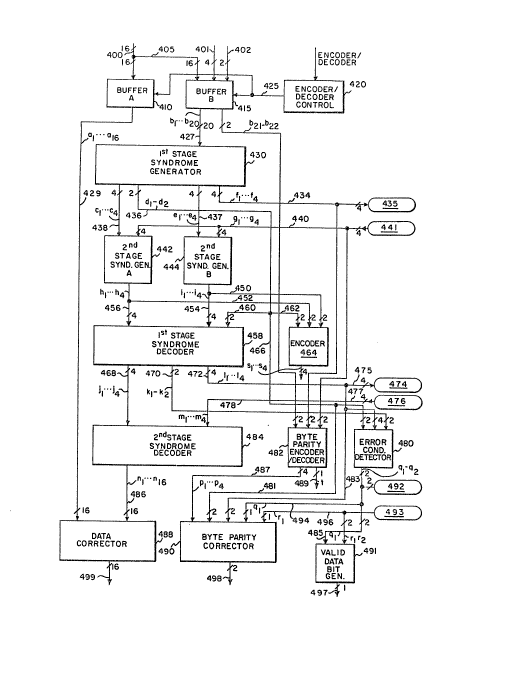
A block schematic diagram of one half of the
illustrative encoder/decoder is shown in Figure 4.
Since each half of the encoder/decoder contains the
same circuitry, only one encoder/decoder circuit
half will be discussed in detail for clarity. It is
to be understood that the other half contains
identical circuitry and operates in an identical
manner on one half of the data bits. Figure 4 shows
the functional relationship between various major
circuit components in the half decoder. The
25~
lS513/703
PEK/KC
09/17/~6
1811K
--19--
circuitry contained in each of the blocks will be
explained in detail hereinafter.
The 16 data bits which are to be processed by
the encoder~decoder circuit half are provided to the
circuit via bus 400 which is connected to the inputs
of buffer 410 and (via bus 405) to buffer 415.
~uffer 415 also receives four parity code bits on
bus 401 and the two byte parity bits on bus 402.
~uffers 410 and 415 contain a plurality of buffer
gates which provide isolation between the
encoder/decoder circuitry and its inputs. They are
under control of encoder/decoder control 420 by
means of ~us 425. Control circuit 420 can enable
either buffer 410 or buffer 415 or both buffers or
disable bo~h buffers in accordance with the specific
operation being performed. When the encoder/decoder
operates in the encoder mode, buffer 410 is disabled
and the four parity code bits received over bus 401
are forced to logical "ons in buffer 415l
Alternatively, when the encoder/decoder circuit
operates in a decoder mode, buffer 410 is enabled
and the two byte parity bits received over bus 402
in buffer 415 are forced to logical "ons.
The output of buffer 410, consisting of 16
buffered data bits (al-al6), is provided, via bus
429, to data corrector circuit 488. If the circuit
is operating in the decoding mode and an error is
detected by the error correction circuitry,
~26~
lS51~J703
PEK/KC
09/17/~6
1811~
-2~-
appropriate correction signals (nl-nl6) will be
provided, via bus 486, to data correction circuitry
488 to cause it to correct the erroneous bit in the
16-bit data word so that the correct 16-bit data
word is applied to output bus 499.
The 16 data bits buffered by buffer 415 (bl-bl6)
are provided, via bus 427, to first stage syndrome
generator 430. In addition, four parity code bits
(bl7-b20) are provided to generator 430. The two
byte parity bits inputs processed by buffer 415
(b21, b22) are provided, via bus 432, to the byte
parity encoder/decoder circuit 482 which will be
described further hereinafter.
The data and parity bit outputs provided from
buffer 415 to first stage syndrome generator 430
Ibl-b20) are combined by the syndrome generator
circuitry to form the eight relationships shown on
the left or right hand sides of Figure 2A.
Specifically, syndrome generator circuitry 430 forms
the four nyble parities ~outputs fl-f4) and the four
other ~arity relationships (outputs cl-c4).
Generator 430 also generates the complements of the
output signals cl-c40 The complementary signals are
designated as signals el-e4 In addition, two other
signals, dl, d2, are generated by generator 430.
These signals are the parity of the half data word
consisting of bits, bl-bl6~ which parity signal is
designated as signal dl and the complement of signal
lS513/703
PEK/KC
09/~7/86
1811K
-21-
dl, signal d2. These latter signals are used in
decoding the syndromes at a later stage as will be
hereinafter explained.
As previously mentioned, the characteristics of
the exclusive-OR operation used to generatP the
parity check relationships or syndrome bits allow
the syndrome bits to be generated in pieces.
However, since each of the encoder/decoder halves
operates on only half of the data bits, each
syndrome bit must be calculated in two pieces and
then later the pieces generated in each half
combined to calculate the complete syndrome bit.
In particular, referring to Figure 2A, in order
to generate each syndrome bit, a parity relationship
shown on the lefthand side of Figure 2A must be
exclusive-ORed with a corresponding parity
relationship shown on the righthand side of Figure
2A and the result exclusive-ORed with the
appropriate parity bit. Since the parity
relationships shown on the left half of Figure 2A
are derived by one circuit half based on one half of
the data bits and the parity relationships shown on
the right half of Figure 2A are derived by the o~her
circuit half baed on one half of the data bits,
information must be passed between circuit halves to
generate each syndrome bit. Illustratively, this
information is the four nyble parities. These
parity signals (fl-f4) are calculated by generator
s;~
lS513/703
PEK~KC
09/17/86
1811K
430 and provided, via bus 434 and terminal 435 to
the other half circuit.
Each circuit half combines the results of the
four parity relationships computed from the data
bits available to it with the four nyble parities
computed by the other half circuit to generate four
syndrome bits (half of the total eight-bit
syndrome). This combination is performed in second
stage syndrome generators 442 and 444. Generator
442 receives four bits, cl-c4, corresponding to the
four co~puted parity relationships calculated from
the input data bits via bus 438 and ~our nyble
parities, gl-g4, received from the other circuit
half over terminal 441 and bus 440. Similarly
generator 444 receives the complemented parity
relationship bits, el-e4, from generator 430 over
bus 437 and the nyble parity bits gl-g4 from the
other decoder halfO Generator 442 generates four
syndrome bits, hl-h4, on bus 456 and generator 444
generates four bits, il-i4, which are the
complements of the bits generated by generator 442.
The complemented bits are provîded on bus 454 to be
used in a later stage of processing.
The nyble parities (fl-f4) generated by
- 25 generator 430 are also provided, via bus 446, to the
byte parity encoder/decoder circuit 48~. The
operation of circuit 482 will be discussed below.
,~ .
~z~
lS513/703
PEK/KC
09/17/86
1811R
-23-
The half syndrome consisting of bits hl-h4 and
its complement (bits il-i4) are used by the first
stage syndrome decoder 45& to detect syndrome bit
patterns which indicate errors in the received data
bits. First stage decoder 458 also receives the
data word parity, dl, and its complement, d2, for
use in this processing. Since each circuit half
operates on only half of the data bits the entire
syndrome cannot be calculated solely by each
circuit. Thus decoder circuit 458 only decodes the
half syndrome bits, hl-h4, provided to it. Decoder
458 generates several sets of output signals. One
set of output signals, jl-j4, indicate the position
of a potentially erroneous bit. However, since the
half circuit does not have the complete syndrome
information at this stage, the signals jl-j4 cannot
specify the exact position of the erroneous bit.
Instead, the signals jl-j4 indicate the modulo-4
position of a potentially erroneous bit.
Specifically, if bit jl is a logical "1", then a bit
in one of the bit positions 4i~1 , i=0,1,2,3 may be
in error: if bit j~=nl" then one of bits 4i+2
i=0,1,2,3 may be in error.
In addition, the first stage syndrome generator
also calculates four bits, 11-14, which indentify a
byte (nyble) in the data half word processed by the
other half encoder/decoder circuit which may contain
a bit that is in error. For example, if bit 11 =
~s~s~
lS513/703
PEK/KC
09/17/86
1811K
-24-
"1" then byte N (consisting of nybles UN and LN) may
contain an erroneous bit. Similarly~ 12 = "1"
indicates that byte M may contain an erroneous bit.
Bit 13 corresponds to byte L and bit 14 corresponds
to byte K. The byte pointer bits, 11-14, are sent
to the other half circuit via buses 472 and 475 and
terminal 474.
The first-stage syndrome decoder also generates
two signals which indicate whether any error has
been detected. In particular, signals kl and k2
identify detected errors. Signal kl="l" indicates
the presence of a detected error (a non-zero
syndromeJ if dl="l". Signal k2=nl" indicates the
presence of a detected error if d2="1".
The error pointers, jl-j4, are provided to the
second stage syndrome generator, 484 via bus 486.
Generator 484 also receives the byte pointer bits,
ml-m4, from the other circuit half via terminal 476
and buses 477 and 478. From these two signal sets
generator 484 has sufficient information to identify
the position of an erroneous bit. Generator 484
produces bit pointers nl-nl6 which identify the
position of an erroneous data bit. Specifically, if
bit nl is "1" then data bit al is erroneous. The
erroneous bit pointers are provided to the data
corrector circuit 488 via bus 486.
As previously mentioned, data corrector circuit
488 receives the buffered data bits, al-al6, from
~l2Ç~S~
lS513/703
PEK/RC
09/17/86
181lK
- buffer 410. The corrector circuit uses the bit
pointer signals, nl-nl6, to effect a correction of
the erroneous data bit. Corrected data bit signals
are provided on bus 499.
The encoder circuit, 464, functions to generate
the parity code word to be appended to the data
before it is stored. It receives the half syndrome
bits, hl-h4, and the inverse half syndrome bits,
il-i4, over buses 452 and 450 respectively. The
encoder circuit also receives the data word parity
signals, dl and d2. The encoder circuit generates
four output signals, sl-s4, which are the bits for
one half of the parity code word. The other half of
the parity code word is generated by the other half
cir~uit.
The error condition detector 480 monitors
internally generated error signals and generates two
outputs, ql and q2. The signal state ql="l"
indicates that an error has been detected. If
signal q2=nln, then the error is either in one of
the data bits belonging to the opposite half circuit
or the error is in one of the parity code bits.
Error condition detector 480 receives the data
parity signals dl and d2 from syndrome generator 430
over bus 466, the byte pointer signals 11-14 over
bus 4B3 from syndrome decoder 458 and the error
signals kl and k2 over bus 470 from decoder 458.
~5~
1S513/703
PEK/KC
09/17/86
1811K
-26-
The byte parity encoder/decoder circuit 482
combines two nyble parity bits generated by the
syndrome generator 430 with two nyble parity bits
generated by the other circuit half to produce two
of the four byte-parity bits. The two bytes used
for calculation of the byte parity are composed of
the nybles XN,YM and XL,YK. In particular~ byte
parity encoder/decoder circuit 482 receives nyble
parity bits fl and f~ over bus 446 from syndrome
generator 430 and nyble parity bits 92 and 94 from
the other half circuit over bus 448. When the byte
parity encoder/decoder circuit is checking the byte
~- parity bits of received data, encoder/decoder 482
........ -e also receives the buffered byte parity bits b21 and
- b22 over bus 432 from buffer 415.
The byte parity encoder/decoder 482 generates
four byte parity signals, pl-p4. Two signals, pl
and p3 are the byte parity signals and the remaining
signals, p2 and p4, are the complements of these
signals. Encoder/decoder 482 also generates an
indicator signal, t, which indicates that the byte
parity of the received data is in error.
The byte parity signals, pl-p4, are sent over
bus 487 to the byte parity corrector circuit~ 490.
This circuit monitors the error signals to determine
whether either of the two bytes associated with the
circuit half contains a correctable error. If so,
the erroneous bit is corrected. In particular, byte
lS513/703
PEK/KC
09/17/86
1811K
-27-
parity corrector 490 receives byte parity signals
pl-p4 from the byte parity encoder/decoder 482 over
bus 487. Corrector 490 also receives byte error
pointers 11-14 and ml-m4 over buses 481 and 483 and
error signals ql and q2 over bus 494. The corrected
byte parity bits are generated on output lead 498.
The valid data bit generator circuit 491
monitors the error signals ql and q2 received over
bus 485 from error condition detector 840 the error
signals rl and r2 (the counterparts of si~nals ql
and q2) received from the other half circuit over
ter~inal ~93 and bus 496. Circuit 491 generates the
valid data bit signal which is sent along with every
word to indicate its validity.
The detailed circuit diagrams for each of the
circuit blocks shown in Figure 4 are shown in
Figures 5-16. In particular, the circuitry for
buffers 410 and 415 is shown in detailed schematic
form in Figures 5 and 6. Buffer 410, as shown in
Figure 5, consists of sixteen NAND gates 500-530.
Each of NAND gates 500-530 has two inputs; one input
receives a data bit from the data half-word assigned
to that half circuit. The other input of each NAND
gate is connected to encoder/decoder control
circuit 420 by means of bus 425. Encoder/decoder
control circuit 420 contains conventional circuitry
which receives commands from the computer system and
places the encoder/decoder circuit into ~ither an
",
lS513/703
PEK/KC
09/17/86
1811K
-28-
encoding mode or a decoding mode. As previously
mentioned, when the encoder/decoder circuitry
operates in an encoding mode, buffer 410 is not
used. Accordingly, control circuit 420 places a
nlow" signal on lead 532, disabling buffer 410. In
order to preserve the fail-safe characteristics,
care must be taken to minimize the possibility of
failures affecting multiple bits. In particularJ as
shown in Figure 5, buffer 410 is implemented with
four-bit-wide integrated circuits. The gates which
handle each bit are selected so that no two bits
belonging to the same data nyble pass through the
same integrated circuit. An illustrative
arrangement of the gates in each integrated circuit
is shown in Figure 5 by the numbers in each NAND
gate. Since there are sixteen NAND gates comprising
buffer 410, four separate integrated circuits each
with four NAND gates are used to implement the
buffer. The circuits are arbitrarily assigned
numbers 1 through 4. The number inside each NAND
gate indicates the integrated circuit to which it
- belongs. If the buffer gates are illustratiYely
arranged in the integrated circuits as shown in
Figure 5, no two bits belonging to the same nyble
will pass through the same circuit.
Figure 6 shows the internal arrangement of
buffer 415, which is arranged in a similar fashion
to buffer 410. In particular, data bits bl-bl6 are
i2S~
lS513/703
PEK/KC
09/17~86
1811K
-29-
buffered through sixteen NAND gates, 600-630. Each
NAND gate has two inputs, one of which receives an
appropriate half data-word bit; the other inputs of
all NAND gates 600-630 are connected together and to
the control circuit 420 via lead 632. This latter
connection allows the control circuit 420 to control
the connection of the encoder/decoder circuit to its
inputs. As with buffer 410, the NAND gates 600-630
are arranged in such a manner so that no two bits
belonging to the same data nyble pass through the
same circuit. Illustratively, NAND gates ~rom four
integrated circuits are used to implement the data
buffer portion of buffer 415. These circuits are
identified as circuits 5-8 and the numbers in each
NAND gate correspond to the circuit assignment.
The four parity code bits, bl7-b20, are also
buffered by NAND gates 632-638 located on a single
integrated circuit (designated as integrated circuit
9~O In a similar fashion, the two byte-parity bits,
b21 and b22, are buffered through two NAND gates,
640 and 642, located on a separate integrated
circuit designated as circuit 10. NAND gates
632-642 are also under control of control circuit
420 by means of control signals on leads 644 and
646, respectively. As previously mentioned, when
the enccder/decoder circuit operates in the encoding
mode, the four parity code bits are forced to
logical "1" by a "low" signal on lead 644 generated
~%~25;~
lS513/703
PE~/KC
09/17/86
1811K
-30-
by control circuit 420. In a similar fashion, when
the encoder/decoder circuit operates in the decoding
mode~ the two byte-parity bits, b21 and b22, are
forced to a logical "1" by control circuit 420 by
means of a "low" signal on lead 646.
The outputs of the data buffer 415 are provided
to the first stage syndrome generator 430 (Figure
4). More specifically, as shown in Figure 7, first
stage syndrome generator 430 consists of a plurality
of exclusive-OR (XOR) gates 702-798. The XOR gates
are connected in groups of four to calculate parity
relationships between selected incoming bits.
In particular, XOR gates 702-724 calculate the
nyble parity signals, fl-f4. As shown in the upper
left quadrant of Figure 2A, the four data nybles are
UR, UL, UM and UN (or LK, LL, LM and LN ) . These
nybles are comprised of data bits bl-b4, b5-b8,
b9-bl2 and bl3-bl6, respectively. XOR gates 702-706
form the nyble parityD fl, o~ nyble UK.
Specifically, bits bl and b2 are XORed together by
- XOR gate 702. Bit~ b3 and b4 are XORed by gate
706. The output of XOR gates 702 and 706 is XORed
by gate 704 to produce nyble parity signal fl = bl
XOR b2 XOR b3 XOR b4. XOR gates 708-712 form nyble
parity f2. Similarly, nyble parities f3 and f4 are
formed by gates 714-718 and 720-724 respectively.
XOR gates 726-758 generate the parity
relationships shown in the lower left quadrant of
lS513/703
PEK/KC
09/17/86
1811K
-31-
I . Figure 2A. One way to generate these relationships
is to XOR the bit signals denoted by nl"s in each
line. However, in order to simplify the circuitry,
reduce the number of gates used and decrease
encoding time, the parity relationships are not
directly generated by XORing the bits designated in
the lower left quadrant of Figure 2A. Instead, the
parity relationships are generated using the
associative property of the XOR operation.
Specifically, the lowest row in the lower left
quadrant can be expressed in terms of the parity of
the entire row as follows:
(b2 XOR b3 XOR b4 XOR b6 XOR b7 XOR b8 XOR blO
XOR bll
XOR bl2 XOR bl4 XOR bl5 XOR bl6) =
( bl XOR ...... XOR bl6) XOR (bl XOR b5 XOR b9 XOR
bl3)
From this relationship it can be seen that the
value of the desired parity relationship can be
obtained from the value of the parity of the entire
data word and the parity of only bits bl, b5, b9,
and bl3. In particular the value of the desired
relationship is equal to the parity of bits bl,b5,b9
and bl3 if the parity of the entire data word is
even; the value of the desired relationship is equal
to the complement of the parity of bits bl,b5,b9 and
~Z~ 5~
lS513/703
PEK/KC
09/17/86
1811X
., .
-32-
bl3 if the parity of the entire data word is odd.
Thus, referring to Figure 7, the first parity
relationship is generated by gates 726-7320
Specifically, XOR gates 726-730 calculate the parity
relationship using incoming data bits bl,b5,b9 and
bl3. Gate 732 XORs the result of the latter
calculation with parity bit hl7 to generate signal
cl, an intermediate variable in the syndrome
calculation. In order to provide for higher
processing speeds, the complement of signal cl is
- calculated by inverting signal cl by means of
inverter 734 to produce the inverted signal, el. At
a later stage in the processing, a choice will be
made between the signal cl and its inversion, el,
depending on the parity of the half data word (dl)
to calculate the entire parity relationship. If
dl="O", d2="1", the signals cl-c4 are "true", if
dl="l", d2=nO" then the signals el-e4 are l'true".
XOR gates 736-764 similarly generate the signals
c2-c4 and their respective inversions, e2-e4. These
signals represent the parity relationships expressed
in the four rows in the lower left quadrant of
Figure 2A.
The first staye syndrome generator also
generates the even and odd parities of the entire
data half-word so that the proper signal of signals
cl-c4 or signals el-e4 can be selected at a later
stage in processing. The even parity relationship
~Z~5~
lS513/703
PEK/XC
09/17/86
1811K
-33-
is generated by gates 766-796. In particular, gates
7~6-768 correspond to gates 702-706 and generate the
nyble parity fl. Gates 772-776 correspond to gates
708-712 and generate nyble parity f2. Similarly,
gates 780-784 generate nyble parity f3 and gates
786-730 generate nyble parity f4. The nyble
parities fl-f4 are combined by gates 778-796 to
generate the parity of the entire data half-word,
dl. Thus dl="0" if the data word parity is even and
dl="l" if the parity is odd. Consequently, if
dl=nl" the parity relationships cl-c4 will be
complemented values, and if dl="0" the parity
relationships cl-c4 will be true values. Inverter
794 ensures that odd parity signal d2 will be the
complement of even parity signal dl. (It will be
noted that the outputs of gates 770, 776, 784 and
790 are identical to those of gates 704, 710, 716
and 722 respectively. The reasons for this
duplication become clear in the ensuing discussion.)
The parity signals cl-c4 and el-e4 are provided
to the second stage syndrome generators 442 and 444.
The second stage syndrome generators 442 and 444
receive the parity outputs, cl-c4 and el-e4, from
the first stage syndrome generator 430 and
' corresponding nyble parities, gl-g4, from the other
half circuit. These signals are combined in the
second stage syndrome generators to produce one half
lS513/703
PE~/KC
09/17/8
lBllK
-34-
of the syndrome bits. The detailed circuitry for
each generator is shown in Figure 8.
In particular, XOR gates 802-808 combine parity
relationships cl-c4 with the nyble parities gl-g4 to
generate the syndrome bits, hl-h4. Each bit
corresponds to the parity relationship in one row of
Figure 2A or to its complement, depending on the
values of the data word parity dl. Therefore, the
four bits, hl-h4, correspond to the four
relationships in the lower half of Figure 2A. The
values of the signals hl-h4 are dependent on the
value of the signals dl and d2 as discussed above.
If dl="l" (d2="0"), then a "low" sisnal in any
syndrome bit indicates an error in the parity
relationship in the corresponding row. For example,
if hl="0" then one of the bits in the lowermost row
marked with a "1" in Figure 2A is in error. By
examining the four syndrome bits, hl-h4 (or their
complements, il-i4) the erroneous bit position can
be narrowed down to one of four positionsO For
example if hl="l" and h2,h3 and h4 - 'l0n then one of
bits bl, b5, b9 or bl3 is erroneous because only
these bits enter into the parity relationships
determining the three syndrome bits, h2, h3 and h4.
In addition, XOR gates 810-816 of the second
stage syndrome generator combines the complemented
parity relationships, el-e4, with the nyble
parities, gl-g4, to generate the complemented
lS513/703
PEK/KC
09/17/86
1811K
-35-
syndrome bits, il-i4.
The parity relationships hl-h4 and il-i4 are
provided to the first stage syndrome decoder 458.
The first stage syndrome decoder compares the half
syndrome bits received from the second stage
syndrome generator to determine whether any data bit
in the sixteen data bits provided to the half
circuit are in error. In addition, the first stage
syndrome generator also determines if any of the 16
data bits processed by the opposite half decoder are
in error cr if any single or multiple bit error has
occurred regardless of location.
The detailed circuitry of the first stage
syndrome decoder is shown in Figure 9. The syndrome
bits hl-h4 and their complements il-i4 are provided
to NAND gates 902-916. These gates check four
patterns of syndrome bits to narrow the position of
any erroneous bit to one of four groups. In
particular, each of the four syndrome bits, hl-h4 is
ANDed with ~he complements o the remaining three
bits. For example, NAND gate 902 generates the
pattern (hl)(i2)(i33(i4) = (hl3(h2*)(h3*)(h4*) where
n*n indicates inversion. This gate will produce a
"low~ output if an error has occurred in one of bits
~5 bl, b5, b9 and bl3 because an error in one of these
bits will produce the syndrome bi~s: hl="l", h2=nO",
h3=nO" and h4="On
In a like manner, NAND gates 904-908 form the
1S513/703
PE~/KC
09/17/86
1811K
three other syndrome patterns. NAND gates 910-916
form four relationships which are the inverse of the
patterns formed by NAND gates 902-908. The output
of NAND gates 902-908 or the outputs of NAND gates
910-916 are transferred to the syndrome decoder
outputs jl-j4 depending on the values of the data
parity bits dl and d2. In particular, if dl="l",
d2="0'l then the outputs of gates 902-908 are
selected. A "high" dl signal is provided to NAND
gate 924. Gate g24 also receives a signal oYer lead
923 from control circuit 420. This signal is ~Ihigh~
when the encoder/decoder circuit is in the decoding
modeO In the decoding mode NAND gate 924 thus
produces a "low" signal on its output which signal
disables AND gates 970, 964, 958, 952, 944, 938, 932
and 926. A "low" d2 signal on is applied to gate
922, disabling it and causing it to apply a ~'high'
signal to gates 928, 934, 940, 946, 950, 956, 962
- and 968. These gates are enabled and transfer the
outputs of gates g02-908 to NGR gates 954-972.
Thus, a nlow" signal at the output of one of gates
902-908 results in a "high" signal at the outputs
jl-j4 of gates 954-972. In addition the outputs of
gates 910-gl8 are transferred to gates 930-948 to
generate signals 11-14. On the other hand, if
dl=n0~ and d2="1~ then the outputs of gates 910-916
are tran~ferred to gates g54-972 and generate the
outputs jl-j4 and the outputs of gates 902-908 are
lS513/703
PEK~KC
09/17/86
181lK
-37-
:1
transferred to gates 930-948 and generate outputs
11-14.
Gates 918 and 920 generate the error detection
bits kl and k2. In particular, if any of the
syndrome bits hl-h4 is "low", indicating that an
error has been detected, gate 918 will be disabled
causing a "high" signal to be produced on its
output, kl. This signal is "true" if dl="l" and
d2="0'l. In a like manner, when dl="0" and d2="1",
if any of the inverted syndrome bits, il-i4, are
Illow", NAND gate 920 will be enabled producing a
"high" signal on its output, k2. Signals kl and k2
are provided to the error detection circuitry 480 as
will be hereinafter described.
Error pointer outputs jl-j4 are sent to the
second stage syndrome decoder 478. ~yte pointer
bits 11-14 are sent to the other encoder/decoder
circuit half. Similarly, byte pointer outputs ml-m4
generated by identical circuitry in the other
encoder/decoder circuit half are provided to the
second stage syndrome decoder 484.
The second stage syndrome decoder 484 is shown
in detail in Figure 10 and combines the error
pointer outputs jl-j4 with the byte pointer signals
ml-m4 to identify the bit position of an erroneous
bit, if any, in the inputs to encoder-/decoder
circuit half.
The second stage syndrome decoder consists of
lS513/703
PEX/KC
09/17/86
1811K
i
-38-
:;
NAND gates 1002-1032. These gates act as a
four-by-four decoder to combine the error pointer
bits jl-j4 with the byte pointer bits ml-m4 to
produce output correction signals, nl-nl6. In
effect the signals ml-m4 select which byte contains
an error and the signals jl-j4 select the position
of the erroneous bit within the selected byte. The
result is a "high" signal on one of outputs nl-nl6
corresponding to the position of the erroneous bit.
Correction outputs nl-nl6 are provided to the data
correction circuit 488.
In order to contain the effect of circuit
failures on the output of the second stage syndrome
decoder, the circuitry is implemented so that no two
outputs corresponding to bits in the same byte
emanate from the same integrated circuit.
Specifically, the numbers inside each of NAND gates
1002-1032 indicates the integrated circuit number to
which the gate is assigned. The circuitry can be
implemented with four integrated circuits, each
consisting of four gat s.
j The detailed circuitry of the data corrector
circuit is shown in Figure 11 and consists of 16
exclusive-OR gates 110Z-1132. Each of XOR gates
1102-1132 combines one of data bits al-al6 with the
corresponding correction signal. If the correction
signal is "high" the corresponding bit is
complemented to produce a corrected output which is
~2~i;2~3
lS513/703
PEK/KC
09/17/86
1811K
-39-
then forwarded to bus 499. The data corrector
circuit is also implemented with four integrated
circuits assigned according to the numbers inside of
each gate.
Figure 12 shows the detailed circuitry for the
encoder 464. As previously mentioned, the encoder
circuitry is used when information is being stored
: in a memory or transmitted as opposed to being read
from the memory or received. The four parity code
signals are generated by four exclusive-OR gates,
1202-1208. Instead of directly using syndrome bits
hl-h4, a combination of bits hl-h4 and il-i4 are
used to produce four signals, two of which are
"true" and two of which are "inverted". This choice
allows the decoding circuitry to check the operation
of both generators 442 and 444 by means of the
code. Specifically, gates 1202 and 1204 process
complemented syndrome bits il and i2 by
exclusive-ORing bits il and i2 with data word parity
bits d2 and dl, respectively. Similarly, gates 1206
: and 1208 process syndrome bits h3 and h4 by
exclusive-ORing them with parity bits dl and d2,
respectively. If dl='71", d2="0" then the parity
code outputs, sl-s4 will be equal to il, i2*, h3*,
h4. Alternatively, if dl="0" and d2=nl" then the
parity code signals, sl-s4 will be equal to il*, i2,
; h3, h4*.
The detailed circuitry of the byte parity
lS~13/703
PEK/KC
09/17/86
1811K
-40-
encoder/decoder is shown in Figure 13. The byte
parity encoder/decoder combines two nyble parity
bits fl and f3 generated by the syndrome generator
located in the same half encoder/decoder with the
two nyble parity bits generated by the syndrome
generator located in the opposite half of
encoder/decoder. The combination yields two of the
four byte parity bits. The bytes for which the
parity signals are generated are composed of nybles
XN, YM and nybles XL, YK as shown in Figure 2. The
byte parity encoder/cecoder circuitry consists of
four XOR gates 1302-1308, two inverters, 1312 and
1314 and one NAND gate 1310. Gates 1302 and 1304
combine the four nyble parity bits fl, f3, g2r 94
corresponding to the aforementioned nybles to
calculate the byte parity outputs pl and p3. Signal
pl is inverted by inverter 1314 to produce
complemented parity signal p2. Similarly, signal p3
is inverted by inverter 1312 to produce complemented
parity signal p4. If the circuit is operating in
the decoding mode these bits are transmitted along
with the data.
If the circuit is operating in the encoding
mode, the calculated byte parities are compared
against the received byte parities. This comparison
is carried out by gates 1306 and 1308 which
exclusive-OR calculated parity signals pl and p3
with the complemented, received byte parity bits on
~2~i52~
lS513/703
PEK/KC
09/17/86
1811K
-41-
leads b21 and b22~ The outputs of gates 1306 and
1308 are provided to gate 1310 which generates a
byte parity error indicator signal, t, for received
data. Signal t is "high" if either gate 1308 or
gate 1306 indicates that one of the calculated
parity bits does not match the corresponding
received parity bit.
The byte correction information, pl-p4, is
provided to the byte parity correction circuitry.
The byte parity correction circuitry monitors the
error signals, ql,rl m2, m4, 11 and 13, to determine
when either of the two bytes associated with the
encoder/decoder half circuit contains a correctable
error. If this found to be the case, the byte
parity correction circuitry complements the byte
parity so that the byte parity will remain correct
after the erroneous bit has been corrected by the
data corrector circuitry.
The circuitry of the byte parity corrector 490
is ~hown in detail on Figure 14. It consists of two
identical halves, each of which generates a
corrected byte parity bit. For example, the
circuitry consisting of gates 1402-1408, 1416-1422
and 1436 generates the byte parity for the byte
consisting of the nyble generated by the local half
decoder and the nyble generated on the opposite half
decoder. The calculated byte parity (pl3 should be
complemented only if both decoder halves detect some
2~3
lS513/703
PEK/KC
09/17/86
1811X
-42-
error (in which case signals ql and rl are both
"low~) and either the local decoder half detects an
error in the nyble associated with the opposite
decoder half (in which case siynal 11 is "high") or
the opposite decoder half detects an error in the
"local" nyble (in which case signal m2 is "highn).
If either of these two situations occur, an error
has been identified as occurring in a data bit of
the byte in question. This is so because if a
single bit error is identified by one decoder half
as belonging to the nyble associated with the
opposite decoder halve, but the error is not
detected by the opposite decoder half, then the
error must be due to a code parity error.
Accordingly, no data bit is in error and the
calculated bit parity should not be complemented.
The gate logic in the righthand half of Figure
14 implements the above error-checking conditions.
In particularg as shown in the righthand side of
Figure 14, the parity bit pl and its complement p2
are combined with the signals ql, rl, 11 and m2 to
generate the output parity bit at gate 1436. Gate
1436 actually complements the output bit, but for
the purposes of this discussion this fact will be
temporarily ignored.
In the situation where both decoder halves
detect some error (ql and rl both "low7') then the
signal ql will be inverted by inverter 1434 to
~l2~2~3
lS513/703
PEK~KC
O9J17/86
1811K
-43-
produce a "high" signal which "high" enables gates
1422 and 1420. Similarly, the "low" rl signal will
be inverted by inverter 1432 to enable gates 1422
and 1420. Gates 1422 and 1420 are provided with the
output of gates 1408 and 1406, respectively. These
gates detect the condition where either of signals
m2 or 11 is "high". This situation occurs when
either the opposite decoder half detects an error in
the "local" nyble N (signal m2 "high") or the local
decoder half detects an error in the opposite
decoder half nyble M (signal 11 "high"). Thus, if
one of these two situations occurs either gate 1406
or gate 1408 will be enabled, allowing the
complemented parity signal p2 to pass through to
enabled gates 1422 or 1420 to output gate 1436.
Alternatively, if either of the error signals ql
or rl is "high", then gates 1420 and 1422 will be
disabled. However, gate 1402, which receives these
latter error signals at its inputs, will produce a
"high" signal enabling gate 1416 which will then
pass the complemented byt~ parity bit pl to the
output gate 1436~ Similarly, if either signal 11 or
signal m2 is "low~, gate 1404 will produce a "high"
output enabling gate 1418 which thereupon passes the
uncomplemented byte parity signal pl.
The left half of the circuitry shown in Figure
14 operates in a similar manner on the byte parity
bit p3 and its complement, p4. As with the right
~2~5;~i53
lS513/703
PEK/KC
09/17/86
1811K
-44-
half of the circuitry, byte parity bit p3 should be
- complemented only if both d~coder halves indicate an
error tql and rl both "lowa') and either the local
decoder half detects an error in opposite half
decoder nyble K (signal 13 "high") or the opposite
: decoder half detects and error in the local nyble L
(signal m4 "high"). If either of these conditions
occurs, then the complemented byte parity bit p4 is
passed through to the output gate 1438. Otherwise,
- - the uncomplemented bit parity byte p3 passes through
one of gates 1424 or 1426 to the output gate 1438.
.. The ql and q2 signals which, respectfully,
indicate that an error has been detected in the
I local and opposite decoder halves are generated by
the circuitry shown in Figure 15 and, particularly,
on the lefthand side of Figure 15.
In particular, gates 1502 and 1504 receive the
data parity bits dl and d2 and the error detection
bits kl and k~ generated by the first stage syndrome
decoder circuitry shown in Figure 9. As explained
- previously in connection with Figure 9, a "high" kl
signal indicates that an error has been detected (if
the data parity byte dl is ~highl' and the data
~: parity byte d2 is "low"). In this condition AN~
gate 1502 will be enabled (due to the "high" error
bit kl and the data parity bit dl being "high").
Gate 1502 will thereupon produce a "high" signal
which, in turn, causes NOR gate 1506 to produce a
,,
~ZÇiS~53
lS513/703
PEK/KC
09/17/86
1811K
-45-
"low" signal on the ql output indicating that an
error has occurred. Alternatively, a true signal on
the k2 error bit (signal k2 I'high''~ and the data
parity bit d2 "high" will enable gate 1504 causing
gate 1506 to, in turn, generate a "low" error signal
ql .
Gate 1510 generates an output signal which
indicates that one of the data bits belonging to the
opposite decoder half contains an error or there is
an error in one of the parity check bits. The q2
signal is generated by gate 1510 from the signals
11-14. These signals point to the byte that
contains an error in a data bit belonging to the
opposite decoder half. If any of the 1 signals is
nhiqh", the q2 signal becomes "low", indicating an
error in the opposite decoder half.
The remaining circuitry shown in Figure 16 is
the valid data bit generator. The valid data bit
generator circuitry consists of gates 1600-1620.
Gate 1620 produces a "highl' signal if the output
data bits are valid, that is, if the retrieved data
and associated parity check bits contained at most
one error (which would have been corrected). Gate
I620 will produce a nlowl' output signal if an
uncorrectable error situation occurs. An
uncorrectable error condition results in three
cases. The first case occurs where both decoder
halves detect an error on the opposite decoder half
~6~i2~3
lS513/703
PEK/KC
09/17/86
1811R
; -46-
~signals q2 and r2 both "low"). The second
condition occurs if an error is detected, but
neither decoder half identifies it as an error
belonging to the other half (signals q2 and r2 both
"high" and either signal ql or signal rl "low").
The third condition occurs if an error is
identified by decoder half as belonging to the
opposite decoder half but the error detected by the
; opposite decoder half is not identified with either
half.
The first two non-correctable error conditions
result in a "low" output signal produced by the
circuitry shown in Figure 16. In particular, under
the first condition where both decoder halves detect
an error on the opposite decoder half signals q2 and
r2 will both be "low". These "low" signals will be
inverted by inverter 1600 and 1602 and applied to
AND gate 1612 enabling the gate to produce a "high"
signal at its output. This "high" signal will be
provided to NOR gate 1620 causing it to produce a
"low" signal at its output indicating that an
uncorrectable error condition has occurred.
Similarly, in the case where an error has been
detected but neither decoder half identifies it as
an error belonging to the other half, the signals q2
and r2 will be "high" enabling AND gates 1610 and
1608. If either of the signals ql or rl is "lowl',
inverters 1604 and 1606 will produce a "high"
,, ~
"
~z~
lS513/703
PEK/KC
09/17/~
1811K
-~7-
signal, respectively enabling either AND gate 1608
or AND gate 1610 to produce a "high" signal. This
"high" signal, in turn, causes NOR gate 1620 to
produce a "low" output indicating an uncorrectable
error condition.
The third uncorrectable error condition will
result in an erroneous bit parity byte. Since
signals ql and rl will both be "low", in accordance
with the circuitry shown in Figure 14 and discussed
above, one of the byte parity`bits will be
complemented even though no data bit is
complemented. Thus, in all cases the uncorrectable
error results in either a "low" data valid signal or
and at least one invalid bit parity byte.
~lith the above described circuit construction,
all failures which cause data to be erroneously
modified during a decoding operation are guaranteed
either to cause the valid-data bit signal to be
- inhibited or to produce at least one erroneous byte
parity bit thus ensuring that th~ error will be
~ instanteously detPctable at the destination. Any
decoder failure not resulting in erroneously
modified data, neverth~less results in either one or
more byte parity errors, an inhibited data-valid
: 25 bit, or an interrupt due to somP detected error
condition which can be used to initiate a diagnostic
routine.
Error detection will occur even when the first
;i3
lS513/703
PEK/KC
o9/17
1811K
-48-
manifestation of the failure occurs during an
encoding operation even if the consequently
improperly encoded data i8 subsequently retrieved
and decoded using the same failed component.
Moreover~ failure detection is not dependent on the
type of failure mode. The circuit retains both
fail-safe and self-checking properties regardless of
any failure, whatsoever~ affecting any component
used to implement the encoder/decoder circuitry.
For example, if an integrated circuit fails, `it is
not reasonable to assume that the failure affects
only one output or that the affected outputs are, as
a result of the failure, permanently driven to a
particular state, such as a logical 1l0ll or a logical
"1". In addition, it is not realistic to assume
that only outputs are affected. An integrated
circuit may fail in such a way that it affects both
inputs and outputs in non-predictable ways.
However, regardless of the manner of failure, the
above circuitry will provide an error indication.
The following Table I indicates the manner of
detecting various failures and components in this
circuitry which are manifest on a decoding
operation. The last column indicates additional
notes which are applicable to each condition. These
notes follow tables I and II.
lS513/703
PEK/KC
09/17/86
1811X
-49-
:,
Table I
Faults first made manifest on a read
Failed Failure No. of Detection Notes
component Mode erroneous Mechanism
Location output data
bits
_
Buffer A Same single None Correctable Note 1
or B bit error in error interrupt
both A & B
outputs
Single bit- Up to four One or more Note
error on B byte-parity
output; other violations
than an iden
: 15 -titical error
- on the A output
No errors on Up to four One or more Note
B output; one byte parity
or more A violations
output errors
~Z'$~ ;3
lS513/703
PEK/KC
09/17/86
1811K
-50-
Multiple bit Up to four One or more Notes 2
errors on B byte parity & 3
output; arbi- violations
trary A output
errors
lst-stage Arbitrary None Correctable Note 4
synarome failure error inter-
generator mode with rupt or inhi-
zero, two or bited valid-
four nyble- data bit
parity errors
Arbitrary None,one One or three Notes 4
failure mode or four byte parity & 6
with 1 or 3 errors; cor-
nyble parity rectable error
interrupt
errors or inhibited
salid data
bit
2nd stage Arbitrary None Correctable
syndrome error inter- Note 5
generator rupt or inhib-
ited va~id-data bit
25*~3
lS513/7~3
: PEK/KC
09/17/86
; 1811~
-51-
1st stage Arbitrary None Correctable Note 5
: syndrome error-inter
decoder or inhib-
ited valid data bit
2nd stage Arbitrary Up to four Up to 4 byte Note 2
syndrome byte parity
decoder errors
. -
D~a - Arbitrary Up to four Up to 4 byte Note 2
corrector byte parity
errors
Encoder Arbitrary None Correctable Note 5
error inter-
rupt or inhib-
ited valid
data-bit
Byte Arbitrary but None Possible byte Note 5
parity with si~nals parity error; & 7
encoder dl ~ d2 not correctable error
both forced interrupt or in-
~ active hibited valid-
data bit
Arbitrary but None Possible byte Notes
53
lS513/703
PEK/KC
09/17/86
1811K
-52-
forcing 2 or parity error: 5 & 7
four nyble-parity inhibited valid-
errors (fl,g2,f3,g4~ data bit
Arbitrary but Four At least 2 byte Note 6
with signals parity errors;
dl~ & d2 inhibited valid-
both forced data bit
active
- and with 1 nyble
parity error (fl,f3)
Error Arbitrary None Up to 2 byte Note 5
-~condition parity errors;
detector correctable error
interrupt or inhibited
valid~data bit
Byte Arbitrary None Up to 2 byte
parity parity errors; possi-
corrector bly inhibited
valid-data bit
Valid data Arbitrary None Possible Note 5
bit correctable error
generator interrupt or
lS513/703
PEK/KC
09/17/86
1811K
.j .
-53-
i
inhibited
;` valid-data bit
The following Table II indicates the manner of detecting
various failures and components in this circuitry which are
manifest on an encoding operation. The last column indicates
additional notes which are applicable to each condition.
These notes follow Table II.
Table II
Failed Failure Mode Detection Mechanism Notes
Component
Location
Buffer B Arbitrary Byte-parity error Note 2
interrupt
1st stage Arbitrary Correctable error Notes 6
syndrome failure interrupt or an ~ 8
mode affect- inhibited valid-
ing only 2nd data bit on a read
stage syndrome
generator inputs
3i 2~ f
1~513/703
PEX/KC
09/17/86
181lK
. -54-
?
All other Byte-parity-error
failure interrupts
modes
2nd stage Failure mode Correctable-error Note 9
syndrome not affecting interrupt or inhibited
the nyble- valid-data bit on a
parity inputs read
from the
opposite
decoder half
All other Byte-parity error
failure interrupt
modes
Encoder Failure modes Correctable-error Note 9
either not interrupt or inhibi-
affecting or ~ed valid-data bit
complementing on a read
both of the
inputs from
the lst-stage
syndrome
generator
lS513/703
PEK/KC
09/17/86
1811~
All other Byte-parity error
failure modes interrupt
Notes applicable to the foregoing Tables I and II.
1. This condition is equivalent to the case in which the
memory output contains a single-bit error, the decoder
corrects the error and initiates an interrupt to announce
that event.
;
2. Buffers A and B, the second-stage syndrome decoder and
the data corrector are all so partitioned that no two
bits belonging to the same byte have any component in
common. Thus, no single-component failure in these
elements can affect more than one bit in any one byte,
(Buffer A is not used on writes, since no error
correction is at~empted in this case.)
3~ The code has the property that all multiple-bit errors
affecting only bits separated by integer multiples of
eight bits are recognized as uncorrectable.
.,
' 4. No data bits will be "corrected" unless the half syndrome
calculated in the non-defective half of the decoder
- 20 contains either one or three logical "lns. Since it is
assumed that the decoder input contains no errors and
that only one of the decoder halves contains a defective
2~3
lS513/703
PE~/KC
09/17~86
1811K
-56-
component, no data bits will be altered uniess either one
or three of the nyble-parity bits ~fl, f2, f3, f4 in
Figure 4) passed from the defective to the non-defective
half are in error.
5. Correctable error interru~ts will occur without any data
bits actually being corrected when the decoder determines
that a sin~le code parity bit is in error.
6. The first stage syndrome generator outputs el-e4 are
normally the complements of outputs cl-c4, and data
half-word parity output, dl, is normally the complement
of output d2. A single-component failure can alter at
msst one of these relationships. Thus, if the
first-stage syndrome decoder is functioning properly,
none of the signals jl-j4 can be active unless either
signals dl and kl, are both "1" or d2 and k2 are both
"ln. Consequently, the byte-parity corrector circuits
are all also functioning and no data "error" can be
corrected without also causing a byte-parity bit to be
complemented if the byte parity was in error prior to
the "correctionn, it remains in error afterwards as
well. Since, under the aforementioned conditions, no
correction can take place unless at least one of the
nyble-parity bits (fl, f2, f3, f4) is in error, data
modifications caused by a first-stage syndrome generator
malfunction must leave at least one byte-parity bit in
lS513/703
PEK/KC
Og/17/86
1811K
-57-
error. (This is true even when the failure leaves dl and
d2 both "1", thereby allowing the possibility that four
data bits are simultaneously modified. In this event all
four byte parities will also be complemented and three
will be left in error, regardless of whether the
correction takes place in the defective or in the
non-defective half of the decoder.)
7. Since the byte parity encoder can affect only two
outgoing nyble-parity bits (signals fl, and f3 in Figure
4~ and two incoming nyble-parity bits (signals g2, g4),
it can not by itself force a correctable error syndrome
(a syndrome having three logical "l"s from one decoder
half and one logical "1" from the other half). If it
forces both dl, and d2 to "1", however, and forces
exactly one error in the outgoing nyble parity bits, it
will cause four bits to be complPmented in the byte
corresponding to the erroneous nyble parity. However,
this will also cause the two byte parities in the
opposite half decoder to be complemented (according to
2~ Note 5) thus creating at least two byte parity errors and
preventing the valid data bit from being set, regardless
of the output of the defective byte parity encoder.
8. Since first-stage syndrome generator failures can affect
at most one pair of outputs cl-c4 and outputs el-e4
(according to Note 6~, such failures can alter at most
one code parity bit. Since the corresponding svn~r~m~ i t
2~3
lS513/703
PEK/KC
09/17/86
lallK
-58-
is calculated (on decoding operations) using the same
defective component, it may or may not be correct
depending both on the failure mode and on the data
pattern~ If the failure is such that tbe calculated
syndrome bit is llO" regardless of the data pattern, no
error will be detected on a read unless a bit error is
actually present either because of some other failure or
- due to a diagnostic test. The effect of such a failure,
however, is to convert a correctable data error syndrome
- into an uncorrectable one (i.e. to change a syndrome
having four logical "l"s to one having three logical
nl"s), thus inhibiting the valid data bit. If the
failure is such that the calculated syndrome bit is
either always a "1" or is pattern sensitive, the effect
is to convert an all "O"s syndrome into a syndrome
identifying a parity bit as being in error ~i.e. into a
syndrome having exactly one logic "1"). In neither case
is incorrect data ever produced.
9O Second-stage syndrome generators A and B each affect only
two code bits, but neither of them can by itself
determine all four half-syndrome bits. Thus, failures in
either one of these units are detected on reads in which
the other is used. Similarly, the encoder can affect
only outputs hl and h2 from buffer A and outputs i3 and
i4 from buffer B. Yet an error in one of the encoder
outputs sl-s4 affects both second-stage syndrome
~iS;;~3
lS513/70
PEK/KC
09/17/86
1811~
-59-
generatoz bits hl-h4 and il-i4 when the improperly
encoded word is read so encoder failures are also
detected on subsequent reads.