Note: Descriptions are shown in the official language in which they were submitted.
5S~
The present invention relates to digital speech
and data transmission on a subscriber's line and more par-
ticularly to improvements in echo cancellers for bidirec-
tional digital transmission systems.
A significant development in integrated service
digital networks ~ISDN) is the 144 kbit/s transmission
technique used for subscriber access to ensure a low error
rate and a small high frequency spectral content so as to
avoid crosstalk. It should be compatible with high
fidelity distribution systems and allow integration of the
whole system so as to reduce cost and increase
reliability.
One of the main problems encountered in echo-
cancellation transmission techniques is in ensuring an
adequate useful signal/residual-echo (S/N) ratio of at
least 20-25 dB, so as to allow correct reception. This
S/N ratio is particularly difficult to obtain when the
system is specified for a maximum 40 dB line attenuation.
Since hybrid matching losses to the line seldom better 10
dB, echo suppression of at least 50 55 dB is necessary to
obtain a satisfactory S/N ratio.
Echo estimation and cancellation are generally
performed by a transverse or memory type structure which
can ensure the desired accuracy in the samples on which it
operates. Memory structures can recover even from non-
linear distortions present in transmission and reception
circuits, while the transverse structures are most useful
for cancelling echoes which do not occasion that type oE
distortion, since they re~uire le99 complex clrcuits.
'rO attain global cancellation values of 50-55
dB, it is however necessary to estimate and cancel the
echo on a very large number of samples, since the tail of
the echo response extends over a very long time interval.
The use of transverse or memory cancellers in such circum-
stances typically requires operation on 25-35 samples,
which entails, besides increased circuit complexity, a
considerably increased processing speed, which hinders
_ 1 _
~;~65~;9~
system implementation in CMOS technology. Currently, CMOS
technology is the best suited to meet requirements such as
low consumption and high integration density, which are
necessary for effective ISDN development.
The present invention seeks to provide an
improved echo cancellation system, which can allow the
attainment of a 50-55 ds signal-to-residual echo ratio
required in worst case conditions. The invention, which
relies for its operation on the behaviour of the echo-
channel pulse-response, allows considerable circuit
simplification as compared with memory or transverse type
cancellers of the same performance, without increasing
internal operation speed. This simplification also
simplifies implementation of the system as an integrated
circuit.
According to the invention, there is provided an
echo canceller for bidirectional digital transmission
systems which cancels the echo tails of a desired number N
of digital symbols transmitted on a line in the next
preceding N signalling periods, comprising means to effect
a summation of the last N transmitted signals, means to
determine an estimated sample of an echo channel pulse
response, and means to multiply the results by one another
to obtain an estimated echo signal for cancelling the echo
tails.
The invention extends to a method of echo
cancellation in bidirectional digital transmission
systems, wherein an echo signal ~k to be used in a period
for cancellation of effects due to a quasi-linearly
decreasing tail of a pulse response of the echo channel of
the system is calculated according to the relationship
ek = hk ~ bk-i ( 1 )
wherein hk is an estimated sample of the pulse response of
the echo channel, bk, bk_1 ... bk_N are logic symbols
transmitted during N preceding signalling periods whose
~2~iS~;i9~
echo tails are to be cancelled, and hk is estimated using
the following relationship:
! ~ k- ~ sgn ~ek_l - ek ~ D
wherein ek_l is the echo signal received in period k-l, D
is a coefficient less than 1 such as to ensure conver-
gence, sgn is the sign extraction functionl and expression
(2) is evaluated by successive incrementation or decremen-
tation of preceding results as a function of the logical
level of bk and bk-N
The foregoing and other features of the present
invention will be apparent from the following description
of an exemplary embodiment with reference to the accom-
panying drawings, in which:
Fig. 1 shows the pulse response of a transmis-
sion channel;
Fig. 2 is a block diagram of a circuit embodying
the invention; and
Fig. 3 shows the pulse response of a transmis-
sion channel with and without the circuit provided by the
invention.
It is known that the echo-channel pulse response
of a connection, after an initial extremely irregular and
variable phase, which is a function of hybrid unbalance,
of line type and of connection topology, exhibits in its
final phase a quasi-linearly decreasing tail. Fig. 1,
which is a composite plot of the response of various
configurations of cable subscriber's line and connection
topology, shows the amplitude oE the echo response as a
function of time, subdlvided into signalling periods. The
form of the pulse response tail is not line dependent tin
fact the Figure includes the case of a channel consisting
of a resistive termination), but depends solely upon the
characteristics of the hybrid transformer. It will
-- 3
~655~4
however, be noted from Figure 1 that the amplitude of the
tail is still at a level such as requires its cancellation
in order to obtain desirable levels of residual-echo-to-
signal ratio. Although the form of the tail depends on
the hybrid transformer, it is still a random variable, due
to the characteristics of the hybrid itself. These
characteristics can vary both due to manufacturing
tolerances or changes in the materials used. It is thus
necessary to use an adaptive technique for their
estimation and cancellation.
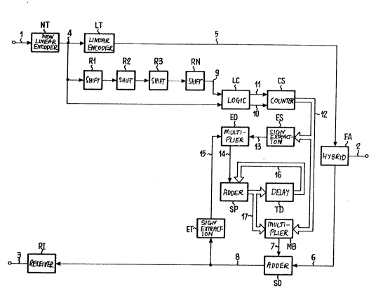
Referring to Figure 2, which shows a bidirec-
tional digital transmission system, a binary signal to be
transmitted on transmission line 2 arrives on line 1, and
received signals are output on line 3. A transmitter is
represented as subdivided into two blocks NT and LT, in
which the linear and non-linear line encoding ~unctions
are carried out. Encoding is generally based on a three-
level code of AMI type. The non-linear function is a
precoding whose aim is to avoid error propagation. Since
the linear encoding effected by block LT is a differential
encoding, an erroneous decision in the interpretation of a
binary signal would cause the transmission of successive
erroneous signals~
At the output of block NT on line 4, a signal
linearly related to the signal applied to the line 2 is
available, which can thus be used to estimate the echo
signal to be cancelled. The output signal from block LT
reaches a hybrid transformer FA on line 5.
Incoming signals from the line 2 and an echo-
signal of the local transmitter formed by blocks NT-LT
pass through the hybrid FA to an input of adder S0 on line
6. The other input Oe the adder receives an estimated
echo signal on line 7, which is locally generated with a
sign opposite to the echo signal received on line 6. An
echo-cancelled useful signal is thus obtained at the
output of the adder on line 8 and 13 sent to a receiver RI
to be decoded and output on line 3.
~2~559~L
An echo signal ek to be used for cancellation of
the tail of the echo response is estimated at instant k.
It is calculated as a product of an estimated sample hk of
the pulse response of the echo channel, and the summation
of symbols bk, bk_1 ... bk_N transmitted during N
preceding signalling periods, whose echo tails are to be
cancelled, the relationship being as follows:
êk = hk ~ bk-i ( 1 )
The value of hk is estimated in an adaptive
manner so that the system can be matched to hybrids having
different characteristics. By using the sign iterative
stochastic algorithm, the following relationship is
obtained:
h = h + sgn ( ~ bk_l) sgn (ek-l - ek_~ D (2)
where ek_1 is the echo signal received at instant k-l, D
is an appropriate coefficient lower than 1 such as to
ensure convergence, and sgn is the sign extracting
function.
It should be noted that the argument of the
first function sgn in the relationship (2) is equal to the
second factor of the relationship (1). In the present
case, this summation is not calculated by executing N
additions every signalling period, but by simply
incrementing or decrementing the preceding result as a
function of the logic level of the binary signal presently
transmitted, bk, and of that of the binary signal
transmitted N signalling periods before, bk_N.
To this end, precoded signal bk, present on line
4, is sent both to a shift register consisting of N cells
Rl, R2, R3...RN, where N is the duration, expressed in
signalling periods, of the pulse response of the echo to
be cancelled, and to a logic circuit LC. At the other
~6~5~4
input of circuit LC, signal bk_N is present on line 9
from the last cell RN of the shift register. The signals
at the outputs of the circuit, connected to lines 10 and
11 are related to those at the input as follows:
bk bk-N 10 11
O 0
0 1 0 0
0 0
The signals on lines 10 and 11 are used to con-
trol an up/down counter CS, with a maximum count of N~
More particularly, the signal on line 10 enables the coun-
ter CS when at a low logic level, and the siynal on line
11 controls up/down counting, according to whether its
level is high or low. Since CS is a saturable counter,
and by exploiting the characteristics of line signals with
long sequences of binary 1s, corresponding to the absence
of a signal during an initial activation phase or during a
transmission frame, both counter CS and shift register
R1,...RN need not be initialised, and have self-aligning
characteristics.
The output of counter CS appears on bus 12,
providing a summation of the signals transmitted in the
last N signalling periods, whose sign is detected by a
sign extracting circuit ES and sent on line 13 to multi-
plying circuit EO, advantageously implemented by a logical
EX-OR circuit. This multiplying circuit also receives the
sign of the difference between the estimated echo signal
and the actual echo signal, supplied by a sign extracting
circuit ET on wire 15. The result of the multiplication
is sent on line 14 to a 6-bit adder SP. According to
which adder cell receives the multiplication result, dif~
ferent values of coefficient D of relationship (2) are
obtained. In the case of the present embodiment, the mul-
tiplication result is received by the cell corresponding
-- 6 --
..
..... . .
' ~
-
~2~S59~
to the least significant bit. The other input of adder SP
is connected to bus 16, upon which the result of the
preceding sum hk-1 arrives, delayed by a signalling period
by delay circuit TD. The output of adder SP on bus 17
provides an estimated sample of the pulse response of the
echo channel hk obtained by the relationship (2).
To estimate the echo signal ê, it is necessary
to implement relation (1). Since the slope of the tail of
the echo pulse-response is very low, the three most sig-
nificant bits of the six bits of h are sufficient. Allthree bits are used to represent the amplitude, since it
tends to zero from a value which is always positive. The
value of h present on bus 17 is multiplied in ~ultiplier
MB by the summation of the transmitted binary signals pre-
sent on bus 12, and the result, converted to analog form,
is sent on line 7 to adder SO to effect the cancellation.
The effectiveness of the method has been tested
by a simulation taking into account echo pulse responses
for N=30. For comparison purposes, the suppression value
of an echo canceller using 14 taps, i.e. 7 memory taps and
7 transversal taps, is shown.
The two results are compared in Fig. 3, the
results also reflecting on adaptive correction step used
to accelerate the convergence of the memory section of the
canceller. The broken line shows the response of the
canceller alone, whilst the solid line includes the effect
of the cancelling circuit acting on the tail. This figure
also exhibits the effect of the 12-bit D/A converter used
in the cancellation. Am improvement of about 6 dB in S/N
ratio is noted, and 55-dB cancellation values can be
attained such as are necessary to ensure a correct
operation of a system with lines havinc3 an attenuation of
40 dB at lO0 kHz.
~ .