Note: Descriptions are shown in the official language in which they were submitted.
6~
-- 1 --
This invention relates to a digital video encoder
circuit and, more particularly, to a circuit for con-
verting a digital chrominance signal from a display
controller to an analog video signal according to a
digital scheme.
In conventional systems such as a videotex system
and a teletext system, character and graphic images are
stored as digital data in an image memory, read out at a
timing synchronized with raster scanning on a monitor
lû CRT by a CRT (display) controller, and displayed on the
CRT. Since color information data is normally read out
as a digital waveform from these conventional systems, a
special monitor for receiving a digital RGB signal is
required. For this reason, when a standard television
receiver capable of receiving only normal analog viûeo
signal serves as a monitor, a video encoder circuit is
required to convert a digital chrominance signal into an
analog video signal.
A conventional video encoder circuit is constituted
2û by an analog circuit such as an analag IC.
When an analog video encoder IC is used, a large
number of discrete peripheral components such as
resistors, capacitors, inductors and delay lines are
required, thus resulting in complicated assembly and
adjustment and degrading reliability of the circuit
itself. Electrical values of these components vary
according to changes and deterioration over time~ As
-- 2
a result, the electrical characteristics are undesirably
degraded.
It is, therefore, an object of the present inven-
tion to provide a new and improved digital video encoder
circuit which requires only a small number of peri-
pheral circuit elements for converting a digital chro-
minance signal into an analog signal, thereby simplify-
ing the assembly and adjustment processes, eliminating
degradation of the electrical characteristics, and hence
improving circuit reliability.
According to the present invention, there is pro-
vided a digital video encoder circuit comprising:
input means for receiving digital color information
data to be encoded~ the digital color information data
including a plurality of color components and a lumi-
nance component having a predetermined relationship
therewith;
decoding means for receiving the digital color
information data from the input means and decoding the
digital color information data into a predetermined
number of pieces of color information consisting of
specific color information and specific luminance
information, the specific color information being
uniquely defined by the relationship between the
plurality of color components and the luminance
component, and the specific luminance information being
adapted to have a predetermined relationship with the
$9~
-- 3 --
specific color information;
first converting means fo:r receiving the predeter-
mined number of pieces of colo:r information, converting
the specific luminance information of each of the prede-
termined number of pieces of color information into adigital luminance signal component uniquely defined by
the relationship between the specific color information
and the specific luminance information, and outputting
the digital luminance signal component;
second converting means for receiving the predeter-
mined number of pieces o, color information from the
decoding means, converting two color difference signals
uniquely defined by the relationship between the speci-
fic color information and the specific luminance infor-
mation of each of the predetermined number of pieces of
information into a digital color difference signal com-
ponent, and outputting the digital color difference
signal component;
color subcarrier component generating means for
generating two color subcarrier components 9 the phases
of which are shifted by 90 degrees;
modulating means for digitally performing balanced
modulation for the two color subcarrier components
having phases shifted by gO degrees from the color
subcarrier component generating means by using the
digital color difference signal components from the
second converting means, and for outputting digital
~s~
-- 4 --
carrier chrominance signal components;
adding means for adding the digital carrier
chrominance signal components from the modulating means
and the digital luminance signal component from the
first converting means, and for outputting digital video
signal components; and
third converting means for converting the digital
video signal components from the adding means into an
analog waveform and for outputting an analog video
signal.
These and other objects and features of the present
invention can be understood through the following embo~-
iments by reference to the accompanying drawings, in
which:
Fig. 1 is a block diagram showing a digital video
encoder circuit according to a first embodiment of the
present invention;
Fig. 2 is a circuit diagram showing a detailed
arrangement of a color decoder in Fig. 1;
2û Fig. 3 is a table for explaining the operation of
the colar decoder in Fig. 2;
Figs. 4 to 6 are charts respectively showing
relative values between luminance signals and color
difference signals, the relative amplitude values of
color bar signals, and the binary data of the respec-
tive decoded color components;
Fig. 7 is a circuit diagram showing a detailed
~5~
-- 5
arrangement of a luminance signal component (EY)
generator in Fig. l;
Fig. 8 is a circuit diagram showing a detailed
arrangement of a color difference signal cornponent (ER -
EY) generator in Fig. l;
Figs. 9A and 9B are charts respectively showing
subcarrier waveforms which are phase-shifted by 9û
degrees;
Fig. 10 is a vector diagram showing a relationship
between the color burst signal and color difference
signal components;
Figs. 11 and 12 are circuit diagrams showing
detailed arrangements of a burst flag (BF) converter in
Fig. l;
Fig. 13 is a circuit diagram showing a detailed
arrangement of a sine and cosine switching pulse
(Sin~Cos) generator in Fig. l;
Figs. 14A to 14F are timing charts for explaining
the operation of Fig. 13;
Fig. 15 is a circuit diagram showing a detailed
arrangement of digital low-pass filter (DIGITAL-LPF) in
Fig. l;
Fig. 16 is a graph for explaining the operation of
the filter in Fig. 15;
Fig. 17 is a circuit diagram showing a detailed
arrangement of a digital band-pass filter ~DIGITAL-BPF)
in Fig. l;
-- 6 --
Fig. 18 is a graph for explaining the operation o~
the filter in Fig. 17;
Fig. 19 is a block diagram showing a digital video
encoder circuit according to a second embodiment of the
present invention;
Fig. 20 is a vector diagram showing the relation-
ship between complementary colors of the color compo-
nents represented by chrominance signals;
Fig. 21 is a circuit diagram showing a detailed
arrangement of a complementary color converter in
Fig. 19, and
Fig. 22 is a circuit diagram showing a detailed
arrangement of a color difference signal component (ER -
EY) generator in Fig. 19.
The principle of the present invention will be
described hereinafter. According to the present inven-
tion, a digital chrominance signal is sampled at a
predetermined frequency. A luminance signal component
and two color difference signal components of the chro~
minance signal are converted into digital values. The
converted color difference signal components are
digitally subjected to balanced modulation to obtain
carrier chrominance signal components. These components
together with the luminance signal component constitute
a digital video signal. In this manner, digital
arithmetic operations are performed to prepare the video
signal, thereby achieving the above object.
~5~
-- 7 --
Video encoder circuits according to preferred
embodiments of the present invention will be described
with reference to the accompanying drawings.
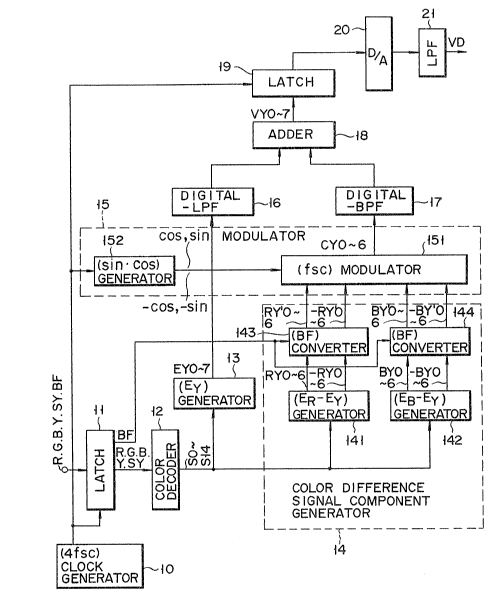
Referring to Fig. 1 illustrating a video encoder
circuit according to a first embodiment of the present
invention, latch 11 samples a digital signal including
red, green, blue, luminance and composite sync signals
R, G, B9 Y and SY output in synchronism with raster
scanning under the control of a display controller in a
lû digital signal source (not shown) such as a videotex or
teletext system. This digital signal also includes
burst flag signal BF representing a color burst super-
posing position. Among the signals sampled by latch 11,
signals R, G, B, Y and SY are converted into corre-
sponding color information signals S0 to 514 by colordecoder 12.
Luminance signal component generator 13 converts
luminance signals EY of colors represented by color
information signals Sû to 514 into binary data bits EYû
to EY7. Color difference signal generator 14 converts
color difference signals ~ER - EY and EB - EY) of red
and green into binary value data signals RYo 6~ -RYo 6
BYo 6 and -BYo 6. Generator 14 generates binary value
data signals RY'0_6, -RY 0-6' 0-6 0 6
corresponding to the amplitudes of color burst signals
during generation of burst flag signals BF. Modulator
15 performs balanced modulation of color subcarriers
~s~
-- 8 --
having phases shifted by 90 degrees, by usiny the two
color difference signals output from generator 14.
Modulator 15 then outputs carrier chrominance signal
component CYo_6-
Digital low-pass filter 16 performs an arithmetic
operation having the same characteristics as a normal
analog low-pass filter. This arithmetic operation is
performed for luminance signal component EYo 7 generated
by generator 1~, thereby limiting interference to the
lû carrier chrominance signal component. Digital band-pass
filter 17 performs the same operation as described
above. This operation is performed for component BYo 6
thereby preventing interference to the luminance signal
component. The luminance signal component from the
low-pass filter and the carrier chrominance signal from
the band-pass filter are added by adder 18 to proauce
digital video signal component VY0 7. This video signal
component is latched by latch 19 and converted into an
analog video signal by D/A converter 20 at a proper
timing. The high frequency component of -the analog
video signal is cut off by normal analog low-pass filter
21, thereby outputting (analog) video signal VD.
The operation of the circuit having the above
arrangement will be described below.
Digital signals R, G, B, Y, SY and BF, output from
a display controller (not shown), are latched and
sampled by latch 11 in response to clocks having
~5~
g
a frequency 4fsc (fsc is the color subcarrier
frequency). Signals R, G and B are color information
signals representing 8 different colors, and signal Y is
color information signal representing two luminance
levels. Color decoder 12 converts each color
information into one of color information signals SO to
514. The circuit arrangement and operation sta-te of
color decoder 12 are respectively shown in Figs. 2 and
3. Referring to Fig. 2, signals R, G and R are
selectively supplied to NAND gates 121-1 to 121-8
directly and through inverters 123-1 to 123-3 to
determine which one of colors (white, yellow, magenta,
red, cyan, green, blue and black) is represented by the
input signals. The decoded results are selectively
input to OR gates 122-1 to 122-14 directly and signal Y
is supplied thereto directly and through inverter 123-4
to determine whether each decoded result represents one
of the luminance levels (i.e., full luminance and half
luminance). The input signals are decoded such that one
of signals SO to 514 is set at level ~L~ for 15 colors,
i.e., 8 tcolors) x 2 (luminance levels) (~black~ has
only one luminance level), as shown in Fig. 3. If
signal SY is set at level ~ILt~ during the period of
composite sync signal, the NAND and OR gates convert all
signals SO to S14 into "H" level signals, thereby
simplifying subsequent signal processing.
In t he normal NTSC scheme, luminance signal EY and
- 10 -
two color difference signals ER - EY and EB - EY of each
of three primary color signals ER, EG and EB are repre-
sented by the following equations:
EY = 0.30ER + 0.59EG + û.11EB ............ (1)
ER - EY = 0.70ER - 0.59EG - 0.11EB ....... (2)
EB - EY = -0.30ER - 0.59EG + 0.89EB ...... (3)
In order to prevent overmodulation, the amplitudes of
signals ER - EY and EB - EY are limited to 1/1.14 and
1/2.03, respectively. Therefore, the relative values of
luminance signal EY and color difference signals (ER -
EY)/1.14 and (EB - EY)/2.03 are given as values in
Fig. 4. When the relative amplitude values of the color
bar signals for a monitor test-pattern are represented
by using the above values in association with the
timings o~ signals R, G, B, Y, SY and BY, they are as
shown in F1g. 5. In this embodiment, the ratio of full
luminance to half luminance is set to be 2 : 1.
However, the ratio may be obtained by using y-corrected
values.
To each color component detected by decoder 12,
that is, each of 15 color components, i.e., 8 colors x 2
luminance levels - 1 and a sync signal, luminance signal
component EY and two color difference signal components
(ER - EY)/1.14 and (EB - EY)/2.03 are generated as
binary value data9 as shown in Fig. 6. In this case,
component EY and components ~ER - EY)/1~14 and ~EB -
EY)/2.03 are timed with the sync signal. In this
~s~
embodiment, for simplifying subsequent digital
processing, each value shown in Fig. 5 is multiplied 100
times, and the value of level IILII of the sync signal is
set to be ~0~. It should be noted that a negative value
is a 2's complement number. Component EY is generated
by luminance signal component generator 13 whose
arrangement is shown in detail in Fig. 7. More
specifically, color information signals S0 to 514 from
color decoder 12 are decoded accordin~ to the relation-
ships defined in the column of EY in Fig. 6 and 8-bit
signals EYo 7 are generated. For example, signal EY7 is
set at logic ~ only if the input signals represent
white or yellow with the full luminance. Then, NAND
gate 13-7 gates signals S14 and S12. In the case of the
sync signal, all color information signals S0 to S14 are
set at level ~H~, so that signals EYo 7 are set at logic
.
Similarly, color information signals Sl to S12
(signals S0, S13 and S14 are set at logic l10~l an~ can be
omitted) are respectively decoded by (ER - EY) gen-
erator 141 and (EB - EY) generator 142 according to the
relationships given in the columns of ~ER - EY)/1.14 an~
(EB - EY)/2.03 in Fig. 6, and color difference signal
components (ER - EY)/1.14 and (E8 - EY)/2.03 are output
as signals RYo 6 and BYo 6' respectively. In order to
simplify subsequent processing3 inverted outputs -RYo 6
and ~Yo 6 are also output. (ER - EY) generator 141 for
_ 12 -
generating signals RYo 6 and -RYo 6 is shown in detail
in Fig. 8. ~EB - EY) generator 142 can be designed in
the same manner as in generator 141.
ln an NTSC video signal 9 color subcarrier having
phases shifted by 90 degrees, that is, cos2~fsct and
sin2~fsct, are balanced-modulated with two color
difference signal components (ER - EY)/1.14 and (EB -
EY)/2.03 to prepare carrier chrominance signal CY.
Video Signal = EY ~ CY ...(4)
CY = {(ER - EY)/1.14}cos2~fsct
+ {(EB EY)/2.03}sin2~fsct ...(5)
Components cos2~fsct and sin2~fsct represent waveforms
having phases shifted by ~0 degrees, as shown in
Figs. 9A and 9B, respectively. In order to perform
digitally balanced modulation, values of color differ-
ence signal components tER - EY)/1.14 and (EB - EY)/2.03
and the values obtained by multiplying the above values
with ~ are switched to each other with 4fsc. More
specifically, if a sampling point of components
cos2~fsct and sin2~fsct is defined as follows:
t = n/4fsc (for n = 0, 1, 2, 3,...) ...(6)
signal CY can be obtained by using tER - EY)/1.14, (EB -
EY)/2.03, -(ER - EY)/1.14, -(EB - EY)/2.03,.... There-
fore, signals RYo 6' -RYo_6 and BYo_6 a 0-6
(ER - EY) and (EB - EY) generators 141 and 142 are
switched by color subcarrier (fsc) modulator 151 in an
Yo-6' BY0-6' -RYo 6' -BYo 6' thereby
~ 13 -
completing balanced modulation. In this case, since
generators 141 and 142 generate signals -RYo 6 and
-BYo 6 the arrangement of modulator 15 can be simplified.
Since the color burst signal is superposed on the
video signal during the burst period, as shown in
Fig. 5, two color difference signal components (ER -
EY)/1.14 and (EB - EY)/2.03 must be converted to the
color burst components during -the burst period. This
conversion is performed by burst flag (BF) converters
143 and 144. As shown in Fig. 5, the relative amplitude
value of the color burst signal is 0.2 (20 in this
embodiment) and its phase is an opposite phase of -the
signal EB - EY, as shown in Fig. 10. As is best shown
in Fig. 11, BF converter 143 causes AND gates Al to A14
to convert signals RYo 6 and -RYo 6 into ~10ll during the
burst period, i.e., while signal BF is set at level 'ILI',
thereby generating signals RY'o 6 and -RY'o 6. As shown
in Fig. 12, BF converter 144 causes inverter Il, OR
gates 01 to 06 and AND gates A15 to A22 to convert
2û signals BYo_6 and -BYo_6 into ~-20(11011002)~ and
"20(00101002)", thereby generating signals BY'o 6 and
-BY'o 6 However, if signal BF is set at level ~H~
i.e., in a period excluding the burst period, components
RYo 6 and -RYo 6 are output without modifications.
output signals RY'0_6, -RY 0-6~ BY 0-6 and 0-6
from BF converters 143 and 144 are subjecte~ to balanced
modulation in modulator 15. Modulator 15 comprises
~5~
- 14 -
subcarrier (fsc) modulator 151 for modulating the
subcarrier (fsc) by switching between two color
difference signal components and the components obtained
by multiplying the above signal components with ~
and sine-cosine switching pulse (sin cos) generator 152
for generating switching pulses cos, sin, -cos and -sin
required for switching. Generator 152 comprises a
4-stage ring counter using 4fsc (Fig. 14A) as a clock
pulse frequency, as shown in Fig. 13. ~he ring counter
comprises D flip-flops FFl to FF4 and NOR gate Nl. In
order to simplify initialization, pulse SPl (Fig. 14F)
from NOR gate Nl is used as a set pulse in place of
pulse -sin (Fig. 14E). The two color difference signal
components are switched in fsc modulator 151 by
switching pulses cos, sin, -cos and -sin (Figs. 14B to
14E) generated by generator 152 in an order of RY'o 6'
BY 0-6~ -RY 0-6 and -BY'0_6. As a result, carrier
chrominance signal component CYO 6 is derived by
balanced-modulating the subcarrier.
In order to prevent mutual interference between the
luminance and carrier chrominance signal components of
the video signal, their high- and low-frequency
components must be eliminated. In this embodiment,
digital low pass filter (DIGITAL-LPF) 16 performs the
operation so as to cut off the high-frequency component
of signal component EYo 7 Digital band-pass filter
(DIGITAL-BPF) 17 performs the operation so as to cut off
~$5~
_ 15 -
the low-frequency component of component CY0 6.
Fig. 15 shows the circuit arrangement of DIGITAL-
LPF 16 which comprises two lat:ches, an adder, and a 1/2
attenuator.
Referring to Fig. 15 showing the circuit arrange-
ment of DIGITAL-LPF 16, if three continuous sampling
points are defined as Xn, Xn_l and Xn_2, P n
is given as follows:
Yn = (Xn ~ Xn 2)/2 for n = 0, 1, 2,...
... (7)
If the time series consists of sampled values of sine
wave Xn = ein~T (representation of complex number):
Yn = (1/2)(1 ~ e~i2~T)ejn~T --(8)
H(eiWT)ein~T . ,. (9)
for H(ei~T) = cos~T e j~T, ~ = 2~f, and
T = 1/(4fsc)
Transfer function H(ei ) gives filter frequency charac-
teristics, and the absolute value of H(ei~T) has the
amplitude characteristics having an attenuation point at
fsc on the axis of frequency, as shown in Fig. 16.
DIGITAL-LPF 16 has low-pass characteristics.
Fig. 17 shows a circuit arrangement of DIGITAL-BPF
17. In Fig. 179 the front stage comprises a latch cir-
cuit and an adder, and the rear stage comprises two
latches, an adder, and a 1/4 attenuator.
DIGITAL-BPF 17 comprises two filters connected in
series with each other and having transfer functions
~2~S~
- 16 -
Gl(ei~T) and G2(ei~T) as follows:
Gl(ei~l)T) = Cos2~"T.e-j2~T
G2(ei T) = sin~T.e(~/2 - ~T)j
therefore, total transfer function H(ej T) is given as
follows:
H(ei~T) = Gl(ei~T)~G2(ei~T)
and the amplitude characterist:ics have fsc as the center
frequency and Fsc/2 and 3fsc/2 are attenuation points.
In other words, DIGITAL-BPF 17 has band-pass character-
istics. DIGITAL-LPF 16 and DIGITAL-BPF 17 have differ-
ent delay times so that a latch (not shown) is provided
to match the delay times.
The luminance signal component and the carrier
chrominance signal component which are filtered by
DIGITAL-LPF 16 and DIGITAL-BPF 17 are added by adder 1
to produce video signal VY0 7 represented by equation
(4). Latch 19 latches this video signal in response to
clocks having a frequency of 4fsc. In other words,
latch 19 outputs a binary digital value corresponding to
the amplitude value of the desired video signal for a
period corresponding to 4fsc.
Digital value VY0 7 is converted into an analog
value by D/A converter 20, and the high-frequency
component thereof is cut oFf by normal analog low-pass
filter 21, thereby extracting analog video signal VD.
According to the first embodiment as described
above, when the digital chrominance signal output From
- 17 -
the display controller is encoded to the analog video
signal, most of the encoding operations are digitally
performed. ~nlike in conventional analog processing,
analog peripheral components such as resistors, capaci-
tors, inductors, or delay lines can be omitted. There-
fore, potential problems caused by degradation of
resistors or the like can be eliminated, and stable
electrical characteristics can be maintained Further-
more, since adjustment of the peripheral components need
not be performed, assembly can be simplified and hence
circuit reliability can be improved.
When the stage prior to the D/A converter is con-
stituted by a digital IC, a simple circuit arrangement
(i.e., the digital IC, the D/A converter and the
low-pass filter) can be used to generate the video
signal.
In the First embodiment, when the color subcarrier
waveforms having phases shifted by 90 degrees are
subjected to balanced modulation with two color
difference signal components to produce carrier
chrominance signal components, zero-crossing points of
the opposite subcarriers are selected as four modulation
points withln the fsc period, so that the color
difference signal components can be periodically
switched.
According to the first embodiment, digital filter-
ing is performed for the carrier chrominance signal
~5~
_ 18 -
components, so that the number of filters can be reduced
as compared with the case wherein two color difference
signal components are independently filtered.
A second embodiment of the present invention will
be described below. The same reference numerals as in
the second embodiment in Fig. 1 denote the same parts
in the second embodiment in Fig. 19, and a detailed
description thereof will be omit-ted. Carrier chromi-
nance signal CY as the color component at the time of
production of a video signal is obtained by balanced
modulation of cos2~fsct and sin2~fsct with two color
difference signal components (ER - EY and EB - EY).
Balanced modulation is performed such that the zero
point is selected as the modulation point, and binary
values corresponding to the amplitude values of the two
different color difference signals are switched at the
4fsc period. In this case, positive and negative values
are required as the amplitude values. The color
difference signal component generator for converting the
two different color difference signals into binary data
generates both the positive and negative values for each
color. For this reason, the size of generator 14 in the
~irst embodiment is large. In the second embodiment,
the circuit arrangement of the color difference signal
component generator is simplified.
A complementary color relationship of chrominance
signals is given, as shown in Fig. 20. For example,
5~
-- 19 --
color ~ has complementary color ~ . As is apparent
from Fig. 20, the color and its complementary color are
positive and negative with respect to the (ER - EY)-axis
and ~EB - EY)--axis, respectively. For example, if the
(ER - EY) component of a given color has a positive
amplitude value, its complementary color has a negative
amplitude value. If the (ER - EY) component of the
given color has a negative value, its complementary
color has a negative amplitude value. This is also true
for the (EB - EY) component.
Assume that color subcarrier components are
balanced-modulated with color difference signal
components (ER - EY) and (EB - EY). If a given color is
converted into its complementary color at a timing when
a negative value (i.e., a value obtained multiplying a
positive value by ~ ) of the color difference signal
component is required, the negative amplitude value of
the color difference signal component of the given color
can be obtained. According to this principle of opera-
tion, it is unnecessary for the color difference signalcomponent generator to generate both the positive and
negative values, thereby simplifying its circuit
arrangement.
Referring to Fig. 19 showing the second embodiment,
digital signals R, G, B, Y and the like are sampled by
latch 31 and converted into color information signals S0
to S14 corresponding to 15 colors, i.e., 8 (colors) x 2
~s~
- 20 -
(luminance levels) - 1 (since black has only one
illuminance level). This conversion is performed as
shown in Fig. 3. The amplitude values of the color
difference signal components (ER - EY)/1.14 and (EB -
EY)/2.03 are given as values :in Fig. 6. As is apparent
from Fig. 6, yellow and blue ~10 and -10 as decimal
amplitude values of the (ER - EY)/1.14 components there-
of; and ~44 and 44 as decimal amplitude values of the
(EB - EY)/2.03 components thereof), magenta and green
(52 and -52; and 29 and -29), red and cyan (61 and -61;
`and -15 and 15) are respectively complementary.
Complementary color converter 340 of color
difference signal component generator 34 serves as a
switching circuit for switching signals having the
complementary relationship described above at a timing
of the negative value (i.e., the value obtained by
multiplying the positive value by ~ ) when the sub-
carrier is modulated with the corresponding color dif-
ference signal. The above timing is l/?fsc or 3/4fsc in
Fig. 9, and pulse -cos or -sin in Fig. 14.
The detailed arrangement of complementary color
converter 340 is shown in Fig. 21. Referring to
Fig. 21, both pulses -cos and -sin are set at level
IIL~I at timings O and 1/4fsc in Fig. 9. An output
from NOR gate 340-1 is set at level ~H~, while an
output from inverter 340-2 is set at level ~L~.
Switches 340-3 comprising AND gates A31 to A54 and
- 21 -
OR gates 031 to 042 generate color information signals
Sl to S12 as complementary relationship information
signals Cl to C12, thereby obtaining the normal color
state.
Since either pulse -cos or -sin is set at level
~H~ at a timing of 1/2fsc or 3/4fsc, the output from
NOR gate 340-1 is set at level IIL'I and an output from
inverter 340-2 is set at level ~H~. The outputs from
switches 340-3 are signals Cl to C12, representing the
complementary relationship states of signals Sl to S12.
For example, signal S12 is set at level IIL'I and all
signals Sl to Sll are set at level ~H~ in the case of
yellow ~ith a full luminance. However, signal C2 of
level t~L~~ and signals Cl and C3 to C12 of level ~H~
appear at switches 340-3. This indicates a color state
of blue with a full luminance as the complementary color
of yellow with a full luminance.
Complementary color relationship information
signals Cl to C12 output from complementary color
converter 340 are decoded, and ~ER - EY) generator 341
and (EB - EY) generator 342 generate color difference
signal components (ER - EY)/1.14 and ~EB - EY~/2.03 as
7-bit signals RYo 6 and BYo 6' respectively. As best
shown in Fig. 22, generator 34~ may be designed to
generate only one of the positive and negative amplitude
values of the color difference signal components and can
be realized by a simple arrangement.
- 22 -
In order to perform balanced modulation of color
subcarrier components with signals RYo 6 and BYU 6' the
sampling points represented by equation (6) are selected
to sequentially switch signals RYU 6' BYo 6' RYo 6'
5 BYU 6~ in the order named. Since the color burst
component is output during the burst period, BF gen-
erator 343 always outputs signals Bû 6~1~-20~) and
-Bû 6t"20") representing the (EB - EY~-axis components
of the color burst. In other words, during the burst
lû period, signals ~ûll, Bû_6, l~ûll~ -Bo_6~ are
sequentially switched and output in place of signals
RYo 6 and BYo_6-
Modulator 35, comprising fsc modulator 351 andsin-cos generator 352, performs the above-mentioned
switching operation, and the subcarrier components are
blanced-modulated to generate carrier chrominance signal
component CYo_6-
Luminance signal component EYo 7 and carrier
chrominance signal component CY0 6 are filtered by
DIGITAL-LPF 36 and DIGITAL-BPF 37, respectively, and
added by adder 38, thereby obtaining digital video
signal VY0 7. Signal VY0 7 is processed by latch 39,
D/A converter 40, and LPF 41, and is output as analog
video signal VD.
According to the second embodiment as described
above, comp:Lementary color converter 340 is arranged to
convert a sl;ate of a given color into a state of i-ts
~%~
- 23 -
complementary color at a proper timing, so that the
arrangements of (ER - EY) and (EB - EY) generators 341
and 342 for generating the binary amplitude values of
the color difference signal components can be simpli~
fied. For example, the hardware of generators ~41 and
342 is reduced to i/2 that of generators 141 and 142 in
Fig. 1.
Since (fsc) modulator 351 switches only signals
RYo 6 and BYo 6' the circuit arrangement can be
advantageously made compact as compared with that of
(fsc) modulator 151 in Fig. 1.
The present invention is not limited to the R, G
and B signals as three primary signals and the color
difference signals ER - EY and EB - EY. So-called
chrominance signals EI and EQ, i.e.~ EI = 0.736(ER - EY)
- 0.268(EB - EY) and EQ = 0.478(ER - EY) + 0.41~EB -
EY), and color difference signal components correspond-
ing to these signals may be used. The number of colors
are not limited to 8 (colors) x 2 (luminance levels) -
1. The luminance and color difference signal componentsmay be decoded by using a larger number of bits, thereby
expressing a larger number of colors.
According to the present invent.ion, since an analog
video signal can be produced from a digital chrominance
by digital processing 9 circuit adjustment need not
be performed. Degradation of circuit characteristics
can be eliminated to further improve circuit reliability.