Note: Descriptions are shown in the official language in which they were submitted.
'~ `` 671.1
LIQUI~ CRYSTAL DISPLAYS OPERATED BY
AMORPHOUS SILICON ALLOY DIODES
The present invention relates generally to
displays and more particularly to displays which
are driven by diodes formed from deposited semi-
conductor materials.
There are many applications wherein liquid
crystal displays are utilized to advantage~ For
example, liquid crystal displays find use in digi-
tal watches, digital clocks, calculators, pocket-
si~ed tele~ n receivers, and various forms of
portable games, to name just a few~
Liqùid crystal displays generally include a
plurality of pixels (picture elements) arranged in
rot~s and columns~ Each pixel includes a pair of
electrodes~ As is well known, when a voltage is
applied across the electrodes, the optical proper-
ties of the liquid crystal material can be changed
to provide a light or dark display depending upon
the type of liquid crystal material ùsed and the
desired mode of operation of the display.
To obtain a usable display, the voltage po-
tential across the electrodes of each pixel must
be selectively applied. In the prior art, the
selective appllcation of these voltage potentials
has been accomplished through the use of thin film
transistors. While thin film transistors are gen-
erally successful in these applications, they can
only be used for small area liquid crystal dis-
plays. Conventional thin film transistors also
exhibit relatively high power dissipation and low
frequency operation. This limits the number of
~ els whicil c~n be driven in a liqui~ cr~stal
.isplay which in turll l;mi~s the liquid crystal
display areas.
~nother problem in using thin film transis-
5 tors in liquid crystal disp]ays is yield. Vir-
tually one-hundred percent of all of the thin film
transistors must be operational to obtain a usable
display . Such yields are difficult to achieve
o~er sr~lall display areas and virtually impossible
to achieve for large area displays because the
making of thin fil~ transistors requires numero~s
process steps, man~ of which require extremel~ ac-
cur~te photolithography. Accurate or precise
photolithography is required to control important
physical device dimensions, principal among them
being the source ~o drain spacing which deter-
~ines, in conventional planar thin film transis-
tors, the length of the current conduction channel
between the source and drain. The channel length
drama~ically effects both the device current and
operating frequency limit. ~s a result., the high
yields required cannot be readily achieved ~or
lar~e display areas with conventional photolitho-
~raphy techniques.
The present invention overcomes such defi-
ciencies exhibited by thin film transistors by
using diodes to drive the display pixels.` Fur-
thermo-re, the diodes can be formed without the
need of precise photolithography and in fewer pro-
cess steps than that required to form thin film
tr~nsistors.
--2--
~6~
The u~e of diodes to drive ~isplays has been
~reviously proposed. However, previously proposed
diode driven displays were limited to discrete
diod~ devices which of course are not appropriate
for large area displays employing potentially
thousands of pixels. Such displays would be nec-
essarily and undul~ complicated both physically to
imple~ent the indivi~ual pixels and electrically
to a~dress the individual pixels.
The present invention overcomes these prob-
lems hy for~ing the diodes integrally with the
display structure~ The diodes can be forme~ from
deposite~ semiconductor materials by processes not
incompatible with the other display processes.
We have found that the above disadvantages
may be overcome by employing the present invention
which provides a display incorporating a light in-
fluencing material and a subassembly for use in
such a display. The subassembly includes a sub-
strate, a pixel electrode of a selected shape
Lormed on the su~strate, a first address line
~ormed on the substrate, a second address line in-
sulated from the first address line and carried by
the substrate, a first isolation means formed on a
region of the first address line and coupled be-
tween the first address line and the pixel elec-
trode and a second isolation means formed on a
region o the pixel electrode and coupled between
the pixel electrode and the second address line.
Each isolation means can include a single diode or
alternately a plurality of vertically arrayed
series coupled diodes.
The present inventi~on also provides,
in a liquid crystal display, of the type having a-t least
one pixel element including a pair of electrodes and
liquid crystal display materi.al disposed between the
electrodes, -the improvement comprising the a-t least one
pixel element including at least a paIr of diodes ormed
~rom deposited semiconduc-tor material.
- 3a -
we have also found that ~he present invention
provi~es a liquid crystal display inc~uding at
least one pixel element wherein the pixel element
is formed on an insulative substrate and includes
S at least two address leads, a pair of series con~
nected diodes coupled between the address leads, a
first conductive electrode coupled between the
diodes, a second electrode spaced from the first
electrode, and liquid crystal display material
lQ disposed between the electrodes. The diodes are
formed from a deposited semiconductor material~
The deposited semiconductor material is preferably
an amorphous semiconductor alloy including sili~
con. ~he diodes preferably include a first doped
semiconductor region, an intrinsic semi~onductor
re~ion overlying the first doped region, and a
second doped semiconductor region o~posite in con~
duct vity with respect to the first doped region
overlying the intrinsic region.
In addition, we have ound that the present
invention further provides a liquid crystal dis-
play including at least one pixel element, com-
prising first and second pairs of diodes, each
diode pair being coupled in series relation, a
first pair of address leads coupled to respective
ends of one of the series coupIed diodes, a second
pair o~ address leads coupled to respective ends
of the other of the series coupled diodes, a first
electrode coupled to the junction of one of the
pair of diodes, a second electrode coupled to the
Junction of the other pair of diodes, and liquid
crystal display material disposed between the
electrodes.
- 3~ -
~L2~;58~
~ ;e ilave fo~nd ~ha~ the present invention also
~rovides a ~et`~od o mal<ing ~ liquid cryst~ lis--
play including at l~ast one pix~l element. The
l~etho~ includes the steps o providing an insula-
S ~ive su~strate, forming an ;nterconnect lead andan ~ddress lead on the substrate in spaced apart
reiation, rorming a diode on each of the leads,
~or~in~ a layer of insulative material between the
diodes, forming an openin3 in the insulative layer
1~ communicating t~ith the interconnect lead, forming
a conductive electrode over the insulative layer
in cont~ct with the diode formed on the address
leac~ and in contact with the interconnect lead
through the opening, forming another address lea~
lS contacting the diode formed on the interconnect
lead, applying liquid crystal display material
over at least the conductive electrode, and form-
ing a second conductive electrode over the liquid
crystal display material.
We have found that the present invention
still ~urther pro~7ides a ~ethcd of mal~ing a liquid
crystal ~isplay includiny at least one pixel ele-
ment including the steps of providing an insula-
tive substrate, forming an interconnect lead and
an address lead on the substrate in spaced apart
relation, forming a diode on each of the leads,
and orming a layer of insulative ~aterial between
the diodes~ The method further includes forming
an opening in the insulative la~er communicating
~ith the interconnect lead, forming a conductive
electrode over the insulative layer in contact
with the diode for~ed on the address lead and in
~ 3c -
~26~;~36~L
contact with tlle in~ercorlllect lead throuyh the
openill~" and forming another address lead contact-
ing the diode forMed on thQ interconnect lead~
The fore~oing steps are re?eated to form
first ~nd second subassemblies~ Therea~ter, liq-
uid cr~-stal display material is applied over at
least ~he electrode of one of the subasse~blies
and the electrode of the other subassembly is
aligned with the electrode of the one subasse.~bly
~ith the liquid crystal display material therebe-
t~een.
- 3d -
~z~
~ e h~e also found that the present invelltion
provides for a display incorporating a light in-
fluenciny m~terial havinc~ an insulated substrate,
a first pi~el electrode ~ormed on the substrate, a
first address line formed on the substrate, a
first isolation device formed on the first address
line, a second isolation device formed on the
pi~el electrode, a second address line insulated
from the first address line and in electrical con-
1~ nection with the second isolation device, a con-
ductive material coupling the first isolation de-
vice to the first pixel electrode, a second pixel
electrode spaced apart from and substantially par-
allel to the first pixel electrode and the light
influencing material disposed between at least the
~ixel electrodes. Each isolation device can in-
clude a single diode or alternately a plurality o
vertically arrayed series coupled diodes. The
isolation devices ~ay be ~ormed as a diode ring.
~0 A subassembly ror a ~isplay pixel is 21so
provid^d by ~hQ present invention. The subassem-
bly includes a substrate, a pixel electrode formed
thereon, an address line formed adjacent the pixel
electrode, and first and second isolation struc-
?5 tures formed on the address line and the pixel
electrode respectively. A deposited layer of
metal connects the first isolation structure to
the pixel electrode. A second layer of metal con-
nects the second isolation structure to a second
address line.
--4--
The isolation devices of the subasse~bly and
the display of ~he present inven~ion can be diodes
formed fror,l an amor~hous silicon alloy. The alloy
may contaiil hydrogen and/or fluorine.
In addition~ we have found that the invention
provides for a method of making a subassembly for
a dis~lay having at least one pixel and a pair of
isolation devices. The method includes the steps
of providing a substrate, depositing a conductive
layer over the substrate, depositing a first metal
layer over ~he conducting ~aterial, depositing a
first doped semiconductor layer over the first
metal layer, depositing a substantially intrinsic
semiconductor layer over the first doped layer,
depo~iting a second doped se~iconductor layer over
the intrinsic layer; the second doped layer being
opposite in conductivity with respect to the first
- doped layer, and deposl'ing a second metal layer
over the second do~ed semiconductor iaye~. The
method further provides Lor removin~ ~er-iols of
the second metal layer so as to leave discrete
regions thereof to define the locations of isola-
tion devices, removing portions of the semicon-
ductor layers while using the discrete metal
reyions as masks to form the isolation devices,
removing portions of the first metal layer to form
an address line with one of the isolation devices
formed thereon, removing portions o~ the conduc-
tive ~aterial to form a first pixel electrode with
the other isolation device positioned thereon,
coupling the first isolation device to the pixel
electrode, forming a second address line insulated
from the first address line and coupled to the
--5--
~2 E;~
ot~ler iso]~tion device. r~,e method also provides
for ferming ~ second pi~el electrode spaced a~art
fro-n and su~s~antially par~].lel to the first ~ixel
electrode ~nd applying light inLluencing material
betwee~ the pixel electrodes.
The me~hod also provides for carrying out the
steps of depositi.ng tlle layers of semiconductor
material in a partial vacuum such that the partial
vacuum is continuously maintained during the depo-
1~ sition of the layers of semiconductor material.The method al~o provides for forming the pixel
electrodes of a transparent conducting material
such as indium tin oxide.
The method also provides for forming a plu-
rality of vertically arrayed isolation devices outof a plurality of deposited amorphous semicon-
ductor alloy layers. The plurality of vertically
overlying p-i-n amorphous silicon alloy layers can
be etched so as to form first and second vertical-
ly arrayed, series coupled, stacks of isolation
diodes. ~ series coupled stack of amorphous sili-
con alloy isolation devices will support a greater
reverse bias voltage than will a single isolation
device.
The method also provides for forming a diode
ring coupled between an address line and a pixel
electrode out of a plurality of deposited amor-
phous semiconductor alloy layersO The diode ring
can include parallel coupled isolation devices
each of which can be formed frorn one or more
series coupled amorphous silicon alloy diodes.
The isolation devices are parallel coupled with
reverse polarity to form the ring. The method
provides for forming the first and second isola-
tion devices on the address line and on a region
of the pixel electrode respectively, offset with
respect to one another. The method also provides
for depositing first and second metal layers to
couple the first isolation device formed on the
address line, to the pixel electrode and to couple
the second isolation device, formed on the pixel
electrode, to the address line.
We have also found that the invention pro-
vides for a subassembly for a display having an
insulative substrate, conducting electrode formed
thereon and first and second nonintersecting de-
posited address lines coupled to the electrode~
The address lines are formed essentially parallel
to one another,
The light influencing material can be a
liquid crystal display material including conven-
tional nematic liquid crystal display materials.
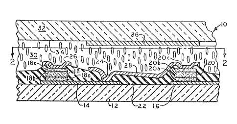
Fiyure 1 is a cross-sectional side view of a
liquid crystal display pixel;
Figure 2 is a top plan view as seen along
lines 2-2 of Figure l;
Figure 3 is a schematic circuit diagram il-
lustrating the equivalent circuit of the liguid
crystal display pixel of Figure l;
Figure 4 is a cross-sectional side view of
another liquid crystal display pixel;
Figure 5 is a schematic circuit diagram il-
lustrating the equivalent circuit of the liquidcrystal display pixel of Figure 4;
Figure 6 is a cross-sectional side view of
another liquid crystal display pixel;
~L~;6~
~ igure 7 is a scilematic circuit dia~ram il-
lustra~ing the equivalell~ circuit o~ the liquid
crystal display pixel of Figure 6;
Fiyul-e 8 is a cross-sectional side view of a
liquid cr~stal display pixel embodying the present
inven_ion;
~ igures 9-15 are cross-sectiona]. side views
illustrating the method of making the liquid crys-
tal display pixel of Figure 8 at various stages
thereo~ in accordance with the present invention;
Figure 16 is a cross-sectional side view of
a~other liquid crystal display pixel embodying the
~resent invention;
Figure 17 is a cross-sectional side view il-
lustrating in part another method in accordancewith the present invention;
Figure 18 is a schematic circuit diagram of
the liquid crystal display pixel of Figure 16;
Figure 13 is a schematic circuit diagram il-
lustrating the equivalent circuit of another em-
bodi~er,t of a liquid crys~al display ~ixel em~ody--
ing the present invention;
Figure 20 is a cross-sectional side view il-
lust.rating one step in the method of making the
liquid crystal display pixel illustrated schemati-
cally in Figure 19;
Figure 21 is a fragmentary top planar view of
the liquid crystal display pixel illustrated in -
Figure 19;
3~ ~igure 22 is a cross-sectional side view of
a~other step in the processing of the liquid crys-
tal displa~ pixel of Fiyures 19 and 21;
--8--
5~
Figure 23 is a cross-sectional side view of
~he liquid crystal display pixel of ~lgures 19 and
21.
Referrin3 I-OW to Figures 1 and 2t they illus-
trate a display pixel 10. Altho~gh just one dis-
~lay ~ixel 10 is illustrated, it can be appreciat-
ed that many Suc]l pixels can be formed in, for
e~ample, a row and column arrangement to provide a
complete liquid crystal display. It will be un-
1~ derstood that none of the figures are drawn toscale. It will also be understood the proportion-
ate size of some of the electronic structures may
be enlarged for the purpose of providing an enabl-
ing disclosure.
The display pixel 10 includes an insulative
substrate 12 which can be formed from glass, for
exa~ple. Formed on the glass substrate 12 is an
interconnect bus or lead 14 and a first address
lead 160 The interconnect lead 14 and first ad-
~0 dress lead 16 can be formed from a conductive
material such as metal, for e~ample, aluminum,
molybdenum, or a molybdenum tantalum alloy. Other
suitable metals are chromiu~, tantalum tungsten,
` palladium and platinum. The interconnect lead 14
~S and first address lead 16 are formed by, for exam-
ple, S-gun magnetron sputtering the metal over the
encire surface area of the glass substrate 12 and
then removing selected portions of the deposited
metal by utilizing a mask and photolithography
techniques of the type well known in the art.
The display pixel l0 further includes a pair
of diodes 18 and 20 formed on the interconnect
lead 14 and first address lead 16, respectively.
The d o~les 18 and 20 are pre~erably formed ~ro~ a
deposited semiconductor m~terialO The deposited
sellliconductor m~teri(~l is preferably an amor~holls
semiconductor alloy including silicon. The amor-
phous silicon alloy can also include hydrogenand/or flu3rine and can be deposited by plasma
assis~ed chemical vapor deposition i.e. glow dis-
cllarge as disclosed, ~or example, in United States
Patellt No. 4, 226,898 which issued on October 7,
ln 198~ in the names of Stanford R. Ovshinsky and
Arun ~ladan for ~morphous Serniconductors Equivalent
To Crystalline Semiconductors Produced By A Glow
~ischarge Process. The diodes 18 and 20 prefer
ably have a p-i-n configuration formed by a first
i5 doped region 18a and 20a, which can be p-type, an
intrinsic region 18b and 20b overlying the first
~oped regions 18a and 20a respectively, and a
second doped region 18c and 20c, which can be
n-type, overlying the intrinsic regions 18b and
20b respectively.
The diodes 18 and 20 can be formed more spe-
cifically by depositing the previously mentioned
amorphous silicon alloy regions over the entire
surface area of the substrate 12 and interconnect
lead 14 and first address lead 16 and thereafter
selectively etching portions of the amorphous sil-
icon alloy regions by utilizing a suitable mask
and conventional photolithography techniques. Tne
mask utilized during the etching process prefer-
ably defines a diode configuration wherein eachdiode is about 20 to 50 microns on a side. Repre-
sentative thicknesses for the arnorphous sil iCOIl
alloy regions can be, for example, 300 Angstroms
--10--
t~ 1,?00 An~strorns and pre~erably 500 Angstrolns
ior th-~ p-type regions, 1,000 Angstroms to 10,000
~ngstr~ms a~d preerably 3,000 Angstro~s for the
intrinsic regions, and 100 Angstroms to 500 Ang-
S stroms and preferably 20n Angstroms for the n-type
regions.
Formed over the interconnect lead 14, the
substrate 12, and the first address lead 16, and
in between the diodes 18 and 20 is a layer of in-
la sulat~ng material 22. The layer of insulatingmaterial 22 can be formed from any deposited in-
sulator such as silicon oxide (SiXOy) or silicon
nitride ~SiXNy), or a polyimide, for example. The
insulating layer 22 defines an opening 24 which
communicates with the interconnect lead 14. The
configuration of the insula_ing layer 22 c~n be
obtained by roller, ex~rusion, or s?in coatin3 the
polyi~ide, for exa~ple~ o~er the enti~e sur a^e
area, spin coa~in~ _ layer of photoresls~ over the
20 polyimide layer, and then exposing ~nd Qeveïoping
out ~oth of the photoresist and ~he polyi~ide ~s--
ing a further mask. This step forms the opening
24 communicating with the interconnect lead 14 and
uncovers upper surface portions of the n-type
amorphous silicon alloy regions 18c and 20c of
diodes 18 and 20.
The display pixel 10 further includes a
second address lead 26 in electrical contact with
the n-type region 18c of diode 18 and a first
electrode 28 which is an electrical connection
with the interconnect lead 14 through the opening
24 and the n-type region 20c of diode 20. The
first electrode 28 and the second address l~ad 26
ii8~i~
can be formed Erom any of the metals previously
re~erred to with respect to the interconnect lead
14 and the first address lead 16 by sputtering the
metal over the entire surface area of the polyi-
mide 22, the exposed surface portions of thediodes 18 and 20, and the opening 24. The second
address lead 26 and the first electrode 28 can
then be configured by utilizing a suitable mask
and conventional photolithography techniques.
The address leads 16, 26 are formed out of
deposited metal essentially parallel to one
another, as can be seen from Figure 2, and both
are coupled to the first electrode 28. The diodes
18, 20 form an isolator coupled to the firs~ elec-
trode 28. The isolator formed of the diodes 18,
2n has first and second inputs to which the ad-
dress lines 26, 16 respectively are coupled.
Forming the address leads 16, 26 so that they
do not cross is advantageous from a manufacturing
perspective. When address lines cross a layer of
insulator, such as silicon dioxide, must be posi-
tioned therebetween so as to isolate one address
line from the other. Such insulator pads at times
are formed with pinhole defects that result in the
two address lines coming into electrical contact
with one another. Elimination of these crossovers
reduces the possibi~ity of such defects, Addi-
tionally, elimination of these crossovers simpli-
fies the overall structure of the display.
Speed of addressing is also enhanced by elim-
ination of crossovers. Each crossover forms a
capacitor with the insulator forming a dielectric
between the adjacent regions of the respective ad-
-12-
dress lines. Since a yiven array could have a
plurality of crossover points, a substantial re-
duction in capacitance can result.
It must be appreciated that the structures
illustrated in Figures 1 and 2 are not drawn to
scale and that the first electrode 28 defines the
display area of the display pixel 10. The first
electrode 28 can be configured in a square con-
figuration as illustrated in Figure 2 and can be,
for example, 300 microns to 2,000 microns on a
side depending on the overall size of the finished
display matrix and the desired aspect ratio.
With the first electrode 28 contacting the
interconnect lead 14 through the opening 24, the
diodes 18 and 20 are connected together in series
relation. As can also be note~ in Figure 1, the
address leads 16 and 26 are only in electrical
connection with the first electrode 28 through the
diodes 18 and 20.
Overlying the resulting structure described
above, is a layer of light influencing material
30. By the term "light influencing material" is
meant any material which emits light or can be
used to selectively vary the intensity, phase, or
polarization of light either being reflected from
or transmitted through the material. Liquid crys-
tal material is only one such material having
these characteristics. The light influencing
material 30 can be of any conventional variety, as
for example, nematic liquid crystal display mate-
rial.
-13-
The display pixel 1~ is completed ~ith a top
trans~arent insulative plate 32 forrned from, for
e.Yample/ gl~ss. On the inner surface 34 of the
insulative plate 32 is formed a layer of transpar~
ent conductive material 36 which can be, for exam-
ple, indium tin oxide. The indium tin oxide layer
36 forms a second electrode of the display pixel
10 which is in contact with the liquid crystal
material 30. It is conEigured to have the same
dimension as tlle first electrode 28 and is aligned
therewithO The top insulative plate 32 is polar-
ized in a manner ~ell known in the art consistent
with tlle type of liquid crystal display material
(light influence material 30) utilized in the dis-
play ~ixel 10. An alignmen~ coating of a conven-
tional type can be applied over the first elec-
trode 28 for the pur~ose of aligning molecules in
the liquid crystal display material 30.
Reerring now to Figure 3, it illustrates the
~0 equivalent circuit diagram of the pixel 10 of
Figure 1. As can be noted from Figure 3, the
pixel 10 includes the address leads 16 and 26, a
pair of series connected diodes 18 and 20 coupled
between the address leads 16 and 26, and the first
conductive electrode 28 coupled between the
diodes. The pixel 10 further includes the second
electrode 36 spaced from the first electrode 28.
In between the electrodes 28 and 36 is the liquid
display material 30.
As previously explained, the useful lie of a
nematic liquid crystal display can be extended if
the polarity of the applied voltage potential is
reversed during alternate frames. This can be ac-
-14-
~2Çi~36~
com~lished ~itl~ the pixel lO of Figure 1 by im-
~;essing a positive potential onto first address
lead 16 and a negative potential onto ~he second
electrode 36 during one frame to forward bias
S diode 20 and by impressing a negative potential
onto the second ad~ress lead 26 and a positive
potential on the second electrode 36 during the
next frame. Repeating this sequence causes the
potential applied to the liquid crys~al display
~a~erial to be reversed during alternate frames.
~ eferring no~ to Figure 4, it illustrates
another liquid crystal display pixel 40 structured
in accordance with another embodiment of the pres-
ent invention. The pixel 40, as will be appreci-
ated hereinafter, includes two pairs of diodes andis formed by first and second subassemblies 42 and
~4 respectively.
Each of the subasse~i~lles 42 and 4 are ~u~-
stantially identiccl to the portion of the l quid
crystal display pixel 10 of Figure 1 ~en~2~:r. the
liquid ~rystal display ma.erial 30. Essentially,
the second subassembly 44 is the mirror image of
the first subassembly 42.
I.ike the pixel 10 of Figure 1, the first sub~
assembly 42 includes an insulative substrate 52
which can be formed from, for example, glass. The
first subassembly 42 further includes an inter-
connect lead S4, a first address lead 56, and a
first pair of diodes 58 and 60 which can be sub-
stantially identical to the p-i-n diodes 18 and 20
of pixel 10. ~etween the diodes 58 and 60 and de-
fining an opening 64 communicating with the inter-
connect lead S4 is a layer of insulative material
~z~
62 which can be a polyi~ide, for exarnple. The
first subassembly 42 is completed with a second
address lead 66 and a first electrode 68. The
first subassembly 42 can be fabricated by the same
method as described with respec~ to the pixel 10
of Figure 1 and therefore need not be reiterated
herein.
The procedure by which the first subassembly
42 is fabricated can be repeated to provide the
second subassembly 44. To that end, as can be
noted ~rom the Figure, the second subassembly 44
also includes an insulative substrate 72, an in-
terconnect lead 74, a first address lead 76, a
second pair of diodes 78 and 80, an insulating
layer 82 defining an opening 84 communicating with
interconnect lead 74, a second address lead 86,
and a second electrode 88. If the liquid crystal
display material 70 between the subassemblies 42
and 44 is to be viewed through the æecond sub-
assembly 44, then the second electrode 88 shouldbe formed from a transparent conductive material,
such as, for example, indium tin oxide and the in-
sulative substrate 72 should be formed from a
transparent material such as glass which is polar-
ized in a manner consistent with the liquid crys-
tal display material 70 utilized between the sub-
assemblies. It will be understood that conven-
tional molecular alignment coatings and polarizers
will be incorporated into the subassemblies, such
as 42 and 44, disclosed herein as would be known
to those of skill in the art.
AS was the case with the a~dress lines 16, 26
(referred to in Figure 1) the address lines 56, 66
and 76, 86 (in Figure 4) are formed with no cross-
overs~ Each pair of address lines 56, 66 and 76,
86 is coupled to a respective electrode 68 or 88.
The structure of Figure 4 has the same advantages
as does the previously discussed structure of
Figures 1, 2 with respect to the noncrossing ad-
drèss lines.
Referring now to Figure 5, it illustrates the
equivalent circuit diagram of the pixel 40 of
Figure 4. As can be noted from the diagram, the
pixel 40 includes a first pair of diodes 58 and 60
and a second pair of diodes 78 and 80. Each pair
of diodes is coupled in series relation. The
pixel 40 further includes a first pair of address
leads 56 and 66 coupled to the respective ends of
the series coupled diodes 58 and 60 and a second
pair of address leads 76 and 86 coupled to respec-
tive ends of the other pair of series coupleddiodes 78 and 80. The first electrode 68 is
coupled to the junction of the diode6 58 and 60
and th~ second electrode 88 is coupled to the
junction of the diodes 78 and 80. Lastly, liquid
~5 crystal disp]ay material 70 is disposed between
the electrodes 68 and 88.
Like the pixel 10 of Figure 1, the potential
applied to the liquid crystal material 70 can be
reversed during alternate frames. During one
~rame, a positive potential can be applied to ad-
dress lead 76 and a negative potential to address
lead 66. During alternate frames, a positive
potential can be applied to address lead 56, and a
-17-
~;;
negative potential to address lead 86. In this
manner, the potential applied to the liquid crys-
tal material 70 can be reversed during alternate
frames.
Reerring now to Figure 6, it illustrates a
further liquid crystal display pixel 90 The
pixel 90 is formed on an insulative substrate 92,
such as glass, for example. ~ormed on the glass
substrate 92 is a first address lead 94. The
first address lead 94 can be formed from a conduc-
tive metal as in the previous embodiments and can
be, for example, aluminum, molybdenum, or a molyb-
denum tantalum alloy. Other suitable metals are
chromium, tantalum tungsten, palladium, and plati-
num. The first address lead 94 can be formed by,for example, S-gun magnetron sputtering the metal
over the entire surface area of the glass sub-
strate 92 and then removing seleted portions of
the deposited metal ~y using a mask and photo-
lithography techniques of the type well known inthe art,
The pixel 90 further includes insulating
layer 96 and insulating portions 104. The in-
sulating layer 96 and portions 104 can be formed
from any deposited insulator such as silicon oxide
or silicon nitride. During the photolithoyraphy
step in forming the insulating portions 104, open-
ings 106, 108, and 110 can be formed therein to
expose surface portions of the n-type reyions of
the diodes 100 and 102 and a surface portion of
the first interconnect lead 98.
-18-
, --
~2~1~
The pixel 90 further includes a bottom elec-
trode 112 and a second interconnect lead 114~ The
bottom electrode 112 and second interconnect lead
114 can be formed from any of the metals previous-
S ly referred to and by S-gun magnetron sputtering
the metal over the entire surface area and there-
after removing selected portions thereof by con-
ventional photolithography techniques. As will be
noted from Figure 6, the second interconnect lead
114 contacts the address lead 94 and the n-type
region lOOc of diode 100 through the opening 106
o the insulating portions 104. The bottom elec-
trode 112 contacts the first interconnect lead 98
through the opening 108 and the n-type region 102c
of diode 102 through the opening 110. As a re~
sult, the anode of diode 102 is coupled to the
cathode of diode 100 and the anode of diode 100 is
coupled to the cathode of diode 102. Also, the
joint connection between the anode of diode 100
and the cathode of diode 102 is coupled to the
irst or bottom electrode 112.
The pixel 90 further includes an insulative
transparent plate 116 which has a transparent con-
ductive material 118 deposited on its inner sur-
face to form the second electrode of the pixel
90. The transparent conductor 118 is con~igured
to have the same dimensions as the effective di-
mensions of the bottom electrode 112 and is align-
ed therewith. Disposed between at least the elec-
trodes 112 and 118, and in contact therewith, is
liquid crystal display material 120, which can be,
for example, nematic liquid crystal material of
the type well known in the art. The top transpar-
--19--
6~
en~ plate l16 as well as the lo~er plate 92 call
`e, as in the previous embodiments, polarized in a
~ann~- consis~ent with the type of liquid crystal
display material 120 utili~ec~ in the display.
~eferring now to Figure 7, it illustrates the
e~uivalent schematic circuit diagram of the liquid
crystal display pixel 90 of Figure 6. As can be
noted in Fiyure 7, the pixel includes the pair o-f
diodes 100 and 102 with the cathode of diode 100
and the anode of diode 102 coupled together and
also coupled to the first address lead 94. The
anode of diode 100 and the cathode of diode 102
are also coupled together and to the first elec-
trode 112~ The second electrode 118 is coupled to
a second address lead 122 (not shown in ~igure 6)
and the liquid crystal display material 120 is
disposed between and in electrical contact with at
least the electrodes 112 and 118.
Like the pixels of the previous embodiments,
the potential applied to the liquid crystal mate-
rial 120 can be reversed during alternate frames.
During one frame, a positive potential can be ap-
plied to first address lead 94 and a negative
potential to second address lead 122. During
alternate frames, a positive potential can be
applied to second address lead 122, and a ne~ative
potential to first address lead 94. In this man-
ner, the potential applied to the liquid crystal
material 120 can be reversed during alternate
frames.
Figure 8 illustrates an embodiment of the
present invention. A single pixel 140 of a dis-
play which incorporates a subassembly 142 is il-
-20-
lustrated in Figure 8. Spaced apart Erom the sub-
assembly 142 is an insulating transparent sub-
strate 144 which can be Eormed of glass and upon
which is formed a pixel electrode 146. The pixel
electrode 146 may be formed of transparent indium
tin oxide. Between the ~ubstrate 144, ~he pixel
electrode 146 and the subassembly 142 is a region
148 which is filled with a light influencing mate-
rial~ For example, nematic liquid crystal mate-
rial of a conventional type may be used.
The subassembly 142 includes an insulatingsubstrate 1 0, such as glass, upon which is formed
a pixel electrode 152. The suhassembly 142 also
includes a first address line 154 formed on the
insulating substrate 150 and a second address line
156 insulated from the first address line 154 and
carried by the insulating substrate 150. An iso-
lation device 158, preferably a p-i-n diode, is
formed on a region of the first address line 154.
A silicon dioxide layer 160, or equivalent insula-
tor as previously disclosed, surrounds the diode
158 and covers the first address line 154 except
in a regiQn or via 162~ A metal deposit 164 ex-
tends throuyh the via 162 and is in contact with
the isolation device 158. The metal deposit 164
couples the isolation device 158 to the pixel
electrode 152.
A second isolation device 166, also prefer-
ably a p-i-n diode, is formed on a region of the
pixel electrode 152, An insulating layer 168,
such as silicon dioxidet surrounds and covers the
isolation device 166 except in a region or via
170, A metal deposi~ 172 extends through the via
-21-
~..
i5i86~L
170 ~o COnt~lCt the is~lation device 166. The
second address line 156 is pref:erably formed dur-
ing the sam~ processiny step and at the same time
as the metal deposit 172. To simultaneously forrn
the second address line 156 and metal deposit 172,
a layer of metal can be deposited over the insu-
lating layer 168. The metal layer is then etched
away in a conventional fashion to form the deposit
172 and the second address line 156. Alternately,
the second address line 156 could be formed before
or after the metal deposit 172. The metal deposit
172 couples the isolation device 166 between the
pixel electrode 152 and the second address line
156. The second address line 156 is deposited on
a re~ion of the insulating layer 168. The e~uiva~
lent circuit of Figure 3 applies to the liquid
crystal display 140 of Figure 8.
The address lines 154, 156 are formed with no
crossovers as were the address lines 16, 26. The
>0 address lines 154, 156 are each coupled to the
pixel electrode 152. The subassembly 142 has the
same benefits as does the pixel 10 o~ Figure 2 be-
cause of the noncrossing address lines.
Figure 9 illustrates a first step in practic-
~5 ing a method embodying the present invention. As
illustrated in Figure 9 on the substrate 150, is
formed a multilayer, 180 throu~h 190, structure.
The layer 1~0 is a deposited layer of conductive
indiu~ tin oxide which is also transparent. The
layer 182 is a deposited layer of conductive metal
such as aluminum, molybdenum, or a molybdenum
tantalum alloy. Alternately, chromium, tantalum,
tungsten, palladium, or platinum may be used. The
-22-
~2~
metal la~1er l82 is deposite~l as p~eviously de-
scl-ibed. Ov~rlying the metal ]ayer 182 is a first
doped -~emiconductor layer 184. The doped layer
184 is a deposited amorphous semiconductor layer
including a p-type or n-type dopallt formed as an
amorphous silicon alloy ~reviously described. The
layer 186 overlying the layer 184 is an intrinsic
layer of amorphous silicon alloy. The layer 188
overlying the intrinsic layer 186 is a layer of
doped a~norphous silicon alloy which is opposite in
conductivity as compared to the doped layer 18~.
The layers 184 through 188 will ultimately he
configured to form the isolation diodes 158 and
166, The layers 184 through 188 can be deposited
by glow discharge deposition. As previously men-
tioned and as disclosed in United States Patent
~o. 4,~h,898, one advantage of the present method
is that the layers 18~ through 188 can be deposit~
ed in a continuously maintained partial vacuum.
~he deposition process can include the glow dis-
charge decomposition of at least silane gas.
Hydrogen and/or fluorine can be mixed with the
silane gas prior to the deposition. Alternately,
silicon tetrafluoride can be used. Hydrogen can
also be added to the silicon tetrafluoride prior
to deposition. Overlying the doped layer 188 is
another metal layer 190 of the type previously de-
scribed.
In the second step in practicing the method
of the present invention, and as illustrated in
Figure 10, portions of the metal layer 190 are re-
moved from the amorphous silicon alloy layer 188
by means of standard photolithographic t~chniques
-23-
~n~ e~_hin3 except in selected regiorls 1,8a and
166~. The metal regions 158a and 166a rnay ty?i-
c~lly be on the order of 20 microns to ~0 microns
on a side.
One advantage of the method of the present
invention lies in the fact that the metal regions
158a and 166a may now be used as masks for the
pur~ose of selectively etchiny away the amorpho~s
silicon alloy layers 184 through 188. Etching may
lQ ~e accomplished by means of a plasma etch incorpo-
rating sulfur hexafluoride (SF6) or carbon tetra-
fluoride (CF4), for example.
In the next step of the method of the present
invention, as illustrated in F`igure 11, the metal
l; regions 158a and 166a have formed masks such that
the amorphous silicon alloy layers 184 through 188
have been etched away from the metal layer 182
everywhere except beneath the ~asks 158a and
166a. One of the remaining amorphous silicon
alloy columns including n-doped region 158b in-
trinsic region 158c and p-doped region 158d forms
a p-i-n diode which is the isolation device 158.
Similarly, beneath the metal region 166a the
n-doped amorphous silicon alloy region 166b the
~5 intrinsic region 166c and the oppositely doped
amorphous silicon alloy region 166d -~orm the iso-
lation device 166.
A plasma etching proc~ss is disclosed i.Q more
detail in copending, commonly assigned Canadian
application serial no. 498,522 filed December 23, 1985
-24-
~ .
- ~fter the plasma etcil has been used to form
the isolation devices 158 and 166 as sho~n in
Figure 11, the results of the next step of the
method of the present inven~ion are illustrated in
Figure 12. The metal layer 182 is etched away
from the indium tin oxide layer 180 by means of
collventional lithography and etching techniques so
as to for~ the first address line 154 and a me~al
pad 1~2a. ~s can be seen from Figure 12 the iso-
l~tion device 158 occupies a region 158e of the
first address line 154. The isolation device 166
~o~ms a mask and is positioned on a surface 166e
of the metal pad 182a.
In the next step of the method of the present
inven.ionr as illustrated in Figure 13, the indiumtin oxide layer 180 is etched away so as to form
the pixel electrode 152 and a lower region 154a of
the address line 1~4.
As illustrated in Figure 14, the structure o~
Figure 13 is nex~ covered with a deposited insula-
tor 192 such as silicon dioxide or silicon nitride
or a polymide as discussed previously. The in-
sulating layer 192 can then be etched away, as il-
lustrated in Figure 15, in the next step of the
~5 method of the present invention so as to form the
vias 162 and 170 as well as to expose the pixel
electrode 152.
As can be seen in Figure 8, the metal deposit
164 connecting the isolation device 158 to the
pixel electrode 152, the metal deposit 172 and the
second address line 156 are then formed. The
metal deposits 164, 172 and the second address
line 156 can be formed by depositing a metal layer
-25-
o~er he entire struc~ure including the pixel
elect--ode 152 anA the insulating regions 160 and
16~. The metal layer can then be etched away so
as to lea~e the deposits 164, 172 and the second
5 address line 156. The result of applying the
steps of the method of the present invention to
_he m1ltilayer structure 180 tllrough 190 is the
subas~em~ly 142. The subassembly 142 can then be
combined with the substrate 144 to form the pixel
l;) 1,~0.
The method of the present invention can be
used in connection with a continuous process sys-
tem of the ~ype disclosed in United States Patent
No. 4,438,723, issued March 27, 1984. The method
of the present invention can also be used with
batch systems of the load-lock type. The method
of the present invention can be used to form
transmissive or reflective displays. For a re-
flective display, a mirror can be located adjacent
an ex~ernal surface 150a of the substrate 150 as
indicated in Figure 8. Alternately, the pixel
electrode 152 can be formed with a part of the
~etal layer 182 thereon. For a transmissive dis-
play, the subassembly 142 can be formed as shown
~5 in Figure 8.
Yet another embodiment of the present inven-
~ion is illustrated in Figure 16. In Fi~ure 16 a
~ixel 200 of a display includes a subassembly 202
alons with a substrate 204 spaced apart there-
from. Formed on the substrate 204 is an electrode2n6 which can be transparent indium tin oxide. A
regio~ 208 between the substrate 204, the elec-
~ -26-
tro(le _OG and subassem~ly 202 is ~illed with a
light influencincl material sucll as~ for example,
nematic conventional liquid crystal material 210.
The subassembly 202 is formed with a sub-
stra~e 212 ~Ihich, as in the case of the substrate204, can be a transparent insulating material such
as glass. On the substrate 212 is formed a trans-
paren. indiu~ tin o~ide electrode 214. Also form-
ed on the substrate 212 is a first address line
216. ~ second address line 218 insulated from the
first address line 216 is also carried by the sub-
strate 212.
Forme(~ on a region of the first address line
216 is an isolation device 219 including, for
lS e~Yam~le, three isolation diodes 220 through 224.
~ach of the isolation diodes 220 through 224 is a
p-i-n type diode corresponding to layers 220a
through 220c of the diode 220. The isolation
diodes 220 through 224 can be formed of amorphous
silicon alloy as discussed previously. The diodes
220 through 224 form a series combination which
will support a greater reverse bias voltage, when
the diodes 220 through 224 are reverse biased,
than is the case with the single diode isolation
devices 158, 166 of the subassembly 142. While
for exemplary purposes three series coupled diodes
2~0 through 224 are illustrated in Figure 16, it
will be understood that any number of diodes could
be used so as to achieve the desired reverse bias
voltage rating.
A layer of insulating material 226 of silicon
dioxide, silicon nitride or a polymide as discuss-
ed previously surrounds the isolation diodes 220
-27-
through 224 except at an opening or vi~ 22~. Ametal deposit 230 electrieally connects an upper
~etal layer 232 of the isolation devicé 219 to the
transparent indium tin oxide electrode 214. The
layer of metal ~32 formed on the cathode end of
the isolation diode 224 provides for improved con-
ductivity between the diode stack 220 through 224
and the metallic deposit 230.
A second isolation device 233 including p-i-n
diodes 234 through 238 is formed of deposited
amorphous silicon alloy on a region of the elec-
trode 214. The isolation devices 234 ~hrough 238
each include three regions corresponding to the
reyions 234a, 234b and 234c of the diode 234. The
diodes 234 through 238 are connected in series as
are the diodes 220 through 224. An insulating
layer 240 surrounds the isolation diodes 234
through 238 except for a via or opening 242. A
metal deposit 244 couples the second isolation de-
vice 233 to the second address line 218 through
the via 242. Metal layers 246 and 248 at each end
of the series connected diodes 234 through 238
provide for improved conductivity between the
metal deposit 244 and the cathode of the diode 238
~5 as well as the electrode 214 and the anode 234c of
the diode 234.
The structure of the pixel 200 of Figure 16
can be formed by a method analogous to that dis-
closed previously. Figure 17 illustrates a multi-
layer, 250' through 272', structure formed on the
substrate 212 out of which the subassembly 202 is
formed. A layer 250' of a transparent conductor
such as indium tin oxide, is first deposited on
-28-
~6~
~he s~;~str?.te 212. A metal layer 252' is then de-
positea o~r the conducting layer 250lo Tne metal
la~er may be for~ed, as discussed previously, out
of alu~inu~, molybdenum or a molybdenum tantalum
alloy. .~ddi~ionally, chromiu~, tantalum, tunysten
pall~dium or platinu~ may be used. A first doped
~emiconductor layer 2~fi' having p-type doping is
then ceposited over the metal layer 252'. A sub-
stantially intrinsic semiconductor layer 256' is
ln then àeposited over the first doped layer 254'. A
second doped semiconductor layer 258', having
n-type doping, is deposited over the intrinsic
layer 256'. A third doped semiconductor layer
260', having p-type doping, is formed over the
1~ seconà doped layer 258', Another substantially
intrinsic semiconductor layer 262' is for~ed over
the p-doped layer 260'. A fourtll doped semicon-
ducto~ layer 264', having n-type doping, is formed
over the in~rinsic layer 262'. A first additional
doped semiconductor layer 266', having p-type dop-
ingJ is or;ned over the n-doped semiconductor
layer 264'. An additional substantially intrinsic
semiconductor layer 268' is formed over the first
additional doped layer 266lo A second additional
~5 doped semiconductor layer 270', havin~ n-type dop-
ing, is for~ed over the substantially intrinsic
semiconductor layer 268'. A metal layer 272' is
~ormed over the second additional n-type doped
semiconductor layer 270'~ The amorphous silicon
alloy layers 2S4' through 270' can be deposited as
discussed previously in a continuously maintained
partial vacuum.
-29-
~2~
~ thre~ s~?ts of ~oped lay~rs 254' through
58~, -'60' through 264' and 266' throuyh 270',
have 'e~n illustra~d in ~he struct~re of Figure
17, it will be understood that any number of sets
S of se~iconductor layers could be deposited. The
number of sets of semiconduc~or layers to be de-
posite~ depends on the number o~ series connected
dioàes to ~e formed in t.he su~assembly 202.
{;ith respect to Figure 17, the next step of
the method of the present inVentiQn involves re-
moving l~egions of the second metal layer 272' so
as to form the metal regions 232 and 246. The
metal ~egions 232 and 246 define the location of
each o~ the isolation devices to be ultimately
formed. In the next step of the present method,
portions of the amorphous semiconductor layers
254' through 270' are removed as discussed pre-
viously while using the metal regions 232 and 246
as masks to form the isolation devices 220 through
224 and 234 through 238. Regions of the metal
layer 252' are then etched away as disclosed pre-
viously to form the first address line 216 and the
me,tal conductor layer 248. Regions of the trans-
parent conductive layer 250' are then removed so
2S as to form the pixel electrode 214. The insulat--
ing layers 226 and 240 are then deposited, and the
viaS 228 and 242 are formed. The metal deposits
230 and 244 and second address line 218 are then
~ormed to complete the subassembly 202.
r igure 1~ illustrates an equivalent circuit
of the pixel 200. The address lines 216 and 218
are illustrated in Fic~ure 18 connected tc the
electrode 214 through the series coupled diodes
-30-
~L2~
220 tlrougll 224 an~ 234 tilrough 238. ~ selecting
the ;~umber of serie~ connecte~ dlodes, ~he ~agni-
tu~e of t~le reverse bias voltaye that can be ap-
~lied across the diodes such as 220-224 can be in-
S creased.
~ igure 19 is a schei~atic of yet another em-
bodiment o~ the present invention. In Figure l9 a
pixel 50 is illustrated havil~y address lines 252
and 25~. ~ diode riny 256 couples the address
line 252 to a pi~el electrode 258. A second spac-
ed apart pixel electrode 260 is coupled to the
second address line 2S4. ~etween the electrodes
258 and 260 is a light influencing material 262.
The diode ring 256 is formed of first and second
lS parallel coupled isolation structures 264 and
266. The isolation structure 264 is formed of a
plurality of three series coupled diodes 268
through 272. The isolation structure 266 is simi-
larly formed of a plurality of three series
coupled diodes 274 through 278. The diodes 268
through 272 are parallel coupled with reverse
polarity or in reverse relation to the diodes 274
through 278. It will be understood that any num-
ber of diodes could be incorporated into the iso-
lation structures 264 and 2660 The schematic of
Figure 7 is a variation of Figure l9 wherein the
isolation structures 264 and 266 include only one
diode.
The method discussed in connection Witll
Fiyures 8 through 18 may be used advantageously to
form a pixel such as 250 having a diode ring 256
as illustrated in Fiyure 19. Figure 20 illus-
trates one of the steps of processing the multi-
-31-
~26~
laye~ tructure o~ r~igure 17 so as to ~or~ the
el ~50. Figure 20 illus~rates the rnultilayer
structure of Figure 17 at a point where the p-i-n
la~ters such as 254 through 270 of Figure 17 have
been e~ched to form the isolation structures 264
and 266. As can be seell from Fi~ure 20 the isola-
tion structure 264 is formed on the address line
252 using the method previously discussed with re-
spect to forming the isolation devices 158 and 219
of Fiyures 8 and 16 respectively. The address
line 252 is formed o~ a metal layer 252a which
overlies a layer of indium tin oxide 252b. The
isolation structure 266 is formed on a region of
the indium tin oxide pixel electrode 258 analo~
gously to the way the isolation structures 166,
~33 OL Figures 8 and 16 were formed. The address
l;ne 252 and the pixel electrode 258 are formed on
a glass substrate 212a.
t will be understood that while Figure 20
~0 illustrates isolation structures 264 and 266 each
having a ~lurality of ~hree seLies coupled d-odes
268 through 272 and 274 through 278 the structure
of~Figure 20 could be formed with isolation struc-
tures each having only one diode corresponding to
the schematic of Figure 7. Each of the diodes 268
throush 278 of Figure 20, in keeping with the pre-
vious discussion of Figures 8 through 18 is formed
with a p-i-n structure.
The structure of Figure 20 is however sub-
30. stantially different from either Figure 12 or
Fiaure 16 in that the isolation device.s 26~ and
266 are purposely offset with respect to one
another. This offset can be seen ln Figure 21
-32-
~ ~ 6 ~
Figure 21 is a fragmen~ary top view corresponding
to the completed structure of Figure 19 exclusive
of the electrode 2S0 and the address line 2540 As
can be seen in Figure 21 the isolation structure
264 which is positioned on the address line 252 is
laterally offset f rom the isolation structure 266
which is positioned on the pixel electrode 258.
As a result of this lateral offset the diode ring
256 may be formed with minimal additional deposi-
tion and/or etching operations.
Figure 22 illustrates a partially complete
pixel 250 corresponding to a sectional view taken
along line 23-23' of Figure 21. With respect to
Figure 22, a layer 280 of insulating material such
as silicon dioxide has been deposited around the
isolation structure 264. A via 282 has been form-
ed adjacent a top or cathode end 284 of the isola-
tion structure 264. Similarly, an insulating
layer 286 has been deposited around the isolation
structure 266. A via 288 has been formed adjacent
an upper cathode end 290 thereof. Figure 21 also
illustrates the insulating layers 280 and 286
which are adjacent one another and which extend
between the address line 252 and the pixel elec-
trode 2S8.
In a further step as illustrated in Figure 23
a sectional view taken along line 23-23' of Figure
21 a metal layer 292 has been deposited coupling
the isolation structure 264, at the cathode end
284 thereof to the display electrode 258. A
second metal layer 294 has been deposited as il-
lustrated in Figure 23 coupling the cathode end
290 of the isolation structure 266 to the address --
-33-
line 252. As can be seen frorn Fiyure 21 th~ metal
layers 292, 294 are deposited approximately paral-
lel with one another but are insulated fro~ each
other by the insulating layer 280, 286. Ayain,
with re~erence to Figure 23, the opposing display
electrode 260 is shown spaced apart from the elec-
trode 258 with the light influencing material 2~2
therebetween. The structure of Figure 23 formed
on the substrate 212a, including the isolation
structures 264, 266, can also be regarded as a
subassembly ~or a display pixelO
It will be understood that the semiconductor
structures of Figures 8, 16 and 23 have not been
drawn to scale with respect to the opposing pixel
electrodes. It should also be understood that the
opposing pixel electrodes, such as 146, 206 and
260 would be spaced an appropria~e distanc~ from
the respective semiconductor structures such as
the diodes 158, 166 of Figure 8; 219, 233 of
Figure 16 and 264, 266 of Figure 23. While the
isolation devices, such as diode 234 have been
disclosed as p-i-n diodes, they could also have
been formed as Schot~ky barrier diodes.
An advantage of the present method can be im-
proved manufacturing yields. Since the vertically
arranged isolation diodes are series connected, a
short in any one of them will not render the pixel
inoper~ble due to the existence of remaining
series coupled, operative isolation diodes.
As can be appreciated by those skilled in the
art, the present invention can be practiced other
wise as specifically disclosed herein. For exam-
ple, doping of the diodes can be reversed and the
-34-
,~
;86~
diodes of the ~i~plays can be formecl from deposit-
ed ~el~icond~.uctor materials other than amorphous
semiconduc~or alloys. Alternately, the diodes can
~ for~ed rom polycrystalllne semiconductor
alloys, Furthermore the amorphous semiconductor
alloy material diodes can be formed from other
~aterial configurations than the p-i-n configura-
tion described herein. For example, confiyura-
tions such as p-~-n, p-v-n, p-n, etc are possible
1~ where ~ and v refer to lightly doped p and n-type
semiconductor material respectively. Also, if
l~igll ~olta~e -turn-on is desired for the pixels, the
diodes can be formed in a stocked or tandem
configuration.
-35-