Note: Descriptions are shown in the official language in which they were submitted.
--
~LZ659~3
LASER ALIGNMENT SYSTEM
WITH MODULATED FIELD
The field of the invention is laser-based aliynment
e~uipment, and particularly, systems which produce an align
ment field using a laser and one or more receivers which
detect the field and provide an accurate alignment indica-
tion at locations remote from the laser transmitter.
In prior laser-based alignment systems such as that
disclosed in U.S. Patent No. 3,588,249, a columnated laser
beam is rotated 360 about an axis to establish an alignment
plane. Remote receivers in the vicinity may detect the
laser beam as it sweeps past, and provide a visual or audible
indication when they are aligned in the laser plane. While
this rotating beacon technique provides excellent results
over long ranges, the cost of the mechanical and optical
structures for implementing the technique with the desired
amount of accuracy is relatively high. In addition, the
plane is more difficult to locate, as the receiver may be
moved through the plane before the beam strikes its detector.
Another techni~ue for producing an alignment plane with
a laser is to direct a columnated laser beam at a conical
surface. The laser beam is separated by the surface and
each portion is reflected directly from the cone at a ninety
; degree angle to produce a continuous laser alignment plane
which extends radially outward from the conical surface oVer
:
~', 360. While this technique eliminates the need for a rotat-
ing mech~anism, the laser eneryy directed in any single
~direction is only a small fraction of the total beam energy.
As~a~re9ul~t~, the range of the instrument i5 substantially
reduced when used with receivers having the same sensitivity.
, :
. . . ,, , ~ - ; :
Of course, the laser beam energy could be increased to
offset this loss, but the increased cost, size and energy
consumption of the larger laser offsets much of the cost
advantage of this techn:i~ue. Also, yovernment regulations
severely limit the energy level of lasers which can be used
in the workplace.
When the laser transmitter is employed on a construc-
tion site, it is typically mounted on a tripod or other
structure which can be precisely adjusted to level the laser
plane which it produces. The receivers may be carried by
construction workers or mounted on earth moving equipment
and used throughout a large area. Such workers or equipment
operators must be warned immediately if the laser alignment
plane is out of level. This may occur, for example, on
windy days, or when large e~uipment is operated near the
laser transmitter.
- The present invention relates to a laser alignment
system in which the transmitted laser energy is amplitude
modulated to increase the effective range of the system and
to enable information to be conveyed to the receivers. The
receiver includes a photo~detector for converting the modu-
lated laser energy to an electrical signal containing an
information component at the modulation fre~uenc~, a filter
for suppresslng electrical signal components other than the
information component, an amplifier for amplifying the
informatlon component, and means for providing an indication
to an operator when the level of the information component
reaches~ a preselected level. In another aspect of the
invention the modulated laser energy is pulsed by the trans-
mitter at a preset repetition rate when a preselected eventoccurs, and the receiver includes a detector which senses
: :
-2-
the pulsations in the modulated laser energy and provides an
indication that the event has occurred.
The invention will enable one -to increase the range of
a laser alignment system. By modulating the laser eneryy at
a selected frequency, the receiver can be "tuned" to reject
radiant energy produced by other sources such as the sun,
work lamps, street lights and fires. As a result, the
signal-to-noise ratio can be significantly improved and more
amplification may be provided at the receiver.
The invention will also enable one to provide a laser
alignment system in which operators at each receiver are
immediately notified when an event, such as an out-of-level
condition, occurs at the transmitter. This is accomplished
by sensing the condition at the transmitter and pulsing the
modulated laser energy. Each receiver includes a detection
circuit which measures the duration of the received pulses
of modulated laser energy and produces a visual or audible
indication to the operator when the requisite pulse duration
is sensed.
The invention will also enable one to provide a receiver
which will detect the energy center of an alignment laser
beam or reference cone. The receiver includes two juxta-
posed, tapeIed photodetectors and two separate channels for
filtering and amplifying the signals produced by the modu~
lated laser energy which impinyes on each. The peak levels
of the two signals are measured and compared, and when the~
are substantially the same in maynitude, an indication of
accurate alignment is produced.
Moreover, the invention will enable one to increase the
range of a laser alignment system without increasing the
r. m. s . energy level of the laser. The amplitude modulation
~, :
~` 3
,~ ,
: . " , -
~5~Z3
of the energy produced by the laser enables its periodic
peak value to be increased without increasing the r.m.s~
energy level. The receiver emp].oys an auto correlator that
includes a peak level detector which is synchronized with
the modulation frequency to measure the value of this peri-
odic peak amplitude.
Furthermore, the invention will enable one to sense
when the transmitter is not properly leveled. This is
accomplished by a photodetector which is mounted within the
transmitter and which receives reflected eneryy from the
laser. If the transmitter is not level, the reflected laser
energy does not strike the photodetector and an out-of-level
indication signal is produced.
In drawings which illustrate the embodiments of the
invention,
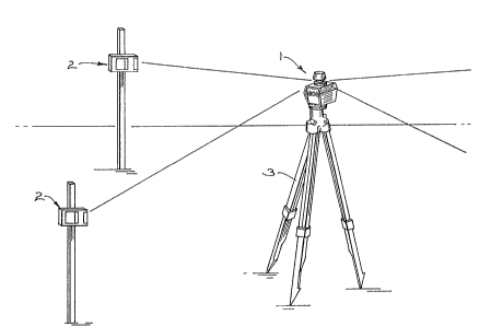
Fig. 1 is a pictoral view of a laser alignment system
which employs the present invention;
- Fig. 2 is a plan view of a receiver employed in the
system of Fig. l;
Fig. 3 is an electrical schematic diagram of the trans-
mitter employed in the system of Fig. l;
Fig. 4 is an electrical schematic diagram of the re-
ceiver employed in the system of Fig. l;
Fig. S are graphical representations of signals which
are produced in the system of Fig. l;
Fig. 6 are graphical representations of signals which
are produced in the receiver of Fig. 4;
Fig. 7 is an eIectrical schematic diagram of the band
pass filter which forms part of the receiver of Fig. 4;
Fig. 8 lS an electrical schematic diagram of the ampli-
fier and AGC circuits which form part of the receiver of
Fig. 4;
-4-
.~ . . ... .
~ti5~3
Fig. 9 is an electrical schematic diagram of the r~tio
compare and elevation decoder circuits which form part of the
receiver of Fig. 4; and
Fig. 10 is an electrical schematic diagram of the out-
of-level detector which forms part of the receiver of Fig. 4.
Referring particularly to Figs. 1 and 2, the laser
alignment system of the present invention includes a
transmitter 1 and one or more receivers 2. The transmitter 1
is supported on a rigid structure such as a tripod 3 and the
receivers 2 are carried around the construction site and used
where needed. The transmitter 1 contains a laser which
produces an alignment field in the form of a non-planar
reference cone which is formed by emitting coherent radiation
radially outward from the transmitter 1 in all directions.
When the transmitter 1 is level, this reference cone declines
from the horizontal in an amount sufficient so that due to
the curvature of the earth each point along the cone is an
equal dlstance from the earth's surface~ It has a thickness
of approximately five-eighths of an inch. For a more
detailed description of the mechanical and optical
construction of the transmitter 1, reference is made to co-
pending Canadian patent appIication Serial No. 517,014 filed
on August 28, 1986 and entitled "Self Leveling Transmitter
for Laser Alignment Systems".
Referring particularly to Fig. 2, the receiver 2 ls a
relatively small, hand-held device which includes a molded
plastic case 4 that supports a liquid crystal display (LCD) 5
and a photodetector module 6. The LCD 5 includes three
segments 7-9 which may be separately energized to indicate to
the operator that the receiver is positioned either above the
reference cone, on the reference cone, or below the
`;
.~ .
~. .
~;~65S~3
reference cone. The photodetector module 6 is rotatably
mounted between a pair of arms 10 and 11 so that it can be
oriented in a variety of positions to direct a pair of
photocells 12 and 13 towards the transmitter 1. The surfaces
of the photocells 12 and 13 are tapered to form triangular
shaped areas for receiving the energy produced by the trans-
mitter 1. As will be described in more detail below, when a
notch 14 in the case 4 is precisely aligned on the reference
cone, the signals produced by the two photocells 12 and 13
have the same magnitude. When the receiver 1 is positioned
slightly below the reference cone, the signal produced by
the upper photocell 12 is greater than that produced by the
lower cell 13. When it is raised slightly above the reference
cone, the upper cell 12 produces the larger signal. The
relative magnitude of these two signals is employed to
determine which LCD segment 7-9 is to be energized.
The receiver 2 includes other indicating devices. It
includes an audio transducer 15 which emits a sound when the
receiver 2 senses energy in the reference cone. A visual
indicator 16 is energized when the transmitter indicates
that the reference cone is not level. And finally, a visual
indicator 17 is energized when the receiver is turned on,
and an indicator 18 is energized when the battery voltage
drops below a preset value.
Referring paticularly to Fig. 3, the transmitter circuit
provides current to a laser diode 20 which emits coherent
ultraviolet radiation through a series of lenses, reflectors
and damping fluid to produce the laser non-planar reference
cone. The~laser diode 20 is packaged with a light sensitive
diode 21 that is positioned to sense the level of the energy
emitted by the laser diode 20. This energy is controlled by
.
~ ~ -6-
" - . .
a current regulator 22 which connects to the junction of the
diodes 20 and 21, and which controls the level of current
flowing through the laser diode 20 in response to a current
command signal applied to a control terminal 23.
The current regulator 22 forms part of a closed loop
power level control circuit which also includes an opera~
tional amplifier 24 and a power level reference circuit 25.
The power level reference circuit 25 produces a constant
reference voltage which is applied to the non~inverting
input of the operational amplifier 2~ and a feedback voltage
indicative of the level of the energy being emitted by the
laser diode 20 is applied to the inverting input of the
operational amplifier 24. This feedback voltage is produced
by the light sensitive diode 21 acting through a feedback
resistor 26. The reference voltage produced by the circuit
25 is preset to a value, which when combined with the feed-
back voltage at the amplifier 24, yenerates a command signal
for the current regulator 22 that results in the desired
power level from the laser diode 20. Typically, this power
level is set to the maximum r.m.s. power level allowed under
the applicable government regulations, and in prior systems,
this power is produced continuously.
One aspect of the present invention i5 to increase the
peak power produced by the laser diode 20 without increasing
the regulated r.m.s. power leveL which it produces. This is
accomplished by rnodulating the energy level of the laser
diode 20. More specifically, a modulation oscillator 30 is
connected to the control terminal 23 on the current reyulator
22 through a diode 31. The modulation oscillator 30 produces
a square wave voltage waveform which has a fifty percent
duty cycle. This modulation waveform alternately turns the
~7-
current regulator 22 on at its commanded level and fully
off. The modulation oscillator ~0 produces an~ one of thrse
frequencies (7.8 kHz, 8.0 k~z, 8.2 kHz) which is selectable
by closing one of three switches 32-34. In the followiny
description this modulation frequenc~ will be referred to as
8 kHz, although one of the other two frequencies may be
employed in any installation so as not to interfere with
other similar transmitters located at the sams site.
The primary purpose of the transmitter is to produce an
alignment field in the form of a non-planar reference cone.
To accomplish this a mechanism is provided which enables the
operator to manually adjust the level of the instrument.
And, as described in the above-cited copending patent appli-
cation, once the instrument is brought to within 10 arc
minutes of perfect level, an automatic leveling system
provides the final adjustment. It is imperative, of course,
that this level be maintained at all times, as considerable
damage can be done if grading or construction work proceeds
in reliance on an alignment which is out-of-level.
While maintenance of level cannot be insured, the pre-
sent invention does provide an immediate indication of an
out-of-level condition. Referring again to Fig. 3, an
out-of-level detection circult 40 is provided at the trans-
mitter 1 and it produces an out-of-level signal on lines 41
and 42 when thé transmitter 1 is not within the ranye of its
automatic leveIing mechanism. The signal on line 41 is
input to a driver circuit 43 which produces a signal suit-
able for driving a light emitting diode 44. The light emit-
ting dlode 44 is energized when an out-of-level condition is
sensed and a visual indication is provided to those working
in the vicinity of the transmitter 1.
,
-8-
~, ., ~ -, -, ,
~ , :
.',~ ~' ', .
:
923
An out-of-level condition i6 also indicated to operators
using the receivers 2. This is accomplished b~ further
modulating the energy produced by the laser diode 20. More
specifically, a 2.68 ~ertz oscillator 45 is coupled to the
non-inverting input of the operational amplifier 24 through
a switching transistor 46. When the out~of-level signal is
produced on line 42, this square wave is applied to the
amplifier 24 to repeatedly turn the current control circuit
on and off at the 2.68 ~ertz rate. As will be described
below, this condition is detected at each receiver 2 and a
visual indication is produced.
Referring still to Fig. 3, there are numerous methods
for detecting an out-of-level condition. In one preferred
embodiment of the invention two photodetector diodes 60 and
61 are mounted within the transmitter 1 and energy emitted
by the laser diode 20 is reflected off a conical surface
onto them. The conical surface produces a ring of energy
which impinges on both diodes 60 and 61 when the transmitter
1 is level. When out-of-level, the conical surface swings
relative to the diodes 60 and 61 and the ring of energy
moves as well. As a result, one or both of the diodes 60 or
61 does not produce current when an out-of-level condition
occurs. For a more detailed description of this aspect of
the out-o-level detector, reference is made to the above-
cited copending patent application which is incorporatedherein by reference.
In a second preferred embodiment of the invention a
single photodetector diode 60 is mounted within the trans-
mitter 1 and energy emitted by the laser diode 20 is re-
flected off a planar surface formed on the bottom of theleveling cone contained therein. When the transmitter is
.. .. ~. .
.
~Z~S~3
out-of-level, this reflected energy does not strike the
surface of the photodetector diode 60 and it does not produce
current.
The currents prorluced by each photodetectiny diode 60
and 61 are amplified and filtered by an operational ampli-
fier 62, and are compared with a reference current in opera-
tional amplifier 63. When sufficient eneryy impinyes on the
diode 60 and 61, the output of the amplifier 63 is a low
voltaye which is input to an operational amplifier 64. The
positive feedback around the amplifier 64 causes it to
saturate at the negative power supply voltage. If the
outputs of both amplifiers 64a and 64b are low, no base
current is provided to a pair of switchiny transistors 65
and 66 and they are turned off. On the other hand, if
insufficient eneryy impinges on either photodetector diode
60 or 61, the output of its associated operational amplifier
64a or 64b is saturated at a hiyh voltage and base current
is supplied to the switchiny transistors 65 and 66. As a
result, out-of-level siynals are produced on the lines
and 42 and the condition is indicated to the operator as
described above. Of course, if only a single photodetector
diode 60 is employed, as described above, the circuitry
associated with the photodetector diode 61 is not required
and the~output of operational ampli~ier 64a is sufficient to
operate the~switching transistors 65 and 66.
Waveforms which illustrate the energy produced by the
tranSmltter 1 are shown in Fig. 5. Waveform 70 illustrates
the energy which is produced in the laser alignment reference
cone under normal operating conditions, and waveform 71
lllustrates the pulsating energy which is produced when an
out-of-level condition exists. It should be apparent to
~ ' -10-
:
~5~
those skilled in the art that information other than an
out-of-level condition may be encoded into the energy which
is projected into the laser alignment reference cone. ALso,
other techniques may be employed to encode the information.
Referring particularly to Fig. 4, each receiver 2 in-
cludes circuitry for detecting and indicatiny the precise
location of the laser alignment reference cone. Separate
signal channels are provided for each photocell 12 and 13,
and common elements in each will now be described using the
same reference numbers. The signal produced by the photo-
cell 12 or 13 is applied to the input of a band pass filter
100. An inductor 101 is connected across the inputs of the
band pass filter 100, and it provides a low impedance path
which shunts the d.c. and low frequency a.c. components of
the input signal. The band pass filter 100 passes a narrow
band of signal components centered about the 8 kHz modulation
frequency. It also provides amplification for those signal
components, and as a result, signals produced by ambient
light and by noise energy are substantially reduced relative
to the signal produced by the energy in the alignment refer-
ence cone.
The output of the band pass filter 100 is applied to an
amplifier 102. Because the receivers 2 may be used at
various distances from the transmitter 1, the strength of
the signal produced by the modulated laser energy will vary
~; considerably. Accordingly, the gain of the amplifier 10~
may be swltched automatically by an automatic gain circuit
(~AGC) 103 to provide the appropriate amount of amplification.
As shown by the waveorm 104 in Fig. 6, the output of the
ampl~ er 102 is a voltage which swings between zero volts
and a positive voltage at the modulation fre~uency. The
-`
~ ,
.j , . .
lZ~i5~3
magnitude of the positive voltage is proportional to the
laser energy which impinges the photocell 12 or 13 The
gain of the amplifier 102 is adjusted to prevent it from
being driven into saturation.
Referring again to Fig. 4, the output of the amplifier
102 is applied to an auto correlator circuit r~hich is indi-
cated by the dashed line 105. The auto correlator 105
includes an analog switch 106 which is turned on in synchronism
with the 8 kHz signal by logic signals received through a
control line 107. As a result, the level of the 8 kHz
signal is sampled at its peak value. An RC filter 108 at
the output of the switch 106 maintains a relatively uniform
voltage level (V) which follows the sampled value of the 8
kHz signal. The control signal which synchronously operates
the analog switches 106 is shown in Fig. 6 as the waveform
109, and the output of the auto correlator 105 is indicated
by the dashed line 110.
As will be described in more detail below, the voltage
levels Va and Vb at the outputs of the auto correlators 105a
20 and 105b are applied to the AGC circuit 103 where they are
summed and employed to determine the gain required at the
amplifiers 102a and 102b. These same signals, Va and Vb,
are aIso applied to the inputs of a ratio comparator circuit
111 where their relative magnitudes are compared.
The ratio comparator 111 determines the position of the
receiver 2 relative to the laser alignment reference cone
and produces a corresponding logic level signal on one of
four output ~lines 112-115. These signals are applied to an
elevation decoder 116 which converts them to logic level
signals that indicate whether the receiver 2 is below the
alignment reference cone (L0), at the level of the alignment
-12-
,
,~
12ti5~
reference cone (ON); or above the aliynment reference cone
(HI). These signals are produced at respective outputs
117-119 when an enable signal is received on a control line
120.
The three elevation decoder output signals (LO, ON and
HI) are applied to an audio driver circuit 121, an LCD
driver circuit 122 and a set of three remote buffers 123.
The audio driver circuit 121 receives three audio signals
having different frequencies, and one of these is applied to
the audio transducer 15 in response to the respective signals
LO, ON and HI. Similarly, the LCD driver 122 energizes one
of the LCD display elements 7, 8 or 9 in response to these
same signals, and the remote buffers 123 condition the
signals so that they can be sent over conductors 124 to a
remotely located indicator module.
It should be apparent that many other methods and
devices may be employed to indicate the position of the
receiver 2 and to assist the operator in finding the center
of the alignment reference cone. In addition, the signals
produced by the elevation decoder 116 may be employed as
part of~a servo-mechanism which automatically maintains the
receiver 2 in the laser alignment reference cone and which
automatically controls the level of a blade or other earth
moving implement on construction equipment.
Referring still to Fig. 4, the receiver 2 does not
lndlcate the presence of the laser alignment reference cone
untlI it senses and "locks" on the 8 kHz signal produced at
the output of the amplifiers 102a and 102b. To accomplish
this these signala are coupled to the input of an operational
:.
ampllfier 130 where they are summed and input to a phase-
locked loop circuit 131. When in its free-running state the
~ -13-
,
~;~6~3
phase-locked loop 131 produces a 500 kHz siynal at its
output 132 and this is re~uced to an 8 kHz siqnal by a
counter 133 which operates as a divider. The counter 133
may also be chanyed by groundiny either of two terminals 134
or 135 such that the frequency at its output 136 i9 set to
7.8 kHz or 8.2 kHz to accommodate transmitters which are
operated at these alternative modulation frequencies.
The output of the counter 133 is fed back to a compari-
tor input on the phase-locked loop 131, and when the input
signal from the operational amplifier 130 has the same fre-
quency, and phase, the phase-locked loop 131 locks onto the
input signal and produces a corresponding, synchronized
signal at the counter output 136. This synchronized signal
is indicated as waveform 137 in Fig. 6 and it is applied to
a phase shift circuit 138 which produces a similar waveform
139 that is shifted 90 degrees in phase.
The phase shift circuit 138 forms part of a quadrature
detect system that also includes a second phase-locked loop
140 and an operational amplifier 141. The output of the
phase shift circuit 138 is compared with the received signal
from the operational amplifier 130, and a voltage is produced
at an output 142 on the phase-locked loop 140 which is prc-
portional~to their instantaneous phase difference. This
voltage is zero when the signals are in phase, and it is a
maximum when the signals are 90 degrees out of phase. When
the voltage output is at a maximum, it is an indication that
the first phase-locked loop 131 has locked onto the 8 kH2
signal~produced by the modulated laser energy. The opera-
tional ampIifier 141 operates as a voltage comparator which
- 30 produces a logic high "lock" signal when this occurs. The
output of the phase-locked loop 140 is averaged ~y an RC
-14-
. .
~26~
filter 143 at the input of the operational amplifier 141 to
prevent momentary signals from produciny a lock indication.
When the phase-locked loop 131 is locked onto the 8 kHz
signal, the output of the counter 133 is applied to a pulse
generator 150 and it produces the control signal on the line
107 which synchronously operates the analog switches 106a
and 106b. The "lock" signal produced by the operational
amplifier 141 is applied to the set terminal on a J-K flip-
flop 151, which is set and produces the enable signal for
the elevation decoder 116 through a NAND gate 152. Thus,
when the 8 kHz signal is detected, the phase-locked loop 131
begins producing a synchronous signal ~hich is used by the
pulse generator 150 to properly operate the synchronous
level detectors 105a and 105b. Thus, by the time the "lock"
signal is produced and the elevation decoder 116 enabled,
accurate position information is available for display.
When the 8 kHz signal is lost, the phase locked loop
131 becomes free running and the logic high "lock" signal
produced ~y the operational amplifier 141 is terminated.
The J-K ~lip-flop 151 is reset by the next pulse which ap-
pears at the output of the counter 133, and the elevation
decoder 116 is disabled so that no further audio or visual
indications are provided. This free running state continues
until the 8 kHz modulation fre~uency is again detected in
the signals produced by the amplifiers 102a and 102b.
The "lock" signal produced by the ~uadrature detect
circuit also serves as the input to an out-of-level detector
153 and it lS applied to a remote indicator module through a
line 158. The "lock" signal is inverted by a gate 154 and
is emp1oyed to detect when the 8 kHz alignment plane laser
energy is being pulsed at the 2.68 Hz rate. As explained
:
~ -15-
:. - . ~ ., ,
~2~ 3
above, this indicates that the transmitter 1 is out-of-level
and that the alignment information should not be used. ~en
this occurs an output 155 on the out-of-level detector 153
is driven low and the out-of-level indicator 16 is thereby
energized to warn the operator of the condition. In addi-
tion, the NAND gate 152 is disabled through a control line
156 so that the elevation decoder 116 and the indicating
devices which it controls are rendered inoperable for the
duration of the out-of-level condition.
The "lock" signal which indicates the out-of-level
condition is shown as waveform 157 in Fig. 5. As will be
described in detail below, two consecutive out-of-lock indi-
cations of the proper duration are required to signal an
out-of-level condition. The condition terminates whenever
the receiver 2 locks or unlocks for a period longer than two
consecutive 2.68 Hz cycles.
Referring particularly to Figs. 4 and 7, the band pass
filter circuit 100 is comprised of five operational ampli-
fiers 170-174 which are commercially available in integrated
circuit form. The amplifier 17n operates as a pre-amplifier
with a frequency response in the range from 200 to 20,000
Hertz and a gain at the 8 kHz modulation frequency of 25.
The amplifier 171 is a low pass filter with a cut off fre-
quency of 9 kHz, and the amplifier 172 is a high pass filter
whlch has a cut off frequency of 5.7 kHz. The amplifier 173
:. .
is connected as a high pass filter with a cut off frequency
of 4.3 kHz, and the amplifier 174 provides a gain of two to
the narrow band of frequencies about the 8 kHz modulation
frequency.
It should be apparent that numerous circuits for provid-
ing amplification and band pass filtering in the audio fre-
-16-
,,
' .
~S~3
quency range are known to the art The choice of an 8 kHz
modulation fre~uency is not, however, 50 apparent. It has
been discovered that many fluorescent liyhts found in the
work place and used outdoors produce light energy which is
modulated in amplitude. The magnitude of this modulated
ambient light begins to drop off rapidly at approximately 4
kHz and is relatively insignificant at 8 kHz. In addition,
8 kHz is well within the frequency range of low cost and
readily available linear integrated circuit components.
Referring particularly to Figs. 4 and 8, the AGC cir-
cuit 103 is constructed around three operational amplifiers
180-182. The amplifier 180 operates to sum the two signals
Va and Vb which are output by the level detectors 105a and
105b. If the sum of these signals is less than .48 volts,
the output of operational amplifier 182 rises to a logic
high voltage, and if their sum is grea-ter than 1.2 volts,
the output of operational amplifier 181 rises to a logic
high voltage. The output of amplifier 182 drives an UP
count line which decreases the gain of the amplifiers 102a
and 102b, and the output of amplifier 181 drives a DOWN
count line which increases the gain of the amplifiers 102a
and 102b.
Referring still to Fig. 8, the amplifiers 102a and 102b
each include a 4-bit up/down binary counter 190 which is
drlven by the UP and DOWN control lines through respective
~NAND gates 191 and 192. The counter 190 connects to a set
of four resistors 193 which are connected in parallel with a
gain resistor 194. The gain resistor 194 operates in combi-
nation with a feedback resistor 195 to determine the gain of
an operational amplifier 196. When the counter 190 is at
its maximum count, the gain of the amplifier 102 is at its
-~7-
.. ~ . . . ~ .
~2~iS~
minimum of one. The counter 190 may be counted do~n in
sixteen steps to proyressivel~ add the resistor~ 193 in
parallel with the resistor lg4 and to thereby progressively
increase the gain to its maximum. The counter 190 is counted
up or down in synchronism with a 500 Hz clock signal applied
to the AND gates 191 and 192.
Referring particularly to Fiys. 4 and 9, the ratio
comparator 111 is formed around four operational amplifiers
200-203 which are connected to receive the respective signals
Va and Vb at their differential inputs. The amplifiers
200-203 are operated as voltage comparators and the values
of the resistor networks connected to their non-inverting
inputs establishes the ratio of the input voltages Va/Vb
which will cause them to switch state. When the voltages Va
and Vb are substantially the same, the outputs of all the
amplifiers are saturated at a logic low voltage. As the
magnitude of voltage Va becomes less than Yb, a first thres-
hold is reached (Va/Vb = .866) at which the output 113 of
operational amplifier 201 is driven to a logic high voltage.
If the ratio Va/Vb continues to decrease, a second threshold
is reached (Va/Vb = .75) at which the output 112 of opera-
tional amplifier 200 is driven to a logic high voltage.
Similarly, if the magnitude of voltage Va increases above
that of Vb, first the output 114 of amplifier 202 rises to a
logic high voltage (Va/Vb = 1.133) and then the output 115
of~amplifier 203 rises (Va/Vb = 1.25).
The signals produced on the outputs 112-115 are clocked
into four D-type flip-flops 205-208 in the elevation decoder
116. A 30 Hz clock is employed for this purpose. A set of
~ive NAND gates 209-213 connect to the outputs of the flip-
flops 205-208 and their outputs are combined by a set of
~ -18-
S9~Z3
three NOR gates 214-216 to produce the three cutput aignals
"LO", "ON" and "HI". These three output signals are gated
onto the lines 117-119 when the enable line 120 is at a
logic high voltage as described above.
It should be apparent that although the preferred
embodiment of the receiver 2 provides only a three-state
indication of position rela-tive to the laser alignment
plane, five-state position information is available at the
output of the NAND gates 209-213. This additional informa-
tion may be useful, for example, where the receiver 2 is
used in connection with a servomechanism for controlling the
elevation of an excavator blade or the like.
Referring particularly to Figs. 4 and 10, the out-of-
level detector 153 includes a counter 220 which is reset
each time the 8 kHz modulated laser energy is lost. As
described above, this condition is indicated by the LO~K
signal on line 221. The inversion of this signal is also
employed to clock two J-K flip-flops 222 and 223 when the 8
kHz signal is again detected. The counter 220 is advanced
by a 62 Hz clock signal, and at 100 milliseconds after
termination of the 8 kHz signal, a first output 224 goes to
a logic high to set an R-S fllp-flop 225. The flip-flop 225
is reset 170 milliseconds later when an output 226 on the
counter 220 goes to a logic high. The counter 220 operates
in comblnation with the flip-flop 225 to define a time
wlndow whlch lasts from 100 to 270 milliseconds afte~ the 8
kHz signal is lost. If the 8 kHz signal is re-established
during~this time window an out-of-level condition may be
indicated. This event iæ clocked into the J-K flip-flop 222,
and if the~same sequence repeats after the 8 kHz signal is
~ again lost, then the J-K flip-flop 223 is set and an out-of~
., : ~ -19-
'`,
" , , - ,: . ,
.. . .. .
~2~ 3
level condition is indicated at the OutplltS 155 and 156.
The operation of the ~-S flip-flop 225 is illustrated in
Fig. 5. The waveform indicated by the solid line 227 sho~Js
the R-S flip-flop 225 when it is reset by the "lock" siynal
157, and the dashed line 228 indicates the total exten'c of
the window.
The out-of-level condition is maintained as lony as the
8 kHz signal is received and lost at the 2.68 Hz rate If
this rate is not maintained during one cycle, the J-K flip-
flop 222 is reset, but the J-K flip-flop remains set and the
out-of-level indication is maintained. However, if the rate
is lost for two consecutive 2.68 Hz cycles, then the J-K
flip-flop 223 is also reset and the out-of-level indication
is terminated.
It should be apparent to those skilled in the art that
many of the discrete circuit components disclosed herein may
be implemented as a custom or semi-custom integrated circuit,
or the functions which they perform may be implemented with
a properly programmed microcomputer. These and other varia-
-tions are possible without departing from the spirit of the
in~ention~which is defined in the following claims.
:
-20_