Note: Descriptions are shown in the official language in which they were submitted.
--1--
BACIiGROt~ND OF THE INVENTION
This application concerns an electron beam memory
system with improved high rate digltal beam pulsing
system. The memory system has an electron gun capable
5 of developing high enough electron probe current
densities to permit no-develop recording and small
enough probe sizes to permit ultra-high densi-ty
recording, yet of such low mass and compac-tness as to
make feasible rapid random accessing of any area on the
system's recording medium~
In the context of such a system, beam pulsing
apparatus is needed which is compa-tible with and
contributes to the achievement of these capabilities in
the gun.
Electron beam digital pulsing systems are known
which create an intermediate beam cross-over or focus
between the source and ultimate probe (focus). A
simple deflector is placed at the location of this
intermediate focus and a suitable aperture is put into
the succeeding lens. When the deflector is activated,
the beam strikes the aperture support and is thereby
attenuated. The beam, when undeflected, passes through
the aperture unattenuated, the ultimate focus being
unaffected.
The net result is that the recording beam can be
turned off and on ~pulsed) without being deflected
sideways or becoming distorted. This is an effective
way to pulse an electron beam, bu-t requires a second
lens -- a constraint which all but rules it out as a
feasible beam pulsing technique in a system of the type
--2--
described in which gun compactness and low mass are of
critical importance.
It is known in a scanning electron microscope
system having a magnetic focus lens to add an auxiliary
magnetic lens or an auxiliary winding on a main focus
lens, and to apply, when working in a high resolution
mode, a current pulse to the auxiliary winding or lens
to selectively defocus the electron beam. See U.S.
Patent No. 3,919,500. The described technique is not
used to apply pulse information. Rather, the defocused
condition of the beam is used to develop a total-beam-
current reference which is used to compensate the
resultant data for instability in the beam current.
This scanning electron microscope technique would
not be suitable for use in the electron beam memory
system with which this invention is concerned, as the
additional lens or winding would unacceptably add to
the mass and bulk of the electron gun. Further, the
inductance of the auxiliary lens or winding would
unacceptably limit the achievable data recording rate.
U.S. Patent No. 3,748,467 discloses a scanning
electron microscope with an auxiliary lens which is
switched between two current levels to create -two fixed
focal planes, the da-ta gathered from which planes are
displayed on separate cathode ray tubes. ~gain, the
technique is not used for pulse information recording
and would be similarly unacceptable for that purpose
for the same reasons.
An auxiliary magnetic lens of the type called for
in the afore-discussed patents is disclosed in U.S.
Patent No. 4,245,159.
2~
~ .S. Patent No. 3,397,959 discloses a scanning
electron microscope utilizing an auxiliary focus lens
in an automatic focusing systern for the microscope.
OBJECTS OF TFIE IraVENTION
It is an object of this invention to provide
apparatus for high rate pulsing of an electron beam in
an electron beam memory system.
It is another object of this inven-tion to provide
such digital beam pulsing apparatus which adds no
significant mass or bulk to the electron gun, and which
permits very high recording rates.
It is another object to provide such high rate
digital beam pulsing apparatus which is useful with a
high electron density recording system and is low in
manufacturing cost.
It is still another object to provide such high
rate digital beam pulsing apparatus which is suitably
adapted for use with an electron gun having ei-ther
magnetic or electrostatic main focus lens means.
It is yet another object to provide in an electron
beam memory system having an electron gun with a ~ield
emission source, improved apparatus for monitoring the
source heater current.
E'~RIEF DESCRIPTIOl~ OF THE DRAWINGS
FIG.1 is a highly schematic illustration of an
electron beam memory system incorporating a high rate
~L2~12~2
--4--
digital beam pulsing sys-tem constructed according to
t~ teachings of the present invention;
FIG. 2 is a sectional view of a wri-ting head
constituting part of the FIG. 1 sys-tem; and
)
FIG. 3 is a schematic dia~ram illustrating the
beam pulsing and source heater current monitoring
system according to this invention and Fig. 3a being a detai l
of Fig. 3.
escr ption o~ the Preferred Embodiment
FIG. 1 is a schematic view of an electron beam
memory system 10 embodying the present invention.
Before describing in detail the high rate digital beam
pulsing and source current monitoring systems according
to the present invention, the general aspects of the
FIG. 1 electron ~eam memory system embodying the
invention will be discussed. The FIG. 1 system 10 is
shown as including a vacuum enclosure, depicted
schematically in dotted line form at 12. Within -the
enclosure is a storage medium 13 supported on a
rotatable disc 14. The disc 14 is rotated by a disc
drive shown schematically at 16.
he electron beam memory system 10 includes a
plurali-ty of electron beam heads adapted for
simultaneous operation. In the illustrated embo~iment,
I have shown three heads -- a writing head 18
containing an electron gun for assisting in recording
information, a verification head 19 containing an
electron gun for assisting in verifying the fact and
inte~rity of the stored information, and a reading head
20 containing an electron gun for assisting in
retrieving the stored information.
-
The electron beam memory system 10 is illustratedschematically as including head drives 21, 22, 23
interconnected with the heads 18, 19, 20 by support
arms 24, 25, 26 for moving the heads ~8, 19, 20 across
the disc 1~.
~ uxiliary electronic and electrical appara-tus,
shown schematically at 27 provides -the necessary clrive
signals through conductors 28, 29, 30 for energizing
head drives 1, 22, 23.
Apparatus 27 also supplies through conductor 31
suitable drive currents for the focus lens, hea-ter
current for the field emission source heater and
energization poten-tials for the gun elec-trodes through
bundles of conductors 33, 34, 35.
FIG. 2 illustates a-writing electron gun contained
within writing head 18. As will be described, the FIG.
2 gun is capable of developing a finely focused
electron beam probe at high beam current densities, yet
is ultra-compac-t and of extremely low mass. The
electron gun makes possible a random accessed electron
beam memory system for high rate, ultra-high density
electron beam data recording, and yet with recording
power making possible no-develop recording, i.e.,
recording without the need for developing the recording
medium after exposure. With such a writing electron
gun, a very high capacity electron beam storage medium
can be employed using multiple accessory verification
and reading heads to permit simultaneous reading and
reading over long periods of time -- a cri-tically
importan-t capability for a great many applications.
Because of the vast storage capability of an electron
--6--
beam memory system such as this, it may be totally
impractical in many applications -to delay access to the
memory until the memory is filled (which could take
weeks or months), during which time the stored
information is inaccessible.
~ n electron beam memory system becomes truly
universally useful only when i-t has the capability to
record without any development of the medium using a
! rapid random accessing head and wi-th simultaneously
o~erable pick-up heads for verifying and/or retrieving
the stored information as soon as it is recorded.
Before engaging in a detailed discussion of the
FIG. 2 electron gun, I will first discuss in general
terms the performance re~uirements imposed on a writing
gun of an electron beam memory system of the character
; used herein. A few of -the performance, packaging and
other requirements imposed on the gun are, in general
- terms, as follows: ~1) as stated, the gun must be of
sufficient compactness and of sufficiently low mass as
to be readily capable of being rapidly accelerated and
decelerated to effectuate a rapid random accessing of
the electron beam memory medium; (2) the gun must be
capable of producing an extremely fine probe to permit
ultra-high density recording on the medium; ~3) the
prohe produced must not only be extremely fine, but
must have high current densities, in order that no-
develop recording can be achieved -- that is, recording
characterized by an alteration of the physical state of
the recording medium which can be detec-ted immediately
after recording, as by use of an electron beam probe;
(4) the gun must be capable of working with relatively
low accelerating voltages in order -that the beam
penetration and spreading is not excessive, and so that
the insulation requirements do not drive up the size
and mass of the gun; (5) the head must have a modest
power consumption in order that massive cooling
structures are not required; ~) the gun must have an
electron source which not only is extremely bright, bu-t
is also stable and of ~ong life in order that-the
system in practice is easy to use by operators of
ordinary skill; and (7) the gun must have a
commercially tolerable cost of manufacture.
The simplest way to effec-t an irreversible change
in the physical sta-te of the recording medium is to
induce melting or boiling of the recording material to
create a depression or pi-t in the medium. The pit can
be detected, for example, with a less-intense electron
beam probe and accompanying means for detecting
secondary, back-scattered or transmitted electrons.
The melting temperature "Tm" of a material can be
approximated by the relation TM =~ , where
"I" is the electron beam current in amperes, "V" is the
beam voltage in volts, "K" is the thermal conductivity
of the material in calories per centimeter squared per
second, and "a" is the radius of the heated zone in the
recording medium in centimeters.
~ lsing bismuth as the recording medium, for
example, having "K" = .02 and "Tm" = 270 degrees
centigrade, and assuming a beam voltage "V" of 5
kilovolts and a heated zone "a" of .08 microns, then
"I" = 160 nanoamperes. In this example, a curren-t "I"
of 160 nanoamperes and a heated zone "a" of .08 microns
establishes a current density threshold above which -the
melting point of the bismuth recording medium is
exceeded and "no-develop" recording can be achieved.
--8--
In the present invention, as will be described in more
detail below, digital recording is achieved by the use
of a pulsed recording signal to create "pits" or "no-
pits", signifying binary "l's" or "O's" (or "Ols" and
"1's") in the recording medium.
Recording rates are limited by the rate at which
the medium can be heated: Y=P a2, whexe ~ is
the specific heat and p is -the density of the
material. The recording rates for most materials and
the probe diameters of interest is in the order of
to seconds, allowing recording rates of 100
megahertz and above.
In terms of beam power requirements, for beams
having current values in the range of 100-500
nanoamperes with accelerating voltages of 3-5
kilovolts, for example, the beam power is in the range
of 300-500 microwatts. This is more than adequate
power to produce melting in materials of interest such
as bismuth, tellurium, arsenides of such materials and
mixtures thereof, for example, which require only a few
microwatts of power to be melted, using probes with a
diamter of .1 micron or less.
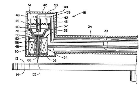
~ detailed discussion of the FIG. 2 electron gun
will now be engaged. In order to achieve the high
current densities required for high rate, no-develop
recording, a heated field emission ca-thode is employed.
In FIG. 2, the field emission source -tip is shown
at 38. A tip can is shown at 40 and heater leads at
42, 43. Silica ball 44 supports the heater in can 40.
The tip may be operated at vacuum levels of to
torr, for example. Source currents up to 1,000
-8A-
microamperes can be produced. Emission noise levels
fol~ these operating parameters are in the order of a
few percent.
An insulator 46 supports the tip assembly
comprising the can 40 and tip 3~ and isolates it
electrically from the other par-ts of the gun and the
gun enclosure 48. The insulator 46 is, in turn,
supported by a support element 49.
In order to draw elec-trons from the tip, the FIG.
~ ~un includes a truncated conical accelerating anode
electrode SO which is spaced from a beam tube assembly
52 by an insulating ring 57. Electrically conductive
hold-down pins 51, 53 hold such electrode 50 agains-t
ring 57. Appropriate electrical potential is applied
to electrode 50 through lead 59.
A focus lens 54 has a single lens coil 56 and is
positioned a relatively short object distance from the
tip 38 for receiving a beam of elecrons from the anode
electrode 50. The focus lens 54 forms a finely focused
~0 electron beam probe 55 (the beam focus) on the medium
10 at a relatively short focal distance therefrom. The
sum of the object and image distances are so small as
to s~lppress the space charge contribution to probe
diameter and thereby to make feasible electron beam
~5 probes with diameters as small as a few angstroms.
Located within the compass of the coil 56 are
interwound stigmator coils 58 for reducing to an
acceptable level any astigmatism which may be present
in the electron beam. Axially separated from -the
stigmator coils 58 are a pair of in-terwound deflection
coils 62 for deflecting the electron beam in orthogonal
- 9 -
directions across the medium 13. Gross positioning of
t`~e electron beam probe 55 is by movemen-t of the head
18 across the storage medium 13. Fine positioning of
the electron beam probe 55 on the storage me~ium 13 is
accomplished by appropriate selection of driviny
currents for the deflection coils 62.
A beam tube 66 ex-tends from the anode electrode 50
to the point of beam exit from the gun 36.
The electron beam memory system is very small with
a total overall length from source tip 33 to probe of
no greater than about 5 centimeters. The operating
voltage of the electron gun will be in the range of
about 3 to lOoKv, the probe size will be in-the range
of 100-500 A with a probe current in the range of
100-500 nA. This will allow a writing speed of 100 MHz
or more. The electron gun preferably has a total mass
of no more than about 200 grams. The electron gun 36
is extraordinarily compact; by way of illustration, the
total length of the gun is no more than about 4
centimeters. A gun having such extreme compactness and
low mass can be quickly moved to any part of the
recording medium in order to effectuate rapid random
accessing of any selected area on the medium for the
purpose of adding information to any selected file or
~5 area on the medium.
Important aspects of the present invention will
now be described. In general terms this invention
concerns an electron beam memory system which includes
a substrate mounted for rotation and supporting an
information storage medium. Means are provided for
rotating the substrate. An electron gun and means for
effecting relative movement between the gun and the
~10--
subs~rate are provided. The electron gun in the system
of the present invention comprises a cathode, anode
means and means for developing and applying between the
cathode and the anode means a predetermined
accelerating potential for forming a high brightness
electron source and for causing an electron beam to be
formed through the anode means. A focus lens is
provided for receiving the beam and for forming a small
yet intense electron beam probe a-t a predetermined
: 10 first focal distane from the lens means. A high rate
di~ital beam pulsing system is provided which includes
voltage pulse generating means for developing a series
of voltage pulses of predetermined magnitude and
duration. Means are provided for applying the pulses
to the gun such that the pulses add to or substract
from the accelerating potential thereby causing the
focus lens to focus the beam at a predetermined second
focal distance differing from the first focal distance.
The gun is positioned relative to the recording medium
such that one of the first and second focal distances
corresponds to the distance between the focus lens and
the recording medium.
As noted, this invention is adapted for use in a
rapid random accessed electron beam memory system with
a no-develop recording medium -- in particular, a
medium such as bismuth or other material having a
relatively low thermal conductivity. Such media can be
melted or evaporated by the application of a relatively
moclest level of electron beam energy. The temperature
rise in such recording media is proportional to the
bombarding electron current level and inversely
proportional to the radius of the bombarding electron
beam probe. The beam pulsing system of the present
invention causes a rapid change in the temperature of
the localized areas on a recording medium by effecting
t~apid changes in the cross-sectional area of the
electron beam which intercepts the medium. This chanye
in beam intercept area is accomplished by altering the
5 focal distance of -the focus lens.
As noted, this invention is most suitable for use
with an electron gun having a field emission source.
It is a characteristic of a field emission gun-that the
! energy of the electrons drawn from the field emission
tip is determined by the accelerating voltage applied
between the anode electrode and the tip. If the
accelerating voltage is adjusted between first and
second levels, the focal distance of the lens will
change correspondingly between first and second focal
distances. For an accelera-ting voltage of a few
thousand volts, a small change in the order of 10 to 20
volts will effect a significant change in the focal
distance of the focus lens and thus in the intercept
area of the beam on the medium 13.
As noted, in accordance with this invention,
voltage pulses are applied to the gun such as to add to
or subtract from the accelerating potential and thus
` create the aforesaid two levels of accelerating
potential and two different focal distances. Applying
pulses corresponding to digital information to be
recorded, the focal distance can be changed at digital
recording rates. If the recording medium is located at
one of the two focal distances, the probe will he in
focus on the medium for one pulse level and out of
focus at the other pulse level.
In accordance with this invention, a recording
medium is selected which has a melting characteristic
-12-
which is such that when the medium is bombarded by an
electron beam having a current density exceeding a
predetermined melting threshold, melting of the medium
occurs. The said curren-t density of the electron beam
and the magnitude of the voltage pulses are caused to
be such that when the beam is focused on the medium,
the melting threshold of the medium is exceeded and
melting of the medium occurs, but when the beam is
focused at the other of the focal distances and is thus
out of focus with respect to -the medium, the threshold
.is not reached and melting of the medium does not
occur.
It is highly desirable in a practical electron
beam memory system, due to the immense amount of
information to be stored, that digital recording be
effective at very high rates -- for example, in the
order of 100 megahertz. That requirement implies that
capacitance in the system applying the voltage pulses
be minimized.
It is another aspect of this invention to provide
in a digital beam pulsing system of the character
described means for applying the aforesaid voltage
pulses in additive tor subtractive) relationship to the
field emission gun's accelera-ting potential in such a
2S way that the pulse generating apparatus can be
maintained at ground potential or some other relatively
low potential, and thus can be manufactured at
relatively lower cost than if such apparatus were
maintained at accelerating potential.
It is still another aspect of this invention to
provide a high rate digital beam pulsing system which
is relatively low in cost. In field emission guns the
-13-
stability of the heater current must be extreme. This
re(luires that the heater current be carefully monitored
and controlled. The cost of field emission guns has
been high due in part to the need for moni-toring and
control equipment which, in the past, has been
maintained at the accelerating po-tential of -the gun --
typically in kilovolts or even tens of kilovolts. As
t~ill be e~plained in detail below, in accordance with
an aspect of this invention, only the current supply, a
current sensor, and certain other minor elements are
maintained at the accelerating po-tential, the heater
current stabilizing system being maintained at ground
or other relatively low potential.
FIG. 3 il lustrates in detail the high ra-te
digital beam pulsing system of this invention. In FIG.
3 the electron gun 36 is shown as developing an
electron beam 68 focused to form a probe 55 on the
recording medium 13 at a focal distance FD1 (focal
distance 1). The beam 68 is shown in dotted lines in a
second state corresponding to application of an
accelerating potential at a greater level. In the
second state the probe 69 is focused at a second focal
distance, designated FD2 in FIG. 3.
i
In accordance with this invention, there is
applied to the electron gun, in such a way as to add to
or subtract from the gun's accelerating potential, a
series of voltage pulses characterizing the digital
information to be recorded. This series of pulses
causes the focal distance of the focal lens 54 to vary
between focal distance FD1 and focal distance FD2 at
the digital information recording (pulse) rate.
When the beam is focused at focal distance FD1,
-14-
that is with the probe in focus on -the medium 13, the
e ectron beam has a current density which exceeds a
predetermined melting threshold of the medium and a pit
or hole 70 is formed in medium 13. Conversely, when
the voltage pulse is at its alternate eleva-ted state,
the energy of the electrons in the electron beam is
increased and the probe is focused at focal dis-tance
FD2 with the result that the area of intercept or
impingement of electron beam 68 expands to have a
radius "a" (FIG. 3) which is sufficiently greater than
the radius of probe 55 that the melting threshold of
the medium ls not reached and melting of the medium
does not occur -~ that is, not pit or hole is formed in
the medium when the beam is focused at focal distance
FD2.
The high rate digital beam pulsing system of this
invention will now be described in more detail. In
FIG. 3 there is shown a high voltage supply depicted
schematically at 72. Acceleration voltage is applied
to the field emission tip 38 by a D.C. voltage source
73. A first series of voltage pulses corresponding to
the digital information to be recorded is generated at
ground or a relatively low potential in pulse
generating apparatus shown schematically a-t 74. The
voltage pulses are of predetermined magnitude necessary
to effectuate the appropriate change in the focal
distance of the gun's focus lens 54.
The first series of pulses developed in the pulse
generating apparatus 74 are applied to an opto-isolator
link. The opto-isolator link comprises voltage-to-
lightwave transduction means, here shown as a ligh-t
emitting diode 80, responsive -to the firs-t series of
voltage pulses from the pulse generating apparatus 74
-15-
for converting the pulses to corresponding lightwave
signals. Lightwave--to-voltage transduction means, here
shown as a photodiode 82, is maintained at the
relatively high acceleration poten-tial and is optically
coupled to the light emitting diode 80 for developing a
second series of voltage pulses corresponding to the
lightwave signal. The voltage pulses developed at the
output of photodiode 82 are applied to a voltage pulse
generator 81 which shapes the pulses received from
photodiode a2 and applies them to tip 38 through a pair
of blocking capacitors 84, 83.
The optical coupling may be direct, but in the
preferred embodiment is through an optical fiber 85.
In accordance with an aspect of this invention, by the
use of the opto-isolating link, the first series of
voltage pulses are generated in -the pulse generating
apparatus 74 at ground or some other relatively low
potential, thus saving the cost of developing the
pulses at the accelerating potential. Thus the first
~0 and second series of voltage pulses, at relatively low
and relatively high potentials, respectively, are
developed in isolation from each other.
In order to reduce the capaci-ty in the pulse-
applying circuit, the high voltage supply 72 preferably
~S has its housing 86 maintained at the relatively high
negative accelerating potential of tip 38 by means of
conductor 88. Conductor 88 is shown schematically as
being connected between tip heater lead 90 and housing
86. Thus with the tip 38 and the housing 86 for the
high voltage supply 72 being maintained at the same
relatively high negative accelerating potentials, the
capacity between the tip 38 and the housing 86 is
diminished, permitting a much faster recording rate due
-16-
to the reduced capacitive reactance in the pulse-
applying circuit.
In the illustrated FIG. 3 embodiment, curren-t is
supplied to the field emission tip 38 by a current
supply 96 which is maintained at accelerating
potential. ~ pair of inductors 98, 100 pro-tect the
current. supply 96 from the pulses applied through
capacitors 83, 8~ to the tip 38. A 110 volt A.C. input
to the system is isolated from -the high voltage supply
7~ by an isolation transformer 104.
By way of example, the potential developed by the
D.C. voltage source may be, for example, in the range
of 3-lO kilovolts. The magnitude of the voltage pulses
applied to tip 38 may be in the order of 10-20 volts,
for example.
As noted above, in a field emission gun for use in
an electron beam memory system of the character
described, it is of extreme importance that the heater
current developed for heating the tip be extremely
stable. According to an aspect of this invention there
is provided a low cost system for stabilizing the
source heater current for a field emission gun. The
system involves current level monitoring means for
developing an electrical signal representa-tive of the
~5 level of the heater current. In the preferred FIG. 3
embodiment, the level monitoring means is shown as
taking the form of a voltage--to-frequency converter 106
connected across a resistor 108 in heater current wire
109. Voltage-to-lightwave transduction means, here
shown in the form of an LED ~light emitting diode) 110,
is responsive to a variable pulse frequency signal
developed in the voltage-to-frequency converter 106.
L~?~
--17--
The LED 110 generates lightwave plllses whose :frequency
c~rresponds to the voltage developed across resistor
108.
Lightwave-to-voltage transduction means, here
shown in the form of a photodiode 112, is optically
coupled to the LE~ 110 for cleveloping a pulsed voltage
output signal whose frequency corresponds to the
fre~uency of the optical signal developed by the LED
! 1~ 110. The photodiode 112 may directly receive ligh-t
emitted by the I,ED 110, or, as shown, may be optically
coupled thereto by an optical fiber 114. A frequency-
to-voltage converter 116 responsive to the output of
photodiode 112 develops an output signal indicative of
the level of the heater current.
Means are provided for developing a heater current
control signal for stabilizing the current supply 96.
In the illustrated preferred embodiment, said means is
shown as taking the form of a control signal generator
118. Generator 118 is responsive to the output of
frequency-to-voltage converter 116 and develops a
control signal effective to counteract any fluctuations
in the heater current. The generator 118 may be a
? simple comparator which compares the output of the
~5 converter 116 to a predetermined reference and
generates a control signal the magnitude and polarity
of which indicate the magnitude and polarity of the
heater current deviations from a predetermined
reference.
The control signal is supplied to a voltage-to-
frequency converter 120 which is, in turn, coupled to a
voltage-to-lightwave transduction means, here shown as
an LED 122. The LED 122 develops a lightwave signal
-18-
indicating in frequency the magnitude and polarity of
the control signal developed in the genera-tor 118.
Lightwave-to-voltage transduction means, here shown in
the form of a photodiode 124, is responsive to the
lightwave signal. The photodiode 124 is coupled to
frequency-to-voltage converter 126. The photodiode may
respond directly to lightwave developed by -the LED 122,
or as shown, may receive the lightwaves through an
optical fiber 126.
1~The frequency-to-voltage conver-ter 126 develops a
control signal corresponding to the lightwave signal
received by the photodiode 124 and applies it through a
lead 130 to the current supply 96.
The sub-system comprising converter 120, LED 122,
15fiber 126~ photodiode 124 and converter 126 function
very similar to the sub system comprising converter
106, LED 110, fiber 114, photodiode 112 and converter
116. The effect of the heater current stabilizing
system is to produce a stabilizing signal which
sta~iliæes the heater current for the tip 38.
In accordance with an objective of this invention,
the control signal generator 118 is maintained at
ground or other relatively low potential, while only
the voltage-to~frequency and frequency-to-voltage
~5conver-ters 120, 126, LED 110 and photodiode 124 need be
maintained at the relatively high accelerati.on
potential. Thus, the circui-try used to develop the
control signal is developed in electrical isolation
from the current supply and other circuitry at
accelerating potential. The result is a sys-tem which
is extremely effective, ye-t relatively low in cost
compared with prior systems in which the entire heater
6~
--19--
current monitoring and stabili~ing sys-tem are
maintained at the accelerating potential.
By using the lightwave-to-voltage and voltage--to-
lightwave transduction means in which pulsed lightwaves
are developed whose frequency represents the
transmitted information, it can be seen tha-t any
attenuation of the lightwaves or other amplitude-
related errors introduced in the optical links do not
introduce errors in the control signal. The prospect
o~ significant frequency perterbations being introduced
in the optical link are insignificant by comparison
with amplitude-related errors which could be
introduced.