Note: Descriptions are shown in the official language in which they were submitted.
PNN 11.621 1 10.11.1986
Charge-coupled device.
~ he inven~ion relates to a charge-coupled device having a
se~iconductor body comprising a semiconductor layar of mainly the first
conductivity ~ype wbich adjoins a surface and in which a charge
transport channel is defined for the storage and transport of
inPormation representing charge packets of ~he other type, this charge
transport channel having at least two seg~ents which can be connected in
series wi~h each other by means of a switchable connection, by means of
which a charge packet that has been transported through the first
segment of the charge transport channel may be transferred, according to
desire, t~ the second segment for further charge transport through the
second segment.
Charge-coupled devices of the kind described here have an
adjustable charge transport path and can be used for several
applications. For example, several filters having different filter
characteristics may be arranged beside each other on the se~iconductor
body, while the charge packets may be transported to the filter having
the desired charactexistic. Another application may be found in devices
for multiplexing or demultiplexing signals. In other embodiments, it is
possible to drain signals partly instead of transporting them to the
said second segment.
A charge-coupled device of the kind described in the
opening paragraph is known inter alia ~rom Japanese Patent application
51-103484 laid open to public inspection on 03-17-1978 under Ko~ai no.
53-29085. This Application describes a configuration in which the first
segment, into which the charge is introduced, merges at a T crossing
comprising a second and a third segment, whose charge transport
directions are at right angles to the charge transport direction in the
first segment. The switchable connections between the first segment on
the one hand and the second and the ~hird segment on the other hand are
constitutad by two insulated gates, by means of which the connection
between the first seqment on the one hand and the second or third
seqment on the other hand can be established and interrupted.
PHN 11.621 2 10.11.1986
A disadvantage of such a coupling i~ that the freedGm in
designing the device is limi~ed. For example, it is fairly difficult to
provide in types of ccd s other than the ~eander type described in Rokai
53-29085 sharp bends in the charge transport channel without the
electrical properties, such as the transport efficiency and the speed,
being deteriorated. .~n even greater disadvantage is that, when the
connection between the ccd segments to be coupled to each other extends
over a larger distance, due to the use of one or ~ore insulated gates as
a switchr the transport time required to transport information from the
first segment to the second segment becomes dependent upon the length of
the connection.
The invention has for its object to provide a charge-
coupled device of the kind described in the opening paragraph, which has
a high flexibility in designing and/or which has such a connec~ion that
the transport time required to transfer the information from one segment
to the other segment is independent of the length of the connection.
A charge coupled device according to the invention is
characterized in that the switchable connecti-,n comprises: a first zone
of the other type constituting an output diode for the first segment; a
second zone of the other type constituting an input diode for the second
segment; and a switch, of which at least one of the main electrodes is
connected to one of these zones.
Due to the fact that in a charge-coupled device according
to the invention the connection is constituted by a zone or zones
provided in the semiconductor body, a high degxee of freedom in
designing the device is obtained. Due to the fact that further this zone
or one of these zones constitutes the input of the second segment, as
appears from the following description of the Figures, the signal
transmission from one segment to the other segment is practically
independent of time, irrespective of the length of the connection.
~urther advantages of the invention will appear from the
following description of the Figures, in which the invention will be
described with reference to a few e~bodiments with the associated
diagrammatic dra~ing, in which:
Figure 1 is a diagra~matic sectional view of a charge-
coupled device according to the invention;
Figure 2 is a plan view of a part of the specific
P~N 11.S21 3 10.11.1986
embodiment of such a device;
Figure 3 is a sectional view of the device shown in
Figure 2 taken on ~he line III-III;
Figure 4 is a sectional view of the same device taken on
the line IV-IV;
Figure 5 is a sectional view of this device taken on the
line V-V;
Figure 6 shows a diagram of clock voltages to he applied
to this device as a unction of time;
~igure 7 shows diagrams of the potential distribution
obtained at a given number of instants in the devicei
Figure 8 shows diagra~matically in sectional view a
second embodiment of a charge-coupled device according to the invention;
Figure 9 is a sec~ional view of a part of a third
embodiment of a charge-coupled device accordiny to ~he invention.
~ igure 10 shows a fourth embodiment of a charge-coupled
device according to the invention.
Figure 1 shows diagra~matically in sectional view a
charge-coupled device according to the invention comprising two segments
which can be connected functionally in series with each othex by means
of a switchable connection. The device is provided in a Yemiconductor
body 1, at ~hose surface 2 are defined the charge transport channels 3
and 4 of the charge-coupled segments 5 and 6, respectively. ~y way of
example, it is assumed that the segments 5 and 6 are of the ~-channel
type, although the invention ~ay also be used forP-type channel
deYices. The body 1 is of the ~-type in the case of ann-channel
ccd. The device may further be both of the surface channel type and of
the buried channel type ~indicated diagram~atically by the broken line
8). Above the charqe transport channels, clock electrodes 9 are
provided, to ~hich clock voltages Pi can be applied. In the present
case of a 4-phase ccd, the clock voltages 01~ ~2' 03 and
04 are applied to the clock electrodes 9. Preferably, the sa~e clock
voltages are applied to the seg~ents 5 and 6. Although th.is is not
necessary, this embodiment i3 to be preferred because in this ~anner the
number of clock generators remains limi~ed. As appears fro~ Figure 1,
the first clocX electrode 9 in the segment 6 is preceded by a gate 10
which is biased at the d.c. voltage Vdc A switchable connection
PHN 11.621 ~ 10.11.1986
comprising the n~ zone 11 and the ~OS transistor 12 acting as a switch
is present between the segments 5 and 6. As will be explained more
fully, the potential of the zone 11 can be varied by the switch 12 in
such a manner that the connection betwePn the segments 5 and 6 can be
; established and interrupted according to d~sire.
Figures 2 and 5 show in plan view and in sectional view a
practical embodiment of a charge-coupled device comprising the
switchable connection shown in Figure 1. ~s can be seen in Figure 2, the
channels 3 and 4 are arranged not in line with each other, but partly
beside each other in such a manner that the connection zone 11 is
practically at right angles to the charge transport direction (fro~ the
lefthand to the righthand side) in the channels 3 and 4. The device is
constituted by a ccd having an ~-type buried channel and comprises a
~-ty~e silicon substrate 1 provided at its upper surface with an n-
type i~planted layer constituting the tran~port channels 3 and 4. Thechannels 3 and 4 are preferably provided at the surface with a thin
compaxatively highly doped n-tYPe layer 13, of which the doping
concentration is considerably higher than that of the channels 3 and ~.
For the effects the profiled doping profile has on the speed and the
charge capacity of the charge-coupled device, reference may be made to
US-PS 4,012,759 (PHN 6.823). The clock electrodes 9 and the d.c. gate 10
are provided, as can be seen in Figure 3, in a two-laYer polycrystalline
silicon technology (or a technology related thereto). The elæ trodes 9
provided in the first (lowermost) polycrystalline silicon layer are
provided with the subscript a and the electrodes 9 in the second
(upper~ost) poly layer are provided with the subscript ~ . The d.c. gate
10 at the input of the second segment 6 is provided, like the last clock
electrode 9 of the first segment 5, in the first poly layer. The order
of succession of the poly layers may also be inverted, if desired.
Figure 2 further shows how poly electrodes 9 of the segment 5 are
connected ~ conductor tracks 14 provided in a third wiring layer, for
example of Al, to clock electrodes 9 of ~he segment 6 at the area of the
contacts 15. The Al tracks are electrically insulated in the usual
manner from the poly tracks by an oxide layer, in which openings or vias
are formed at the area of the contacts 15.
The ~OS transistor 12 is shown in sectional view at right
angles to the current direction in Figure 4. The transistor comprises a
PHN 11.621 5 10.11.1936
gate electrod~ 16 in polycrystalline silicon (poly 2) which is connected
at the area of the contact 17 to an Al track 1B. The gate electrode 16
is separated by a thin oxide layer 19, which also extends below the
clock electrodes 9 above the charge transport channels 3 and 4, from the
channel of the MOS transistor. The channel of the tran~istor 12 is
limited by a thick field oxide pa~tern 20, which also forms the lateral
houndary of ~he charge transp~rt channels 3 and ~. ~he channel 21 of the
field effect transistor 12, which is of the depletion typel has the same
co~position as and is obtained si~ultaneously with the charge transport
channels 3 and ~. The source and the drain of the transistor 12 ~which
are not shown in Figure 4) are cons~ituted (cf. Figure 2) by the part of
the n-~ype transport channel 3 between the last clock elec~rode 9 and
the gate electrode 16 and by the a-type region 22 connected to the Al
track 23, respectively. The Al track 23 is in turn connected to a poly
track 24, through which a d.c. voltage Vd can be applied to the drain 22
of the MOS transistor 12.
As appears from the sectional view of Figure 4, the
channel 21 does not extend throughout the width of ~he charge transport
channel 3, but is reduced by the part 25 to two comparatively narrow
subchannels, which are 50 narrow that due to so-called narrow channel
effects the threshold voltage of the transistor 12 is increased. Thus,
the decrease in threshold voltage occurr~ng due to short channel effects
caused by the choice of a gate 16 of mini~um length can be compensated
for. For comparison, Figure 5 shows the sectionai view of the charge
transport ~egment 6 at the area of the d.c. gate electrode 10 ~indicated
in Figure 2 by cross-hatched lines). The part o~ the charge transport
channel 4 comprising the d.c. gate 10 the connection zone 11 located on
the lefthand side of ~he d.c. gate 10 and the part of the charge
transport channel 6 located below the next-following clock electrode 9
also constitutes a field effect transistor, who~e relevant parameters
correspond to those of the transistor 12.
Figure 6 shows a diagram of the clock voltages 01
02' 03 and 04 and also of the voltage V1~Japplied to the
gate 16 of the MOST switch 12 as a funct~'~n of the time t . For the
clocks 01 ~ P~ use is made o~ ~o-called ~verlapping clocks, i.e..
clock voltages overlapping each other tq such an extent tha~ at any
instant during the transport s potential ;ell is for=ed below two
~$'~
PHN 11.621 6 10.11.1986
adjacent electrodes. Thus, the charge capacity is doubled as comparPd
with the situation in which a charge packe~ i5 s~ored each time below
only one electrode. The clocks ~1 ~ 04 vary, for example,
between a low level of O V and a high (active) level of 10 V.
Figure 7a shows diagrammatically the sectional view of
Figure 1; Figure 7b therebelow shows the potential profile occurring in
the charge transport channels 3 and 4 and in the connection zone 11 upon
the application of the cloc~s according to Figure 6. At the instant
t1~ V16 is low, just like P1 and P2, whereas 03 and
p4 are high. ~elo~ the electrodes connec~ed to 03 and 04 and
~ur~her briefly designated as 03 and 04 electrodes, a potential
~ell is induced. ~elow the 03 elec~rode in the channel 3, a charge
pac~et 27 is stored. The potential level 2~ in the connection 11 is
determined by the voltage Vdc at the gate 10 and is such tha~ the
difference with Vdc is just equal to the threshold voltage of the
transistor, the source of which is constituted by the zone 11, the gate
electrode of which is constituted by the ga~e 10 and the drain of which
is constituted by the potential well 29 below the first p4 electrode.
Below the 01 and 02 elec~rodes, which are at the
low level, a potential barrier 31 is for~ed, which is slightly higher
than the level 28. Below the gate elec~rode 16 of the MOST s~itch, a
barrier 30 is induced, which is indicated in the drawing by bxoken
lines. The voltage levels applied to the gate 16 of the ~witch 12 can be
the same as those applied to the clock electrode 9. If the width of the
channel in the transistor 12 should be equal to the width of the charge
transport channels 3, 4, upon application of the low voltage level to
the gate 1~, a potential level 30 ~ould be induced below the gate 16,
which would be lightly lower than the level of the barrier 31 due to
short channel effects. Due to narrow channel effects, the barrier 30
below the gate 16 will be slightly increased and will become practically
equal to or sliqhtly higher than the barrier 31, ~hich per~its of
driving the gate 16 with the same voltage levels as the clocX electrodes
9.
At the instant t2, 01 and p~ are at the high
level and 02 and 03 are at the low level. ~elow the electrodes
02 and 03, a potential barrier is induced, while below the
electrodes ~2 and p4 a potential well is induced.
PHN 11.621 7 10.11.1986
The charge packet 27 is ~ransported in ~he n-tYPe zone
~1, as a result of which the potential in the zone 11 wlll decrease.
Since the voltage Vdc at ~he gate 10 does not vary, at the instant at
which the packet 27 is introduced into ~he zone 11, charge (electrons)
will ~imultaneously be in~roduced through the zone 11 into the potential
~ell below ~he clock electrodes 0~- P1 in the chaxge tran~port
channel 4 and will form again a charge packet in this potential ~ell.
The injection of electrons into the charge transport channel 4 is
continued until the voltage difference between the ~one 11 and Vdc at
the gate 10 i~ equal to the ~hreshold voltage. The charge packet 27
for~ed in the charge transport channel 4 below the clock electrodes
04 and P1 then practically is of the same size as the charge
pac~et 27.
It should be noted that the transfer of the signal from
the charge transport channel 3 to the charge transport channel 4 takes
place through the connection zone 11 in a single clock period,
irrespective of the leng~h of the connec~ion zone ~1. . Thus, the
designer is giv2n a high degree of freedo~ in designing the device,
ffhich permits, as appears fro~ Figure 2, for e~ample, of providing shaxp
bends in the charg~ transpor~ route. It should further be noted that it
is possible to conneet the first clock elec~rode 9 after the d.c. gate
10 in the charge transport channel instead of to 0~ to p~ and to
connect the nextfollowing clock electrodes successively to 02
P3' 04~ 01 etc. Due to the fact that p~ r~mains at the
high level for a longer time than the preceding clock electrode p4,
such a throughconnection ~ould afford the advantage that the period
available ~or transferring charge through the connection zone 11 would
beco~e slightly longer. However, the embodiment described here, in which
the first clock electrode in the channel 4 i5 connected to 04, that
is to say the clock electrode immediately following the last clock
electrode in the charge transport channel 3, has the advantage that,
when the signal is transferred, the packet 27 is stored in a large
potential well below 04, 01. Due to the large capacitance, the
feedback from the charge packet 27 to the threshold voltage below the
d.c. gate 10 is comparatively small, as a re~ult of which the tra~sport
efficiency is practically independent of the signal value.
During the transport mechanism described here, the switch
h~
PHN 11.621 8 10.11.1986
12 i~ non-conducting (open) due to the low voltage at the gate 16. At
the instant t3 (Fiyure 6) [indicated by the broken li~e), V16 passes
to the high (active) level, which is aga.in equal to the active level of
the clocks ~ 2~ 03~ 0~
The potential barrier 30 is replaced by the low voltage
level 32 (lowermost potential diagram in Figure 7b~. The potential in
the zone 11 passes to the level 33, which is determined by the low
voltage Vd at the drain of the transis~or 12. ~hen now a charge packet
27 is introduced into the connec$ion zone 11 (t4), this charge packet
is not transported to the charge ~ransport channel 4, but is drained
through the transistor 12. The channel below the d.c. gate 10 in this
situation is non-conduc~ing due to the fac~ that the potential level 33
lies below the threshold voltage of the d.c. gate 10, as a xesult of
which no charge is introduced into the charge transport channel 4. ~hen
the connection between the transport channels 3 and 4 has to be
established again, the voltage at the gate electrode is reduced again,
as a result of which the potential below the electrode 16 again passes
to the level 30. Before information representing signals are transported
again to the channel 4, if desired, first a reference charge may be
transported through the channels 3, 4 in order to reduce the potential
of the connection zone 11 to the level 28. The nextfollowing infor~ation
representing charge packet can be ~ransferred without any loss of charge
through the zone 11 to the transport channel 4. In the embodiment
described here, a charge packet may be transported further according to
desire by means of the switchable connection tl1, 12) by the charge-
coupled device or be drained ~ the switch 12.
Figure 8 shows diagrammatically an embodiment of a
switchable connection by ~eans of which a charge packet can be
transported according to desire to one or to the other charge transport
channel. The drawing shows a semiconductor body which again compxises a
charge transport channel 3 and a charge transport channel 4 associated
with the ccd segments 5 and 6, respectively. The body 1 is again assu~ed
to be of the P-type, while the ccd segments 5 and 6 are assumed ~o be
of the n-channel type. In the case of surface channels, ~he body 1 is
wholly of the ~-type; in the case in which the ccd seg~ents 5 and 6
are of the buried type, the charge transpor~ channels 3 and 4 are of the
n-tYPe tindicated diagra~matically by the bro~en line). Besides the
iL ~ 5
PHN 11.621 9 10.11.1986
segment(S, 4), this embodiment comprises a third ccd segment 6 , which
in ~he drawing is located above the segment (6, 4) and should be
considered to be integrated in the sa~e semiconductor body 1 as the
segments 5, 6. Apart from the hody 1, this segment is provided for
corresponding parts with the same accented reference numarals as the
segment S. The segments 6, 6 may be, for example, two filters having
different filter characteristics.
The connection zone 11, which in the preceding embodiment
constitutes both the output diode for the segment 5 and the input diode
for the segmen~ 6, is subdivided in the present embodiment into mutually
separated subzones 11a, 11b, 11 b. The switch 12 forms a connection
between the n-type zones 11a and 11b, while by means of the ~OST
switch 12 the connection between the n-type zones 11a and 11 b can be
established or interrupted. The MOST switches 12, 12 are controlled by
the gate voltages V16 and V 16. In the case in which the charge
packets are supplied through the channel 3 or have to be passed to the
channel 4 or to the channel 4 , the gate voltages V16 and V 16 can
be simply formed by two signals in phase opposition. However, it is
alternatively possible that other routes are present, shown
diagrammatically in Figure 8 by the transistor 35, for example a further
ccd segment or a drain. In this case, the transistors 12 and 12 can be
simultaneou~ly non-conducting.
The transistors 12, 12 , 35 may be analogous to the
transistor 12 in the preceding embodi~ent, while narrow channel effects
may advantageously be utilized, as a result of which the same voltage
levels can be used for the control voltages V16, V 16 as the clock
voltageS P1 - ~4-
In the first embodiment described with reference toFigures 1 to 7, the output zone of the first segment 5 and the input
zone of the second segment 6 are formed by the coherent zone 11, which
constitutes both the output diode of the segment 5 and the input diode
of the segment 6. In this embodiment, the charge transport between the
channels 3 and 4 is blocked by reducing the potential at this common
~one to such an extent that the voltage between Vdc at the gate 10 and
this zone falls below the threshold voltage. As indicated in the
description of this embodiment, when the connection between the channels
3 and 4 is established again, the firs~ charge packet transported to the
~ `3~D~
PHN 11.621 10 10.11.1986
channel 4 is used to increase the potential of the zone 11 again to the
thres~old voltag~ level so that it cannot be us~d for the signal
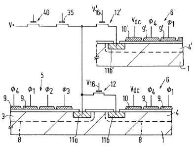
processing. Figure 10 is a sectional view of a variation of the first
embodiment, in which the potential of the zone 11 can be readjusted in a
different manner. For this purpose, the zone 11 is subdivided into two
spaced subzones 11a and 1lb, which constitute the output diode of the
channel 3 and the input diode of the channel 4, respectively. The zones
lla snd 1lb constitute (or are connected to) the source and drain zones
Q~ the switching MOST 12. This transistor can be simply for~ed by
providing on the oxide 19 between the subzones 11a, 11b the gate 16
indicated by broken lines. The output diode 11a is further connected to
one of the main electrode regions of the field effect transis~or 12 , of
which the other main electrode region is connected through the field
effect transistor 40 to a refexence voltage Vt. The parameters of the
transistor 40 are assumed to be identical to the parameters of the
transistor, whose source is constituted by the zone 11b, whose gate is
constituted by ~he electrode 10 and whose drain is cons~ituted by the
channel 4 below ~4. The voltage Vt can be chosen so that the
potential of the zone 11a is maintained at the threshold voltage 28 of
this transistor. During operation, in the case in which charge should he
transferred from the channel 3 to the channel 4, the transistor 12 is
closed, while the transistor 12 is open. In the case in which charge
packets have to be drained, the transistor 12 is opened and the
transistor 12 is closed. With a suitable choice of the voltage to be
applied to the gate of the transistor 40, i~Ç~ the same voltage Vdc as
that applied to the gate 10 and with the same threshold voltage below
the gate of the transistor 40 as below the gate 1~, the potential of the
zone 11a practically does not vary. As a result, the nextfollowing
signal which is supplied through the channel 3 after tha switch 12 has
been closed again and the switch 12 has been opened, can be transferred
without disturbance via the connection 11a, 12, 11b to the channel 4 and
can be transported further v a the channel 4 for further ~ignal
processing.
In an analogous manner, in the embodiment shown in Figure
8, the potential of the zone 11a can be adjusted to the desired values
by means of a similar transistor 40.
In the embodiments described here, it may oceur that
PHN 11.621 11 10.11.1986
fluctuations of the substra~e potential, for example due to clock cross-
talk, influence the signal transmission y~ the switchable connection
11, 12. Figure 9 shows diagramma~ically a method of reducing this cross-
talk. In the drawing, the input part of the ccd segment 6 (or of the
segment 6 ) is shown again. The d.c. electrode 10 is now not connected,
however, directly to the voltage Vdc, but is connected thereto through
an impedance Z. The gate 10 is coupled on the other hand to the
substrate 1 Ya~ a capacitor, which in the present embodiment is
constituted by a ~OS capacitor 36, which is provided in the
semiconductor body 1. The capacitor co~prises a ~-type sur~ace zone
37, which is provided at the surface 2 and constitutes one plate of the
capacitor 36, which is connected to the substrate 1 and an electrode 38
of metal or of polycrystalline silicon or another suitable conductive
material, which constitutes the other plate of the capacitor, which is
connected to the d.c. gate 10. The plates 37 and 38 are mutually
separated by a thin insulating layer 39, for example, an oxide layer,
which is formed simultaneously with the oxide layer below the clock
electrodes 9 and the d.c. gate 10. Potential fluctuations in the
substrate 1 are passed on via the capacitance 36 to the d.c. gate 10, as
a result of which the voltage between the d.c. gate 10 and the semi-
conductor body 1 is substantially insensitive to interference.
It will be appreciated that thq invention is not limited
to the embodiments described herein, but that ~any further variations
are possible for those skilled in the art without departing from the
scope of the invention.