Note: Descriptions are shown in the official language in which they were submitted.
.3~.
~MA/TDM INTERFACING
This invention relates ~o a communications system, and
interfaces therefor, in which a plurality of outstations
use a sinyle node as an intermediate for communicat~ons
wherein said communications ~nclude at least a proportlon
5 of digital traffic in time d~vision multiplexed form. The
network may use two channels, e.g. two radio channels,
both o~ which are used in a time-share mode.
The network comprising the outstations and the node
will be called herein a "time-division mult~ access",
conveniently abbreviated to ~DMA, system. The inventlon
particularly relates to an interface circuit for
interconnecting a TDMA system to an external station, i.e.
one which is not part of the TDMA system, which station
operates a plurality of channels in a time division
1~ multiplex farmat.
The inter~ace according to the invention is defined in
the claims.
The time division multiplex format commonly utilised
in UK takes the form of a frame which provides time-slots
~or 30 digital channels, i.e. 30 traffic slots. In
addition the ~rame has a slot, identified as "slot 0" for
synchronisation and a "slot 16", i.e. the seventeenth in
the sequence, whlch is used for signalling (that is
indicating the start and end of calls and identifying
numbers called to the exchange). Thus there axe 32 slots
in each frame.
It is also an accepted practice for a public "common
carrier" of telecommunications to connect suitable
customers to tile public switched network via a multiplexed
channel using the standard 32 slots even when ~he customer
does not need the 30 channels provided by 30 slots. In
those circumstances the operation is controlled so that
only assigned slots are used.
T~e interface according to the inventlon is capable of
operating with a wide range of external stations and, in
particular~ it is a~aptable to whatever proportion of the
multiplex frame is assigned to a par~icular external
5 station.
A preferred interface means provides three functions;
thus it comprises:-
(a) A first channel for accepting dig~tal ~ignals intime division multiplex format and provlding said
signals to a TDMA;
~bj A duplex channel for re-constituting signals
received via ~D~A into an assigned time divlsion
multiplex format; and
~c) T~lA circuitry for participating in the operation
of a ~DMA system, said TDMA circuitry being
operatively connected to items (a) and (b) above
to provide synchronisation and compatability
between the signals in said channels and the TDMA.
The first channel conveniently comprises gate-means
for selecting defined slots from received frames1 buffer
means for storing said selected slots and burst forming
means ~or concatenating TDMA information with the stored
slots to produce a burst. The gate-means preferably
comprises a frame-counter responsive to the sync slot in
~s each frame of a received multlplexed signal wherein said
frame-counter is operatively connected to a frame map
store and a buffer input gate and a channel map store in
such a manner that the frame-counter activates the buf~er
input gate to permit the passage o~ a byte when its count
matches a value retained in the channel map store.
The duplex channel conveniently includes a reception
buffer for storing received bursts, an output buffer for
storing regenerated frames and frame regeneration means
for transferring bytes from the reception buffer to the
output buffer and for incorporating blank slots in
accordance with synchronisation markers contained in said
received bursts to reconstitute the specified frames.
Preferably the duplex channel also includes a slot
control counter operatively linked to the channel map
store to control a frame gate to pass either bytes from
the reception bufer to the output buffer or to pass blank
slots to the output buffer and a synchronisation detector
or synchronising the count of the slot control counter
with synchronisation bytes provided by the reception
bufer wherein said synchronisation detector i5 responsive
to output of the frame gate.
The TDMA circuitry conforms to the re~uirements o
the TDMA system. In particular the interface circuitry of
this invention is compatible with the TDMA system
disclosed in our Canadian Patent ~pplication No. 4~2,307
filed August 31, 1984.
In this specification reerences to "our earlier
application" mean the application specified above.
Our earlier application is characterised in that the
communication, in both directions, takes the Eorm of a
sequence of traffic bursts wherein each traffic burst
includes a marl<er for synchronisation. It is a particular
feature that each active outstation utilises
synchronisation markers only in its own bursts. On
5 receipt of a burst an active outstation in~tiates a
pre-set delay and it returns a burst to the node. lhe
node has control of all the outstations and it adjusts
each pre-set delay so that bursts received at the node are
in the correct sequence.
1~ ~he outstat~ons require clocks which are used~ in
con~unction with the markers, to keep synchronisation. As
descrioed in our earlier application, the node has control
of the syncnronisation of the system because (a) all
clocks are derived From a master clock at the node, ~b)
the phasing o~ the clocks is fixed by synchronisation
markers transmitted by the node and (c) the pre-set delays
are ad~usted by the node.
~ he outstations o~ our earlier application are
synchronised to transmit ln turn. Since it is unwise to
rely on perfect adjustment the synchronisation is desi~ned
with gaps to reduce the occurrence of overlaps. There
will be large gaps when outstations do not wish to
transmit ~and there will be complete silence when no
outstation wishes to transmit). Thus the reception at the
n~de has a discon~inuous burst structure.
As our earlier applica~ion points out the information
bearing transmissions from the node have a similar
discontinuous burst structure but clocks dependant on the
node would cease to function during gaps and this could
30 have an adverse effect on system performance. It is,
therefore, desirable that the node generates a random~sed
pseudo-signal which is used to fill the gaps between
-- 5 --
in~nrmatiQn-contairling bursts. Thus the transmission from
t~le node has a discontinuous burst structure in respect of
the information bearing content but the discontinuities
are filled with timing signal whereby dependant clocks are
kept in adjustment.
S One embodiment of tlle invent~on will now be descrlbed
by way of exalnple with reference to the accompanying
drawings, in which:-
Figure 1 illustrates a radio network showing a node
and some outstatlons,
1~ Figure 2 is a diagram of an outstation,
Figure 3 is a diagram of the node, and
Figure 4 is a block diagram illustrating the ma~or
functions of the cards according to this invention and
included in Figures 2 and 3.
1~ ~he multipoint radio system illustrated in Figure 1
comprises a node which transmits to a plurality of
outstations on one frequency and receives from all the
outstations on a different frequency. Each outstation is
connected to, and provides service ~or one or more
~ customers. A commercial system could provide service for
up to 256 cust~ners distributed among 50-70 outstations;
these numbers could be reduced if one of the customers
provides a ~ery high traf~ic load. (A greater number of
outstations increases the cost thereof but decreases the
distances between the outstations and their customers so
reducing the costs of wiring. ~he optimum for any system
is a compromise based upon the geographic~l distribution
of the customers).
Figure 1 shows three of the outstations (11, 12 ? and
13) in communlcation with a node 10. The outstations
include interface circuits in the form of terminal cards
~ 3
-- 6 --
each of which handles the traffic for a single customer.
Outstation 11 has four terminal cards llA-llD; outst3tion
12 has six terminal cards 12A~12F and outstation 13 has
only one terminal card 13A. Clearly Figure 1 does not
S indicate the ~ull extent of a commmercial system but it
makes the point that there are a plurality of outstations
some, and perhaps all, of which serve a plurality of
terminal cards. The terminal cards provide ports for the
connection of external stations, eg stations ~hich are
operated by customers.
It is emphasised that different customers, requirlng
different services, would require di~ferent forms of
terminal card. This in~ention is specifically concerned
with the terminal cards w~lich provide an inter~ace for a
1~ PGM multiplex. Each such card provides an intarface for
one PCM multiplex; each multiplex nee~s its own card.
Other customers, e.g. single channel customers, would
require different cards. Any ~DMA system may include a
variety of different types of card. Thus the TDMA system
provides interchangeable access for customers with
different requirements because the different caxds convert
different external formats into a common TDMA format.
The system operates in frames of about lOms duration
and each frame consists of about 80ûO bytes of which about
~5 2000 are often required for sys~em ~nformation, i.e. GO00
are usually available for traffic. When transmitting, a
customer needs lOO bytes in each frame or up to 4000 bytes
in each frame for a customer with many au~io channels so
that a maximum of 60 customers could use the system
30 simultaneously. It is possible to connnect up to 256
small scale customers to the system which means that, at
most J only about 2û per cent of the customers can use the
_ 7 _ ~L~qi~
system at the san-le time. It therefore follows that idle
custolners cannot have access to traffic slots and a
customer has to be allocated to a traffic slot on changing
from an idle to an active state. If a large scale
customer is included in the system it is necessary to
5 reduce the number of small scale customers. It is also
possible ~or a priority customer to be given permanent
access to the TDMA system.
An arrangement, suitable at the outstations, will now
be described with reference to Fiyure ~.
It T~e outstation comprises an antenna ~0 which is used
in both send and receive modes. In the receive mode the
antenna 40 picks up signals ~rom the node and passes them
to receiver 42 via coupler 41. Receiver 42 performs all
the usual receiver functions and it passes the demodulated
and regenerated traffic to con~mon ~nterface l~7 via line
46. Receiver 42 also recovers a clock from the incoming
signal and the clock passes, on line 45, to inter~ace 47.
In the send ~ode transmitter 44 is connected to
antenna 40 vla burst switch 43 and coupler 41. ~he
transmitter obtains its data ~rom interface 47 via line
51. Burst switch 43 is controlled from the interface via
line 48. The burst switch 43 is normally open and in this
orientation the signal from the transmitter does not reach
the antenna 40. When closed, burst switch 43 allows the
signal to reach the antenna 40 whence it is radiated to
the node~
Interface 47 is adapted to contain ter~inal cards 50A
to 50E each of which, as mentioned above, handles the
traffic ~or one customer. Because the terminal cards
3~ 50A-5aE are connected to interface 47 each receives all
the signal and a clock. Each can provide traffic for
transmission and control burst switch 43.
8 -
~Card 50~, as well as serving its customer, also acts
as an outstation card to provide radio information to the
node and to receive control signals for any radio
functions controlled ~rom the node).
The identity o~ each card is (adjustably3 hard wired
as part of interface 47. Thus in case of a fault, an old
card can be removed and a new card inserted.
Each te~ninal card 50 is connected to its custo~er's
equipment but these connections are not shown in figure ~.
1~ As shown in ~igure 3, the node comprises an antelma 60
which is used in both send and receive modes. In the
receive mode it picks up signals from all the outstations
and passes them to receiver 62 which demodulates and
regenerates the data which is passed to the common
interface 64 on line 70. The receiver 62 also derives a
clock from the received signal and this derived clock is
passed to interface 64 on line 71.
~raffic for transmission passes from the interface 64
to t~ans~itter 63 and then to antenna 60.
~ Since the node handles traffic for all the customers
it includes terminal cards 66 and it requires a card for
each active channel. It also includes a system card 65
for timeslot zero and a generator 67 ~or pseudo-random
signals to ~111 in any gaps in transmission.
~5 The node also includes master clock 69 and
microprocessor 68,
In addition, the termina~ cards 66 are connected to a
teleco~munications network so that traffic received by the
cards 66 can be passed on to the destination. I~ two
customers o~ the system wish to communicate with ona
another their cards are interconnected via the
telecommunications network.
_ 9 _ 3LA~
All slgnals related to system information are handled
via the microprocessor 68. It should be noted that the
microprocessor 68 has direct control of system card 65 and
all t~e terminal cards 66. Microprocessor 68 also has
control~ via system card 65 and the radio, of all the idle
cards (i.e. cards in t~le outstations synchronised to
system card 6S at tl~e node~ at all the outstations.
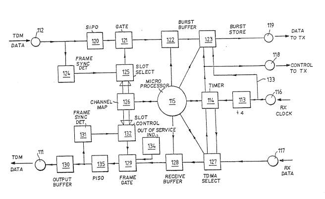
An interface circuit adapted to co-opera~e with the
transmitter and receiver of an outstation as shGwn in
Figure 2`and a node as shown in Fiyure 3 is illustrated in
Figure 4. The interface circuit corresponds to car~s 50
of Figure 2 and cards 66 of Figure 3.
The interface circuit has two ports, 111 and 11~,
which provide connections to the private exchange of a
customer) sai~ exchange using a time division multiplex
operational node which will be described below. The card
also has four ports, llS, 117, 118 and 119, which provide
connections to the transmitter and receiver of the
outstatioll. More specifically the ports perform the
following functions:-
PORT 112 receives traffic, in multiplex form, from
the customer's exchange;
RT_lll outputs traffic, ln multiplex form, to the
customer's exchange;
~5 Rt 116 receives clock signals from the receiver of
the outstation;
PURT 117 receives traffic from the receiver of the
-
outstation;
RT 118 sends control signals to the transmitter of
the outstation;
RT 119 sends traffic to the transmitter of the
outstation.
-- 10 -
Before describing the functions of the card the ~o~mat
of the multiplex will be defined.
~ he multiplex takes the form of a ~rame which contains
32 slots each adapated to contain a byte, i.e. the eight
bits which specify the value of a speech sample. In
accordance with conventional practice the multiplex frame
lasts for 1~5 ?s. Out of each frame one slot, i.e. "slot
O" contains a synchronisation marker which enables
exchanges and demultiplexers to synchronise~ In addition
lo slot 15 contains signal information which is needed by the
exchan~es. (It should be understood that this is a
conventional ,~rame in telecommunications. The invention
~ill also function with other frame formats.)
The format ~ust identi~ied provides for thirty
15 speech/data channels; in public switched networks it is
used for this purpose. However a customer may only want
to use a smaller number of lines, e.g. ~ive. If the
customer is using a private exchange which employs time
division multiplex, it is convenient to retain this mode
for communication to the public switched network. This is
achieved by providin~ a channel using the conventional 32
slots~per-frame but only utilising 5 of the slots for
tra~fic The ~ive ~lots can be located anywhere within
the ~rame, e.g. slots 3, 11, 13, 19 and 25 could be used
~5 (although it might be more convenient to use ad~acent
slots, e.g. 7 to 11). In any case slo~s O and 16 would be
included to provide sync and signalling in~ormation
(making seven slots in total). ~he unused slots (25 in
number) are filled with "out-o~-use" markers to ~acilitate
processing.
It will be appreciated that the multiplex format
described above actively limits each customer to a
specified number of slots. If the custorners were allowed
to exceed this limit public service exchanges could be
overloaded and~or other custsorllers could be unfairly
affected. If the link between the customer and the
exohange is provided by a time division multi-access
systern it is necessary to convert the continuous multiplex
system described above to the t~urst-mode of the TDMA. The
inter~ace device promotes this conversion. The TDMA has a
cycle time of 10 ms. Since each multiplex frame last for
1~ 125 ~s thls means that each TDMA cycle must carry 80
multiplex frames. For a total of seven slots per frame
the customer needs 560 bytes in each TDMA cycle.
As stated above the device includes port 112 adapted
for connection to a customer s exchange to receive
multiplexed signals in the format described above. The
port 112 is connected to bit serial~bit parallel converter
l~û wlllch is connected to burst store 1~ via gate 121 and
burst-t~uffer 122. The output of burst s~ore 123 is
connected to burst output port llg. ~rame sync detector
124 and slot selector 125 are connected in parallel with
the converter 120. The ouput of slot selector 125 is
connected as the control of gate 1210 Slot selector 125
is connected to channel map 126 which stores
identifications cf ttle multiplex slots in use; for the
2tj example given above channel map 126 stores representations
of the integers 0 3 11 13 1~ 19 and ~S.
The interFace also includes a duplex channel for
receiving traffic from the TDMA system and providing it to
the customer s exchange. This channel cornprises TDMA
selection means 127 having its input connected to port 117
and its output connected to reception buffer 128. PGM
output port 111 is connected to receive output from output
~ 3
- 12 -
buffer 130 which receives i~s input through
parallel/serial converters 135 from either out-of-service
indicator 134 or from reception buffer 128 in accordance
with the setting of frame-gate 129. Frame gate 129 is
5 controlled by slot control 132 which is connected to
channel map 126.
The interface also contains items to perform TDM~
functions tas described in our aEoresaid Canadian Patent
Application No. 462,307 filed August 31~ 1984)o These
lt~ms are port 116 for receiving a clock signal from the
receiver oE the outstation. Since the frequency of this
slot signal is inconveniently high for internal functions
port 116 is connected to divider 113 which divides the
frequellcy by four. Port llS is also connected, via clock-
line 133, to burst store 123 so that this store receives
unmodified TD~ clock. The timer 114 operates on a cycle
equal to the period of the TDMA and the zero oE the cycle
is ad]usted to correspond to the reception of each burst
intended for the interface device. The timer 114 is
connected to the burst store 123, microprocessor 115,
selection means 127 (as described in our aforesaid
Canadian Patent application No. 462,307).
The operation of the device will now be described;
the ~escription will concentrate on the compatibility with
~5 PCM-multiplex. Description of TDMA functions will be
minimised since the preferred TDMA is described in our
earlier cases.
PCM signals are accepted at input port 112 and
converted into bit-parallel form in converter 120. Frame
sync (i.e. the bit sequence in slot 0) is detected in
detector 124 which provides a sync signal to lot selector
125 at the start of each multiplex frame. Thus the
selector 125 is enabled to count the slots whereby the
count in selector 125 corresponds to the slot in converter
a~
- 13 -
120. Slot selector 12S is connected to channel map 126
which contains data representations deflning the
meaningful slots of the multiplex frame. When the count
current in selector 125 matches any one of the "mapped"
slots stored in challllel map 126, selector 125 actuates
gate 121 with the result that the byte in converter 120 ls
transferred to storage in input buffer 122. Thus bu~fer
122 accumulates all the meaningful slots over a number of
frames.
Io It is emphasised that the synchronisation slots are
selected by selector 125 and buffer 122 preserves
chronol~gical sequence. Thus the original multiplex frame
structure is inherent in the stored data representations;
no ad~itlonal multiplex synchronisation is provided (and
none is necessary).
The input to buffer 123 operates in synchronisation
with, and indeed as part of, the input time div~sion
multiplex system. The output of buffer 123, which
operates as part of the TDMA system, will now be described.
~0 Tne microprocessor 115, once in each TDM~ cycle,
activates burst-buffer 122 to transfer all its content to
burst store 123. The microprocessor 115 is operatively
connected to timer 114 which is synchronised to the TDMA
cycle so that this trans~er is made ~ust before a burst is
~5 due for transmission.
As mentioned above the ~DMA cycle has a duration equal
to 80 multiplex frames. Thus the transfer occurs one for
every ~0 multiplex frames. Each multiplex `frame contains
one slot for each speech channel plus one slot for sync
30 (i.e. slot 0) and one slot for signalling (slot 16). In
the example given above five speech channels were assumed
to be utilised and this gives seven bytes per multiplex
~ 14 -
frame so that 560 bytes are ~ransferred at each cycle.
Whilst it is important that the (PCM frame):(TDMA cycle)
ratio be kept at 80:1 there ~s no need for explicit
synchronisation between the multiplex and the TDM~.
After transfer of the 480 bytes to the burst store
the microprocessor adds the bytes needed to operate the
~DMA; for example the microprocessor may add a preamble
consisting of three bytes to enable the receiver to
establish bit-synchronisation t~lree bytes for burst
1~ identification and one byte each for system identification
and customer address. In addition eight bytes (makin~
sixteen) are reserved by microprocessor llS for ~MA
information and a further ten bytes (making twenty six in
~11) are left empty to serve as "guard time" to protect
l~ against imper~ections of ~DMA sync. Thus the 560 bytes
(transferred from burst buffer 122) are augmented to 586
bytes which constitutes the burst which is stored in burst
store 123 until burst transmission time.
The actual tr~nsmission is performed under the control
of timer 114 and the clock signal on line 133. The timer
by virtue of its synchronisation to the cycle of the TDMQ
determines t~ `'wiodow`' during which the burst is
transmltted. During the "windo~" the timer 114 provides
enable signals to burst store 123 and control port 118.
~hen located in an outstation or a node the enable
signal on control port llB passes to the transmitter
causin~ it to adopt the "send" mode ~or the transmission
o~ the burst. The enable signal to burst store 123 causes
it to pass its contents9 in bit-serial form to traffic
output port 119 at a bit rate con~rolled by the clock
signal received at clock port 116. From port 119 the
signal passes to the modulator of the outstation's
- 15 -
transmitter whereby said siynal is transmitted to the
node. lt is empl)asised that the clock signal from port
116, and hence timer 114, is provided by the TDMQ system
so that the burst is transmitted at tha correct time and
at the correct bit rate.
lt will be appreciated that the channel ~ust described
enables the interface circuit to accept signals in the
form of a PCM time multlplex, to remove unused slots from
these signals and tc provide t~e signals as a burst for
ll~ the ~D~IA The interface includes a duplex channel which
reverses this process. ~his duplex channel will now be
described.
The duplex c~annel receives its trafflc from input
port 117. During use all the traf~ic is passed to
1~ selection means 127 whicll is normally in a "disabled"
state. For a sllort period (ad~acent to the zero of cyclic
timer 114) the selection means 127 is enabled by the timer
114~ During this period selection means 127 is responsive
to the ~DMA synchronisation pattern and to its own address
~0 so that it recognises its own incoming burst. On
recognition it initiates data capture and it remains
enabled until data capture is complete. Durin~ data
captuxe it converts the bit-serial input into bit-parallel
~orm and it accepts a fixed number of bytes for storage in
~5 reception buffer 128. (Above it was stated that the burst
wa~ sao bytes long when it was transmitted, therefore the
"fixed number" is 580. If desired a mar~in for error may
be provided by using a higher fixed number e.g. 60U.)
When data capture is complete the fixed number of
bytes is stoxed in reception buffer 128 and means 127
returns to its "disabled" state. In the next par~ of the
reception cycle microprocessor llS checks the contents of
36
~ 16 -
reception buffer 12~. This check comprises verification
of the lDMA information whereby correct TDMA performance
is checked. This verification lncludes a check upon, and
if necessary correction of, the phase of timer 114. When
the 7DMA verification is complete the microprocessor 115
deletes tlle ~DM~-related bytes (and any excess bytes
acquired as a mar~in for error) to leave the traffic bytes
which, in correct operation, will be identical to the
transrnitted bytes.
If deslred tlle microprocessor may check the remaining
bytes, iOe. the traffic bytes, to conform that "slot 0"
occurs regularly and at the correct intervals. This will
also identify the first slot in the sequence.
Microprocessor 115 stores the identity of the last byte of
the previous burst so that it can confirm that the correct
sequence is malntained.
(Note. The transmissiorl process arbitrarily chops the
contirluous flow of traffic bytes into bursts but the
sequence ls maintained because the last byte of each burst
is followed, about 10 ms later, by the first byte of the
next burst. The reception process is about to
re-establish the continuous flow and the microprocessor
115 has just conFirme~ that the intended operation is in
fact happening. It is, there~ore, able to detect
malfurlctions. If the microprocessor 115 detects frequent
errors this suggests system-failure and microprocessor 11
issues an alarm to the engineers.)
When microprocessor 115 has completed all its checks
the contents of reception buffer 128 are transferred to
multiplex output buffer 130 via fra~e ga~e 129 under
control of slot control 132 which keeps a count de~ining
the slot position in the output frarne. When the count
, :,
- 17 -
current in slot control 132 matches any one of the
"mapped" slots stored in channel map 126 slot control 132
actuates frame gate 129 to select a byte from buffer 128.
In all other cases frame gate 129 selects a byte from out
5 of service indicator 134. Thus selected byte passes to
output buffer 130 via parallel/bit serial convertor 135.
The output of frame-gate 129 is checked by frame-sync
~etector 131 whlcl- detects "slot 0" and provides a sync
signal to slot control 132. Th~s has the effect that the
count in slot cor)trol 132 is adjusted so that the "zero
count" occurs when bytes equivalent to slot 0 are
transferred from reception bu~fer 128. Thus the correct
frame format is established in output buffex 13û~
Output buffer 130 provides its output in bit-serial
form at the rate of the PCM multiplex to PCM output port
111. Thus the required multiplex forrnat is provided as
output after passage througl- a ~DMA system.
It is emphasised that the TDMA operates as described
in our ea~lier patent application and customers can be
~ allocated burst time as needed. Modificat~on of the TDMA
pattern may also be appropriate in certain circumstances
e.g. a customer with many channels may be allowed
permanent access to the TDMA The unallocated capacity
could be shared between customers as described in our
~5 earller applications
The embodiment described above utilises an
unel-angeable channel map and a fixed burst length; i.e.
the customer has a fixed allocation of channels. There
can be a gain of flexibility by modifying the system to
permit ad~ustment o~ the number o~ channels (subject to a
specified maximum) as needed. In order to make this
adjustment possible it is necessary to provide the
3~
- 18 -
customer's PABX with means to communicate with the TDMA,
e.g. by arranging that the microprocessor 115 has access
to slot 16 of the multiplex frame. This enables the
microprocessor 115 to request a new burst length over the
signal system of the TDMA and to reset channel map 126.
lhus the interface described above makes possible
direct connection of multiplexed audio channels using PCM
to a ~digital) time divislon access system. Furthermore~
in the case of multiplexes having a suff~cient proportion
l~ of acti~e slots in the frame, the multiplex uses a shorter
burst length than the same number of separate audio
channels. In ~his aspect the break even po~nt occurs at 7
channels in a multiplex with 32 frames there being two
system slots, i.e. slot 0 for sync and slot 16 ~or
signalling. Thus a simple audio channel requires 80 bytes
for audio plus 26 bytes for ~DMA purposes~ i.e. 106 bytes
per frame. Thus 7 such channels require 74~ bytes. The
e~uivalent multiplex requires 7 slots for audio plus 2
slots for system which makes 720 bytes for the 80 frames
~) in each burst. The burst also requires 26 bytes giving
746 bytes in all this is substantially the same time
demand for both techniques. The multiplex only re~uires 1
interface card whereas seven separate channels require 7
cards. If the traffic is provided as a multiplex, the
~5 multiplex card of the invention is compatible wereas extra
interface equipment would be needed to separate the
separate audio channels. (1~ it were of oYerwhelming
importance to provide maximum flexibility in the handling
of the seven audio channels then separate handling might
be preferred.)
Where less than seven channels are used the separate
channels give a shorter total burst ti~e than the
multiplex but, if the traffic were required as a multiplex
then the invention provides compatibility.