Note: Descriptions are shown in the official language in which they were submitted.
6~
MICI~(~COMPUTE~ cONrLl~0~ QUICK RANGII`~JG
TECtlNlQUE AND l~ AL FIL~R
BACKGROUND ANO SUMMARY OF THE INYENTION
._ I
This invention relates generally to the field of electronically controlled
compasses for use in an automobile. More specifically, it relates to the type of
electronic compass which employs a flux-gate sensor similar to the type described in the
article by Garner entitled "A Magnetic Heading Reference For The Electro Fluidic Auto,
Pilot" which appeared in two parts, one in the November 1981, and one in the December
19~1 issues of Sport Aviation ~
.'
The theory on operation of flux-gate magnetic field sensors in an automotive
application is further described in an article entitled "Magnetic Field Sensor And Its
Application To Automobiles" by Hisatsugu Itoh dated February, 1980 and published by the
Society of Automotive Engineers as "Paper No. 800123.".
. ,,1
Further examples of work in the area of electronic compasses appears in thel,
following U.S~ patents: 3,943,763 issued March 16, 1976 to Howell D. Garner entitled
"Magnetic Heading Reference"; 4,424,631 issued ~anuary 10, 1984 to Franks entitled
"Electrical Compass"; 4,425,717 issued January 17, 1984 to Marcus entitled "Vehicle
Magnetic Sensor"; 4,505,054 issued March 19, 1985 to Clark et al. entitled "Magnetic
Sensor Mounting System"; and 4,546,551 issued October 15, 1985 to Franks entitled
"Electrical Control System." I
The 3,943,763 patent to Garner describes an electrically cornpensated,
magnetometer (A magnetometer's function is to detect magnetic fields and to measurel
their magnitude and direction.) It provides a means for cornpensating for the northerly,
turning error in a magnetometer used as a heading reference for a vehicle such as an
aircraft. Northerly turning error is described in "A Magnetic Heading Reference For the
Electro Fluidic Auto Pilot"~ the articles cited above. Basically it arises from the fact
-1-
,r.. .! .
that the earth's magnetic field is no~ horizontal except for a few locations. The lines of
magnetic flux in the United States are between 60 to 75 degrees from the horizontal.
This, according to Garner's Sport Aviation articles, is the dip angle.
The 4,424,631 patent to Franks describes a circuit to work with an electrical
compass. It features an oscillator coupled to a digital bandpass filter and a synchronous
phase detector in such a way that the frequency and phase of output signals from a flux-
gate sensor have a predetermined relationship to the excitation signal. According to
Franks, this results in a tuning free design since ~he same oscillator signal is presented to
excite the flux-gate sensor.
The 4,425,717 patent to Marcus describes a flux-gate sensor mounting
structure for an electrical compass in a vehicle. According to Marcus, the loca~ion of
the sensor in association with the rearview mirror somewhat isolates the sensor from the
metallic mass of the vehicle and from the vehicle's wiring.
The 4,505,054 patent to Clark et al. describes another mounting system for a
flux-gate sensor. According to Clark et al., this mounting structure includes a cradle for
pivotally mounting the sensor for adjustable movement in a vertical plane aligned with
the longitudinal axis of a vehicle.
The 4,546,551 patent also to Franks describes an electrical control system,
including a microcomputer for correction control of an electrical compass. The
correction signal is applied directly to the sensor windings to drive the sensor output~
signal to the desired level. Northerly turning error is corrected via a signal processing
procedure which affects the display output signals based on stored variation correction
angle information.
An object of the present invention is to improve the systems of the prior art
by supplying a simplified calibration technique utilizing the combination of software and
-2-
~ '
.
7 ~
hardware; the hardware being used to operate with voltage
levels in required ranges and the software used to perform
the precise calibration.
Specifically, the invention relates to a quick
ranging technique for each magnetic component for use in a
calibration technique, with stored charge times, for an
electronic compass control circuit that includes a
microcomputer, a flux-gate, a flux-gate driver, a bandpass
filter, a synchronous detector, an integrator, and a summing
1~ amplifier; the control circuit equipped with a ranging
circuit that includes: an operational amplifier with
resistive negative feedback connected to the output of the
integrator; an RC charging network connected to the non-
inverting input to the operational amplifier; a gate switch
connected between the RC charging network and the
microcomputer such that the microcomputer charges the RC
charging network when the gate switch is closed; and
comparator means to respond to the output of the integrator
to control the operation of the gate switch. The quick
~0 ranging technique comprises: using the stored charge time
associated with the magnetic component being measured to
charge the RC charging network; monitoring the integrator
output to see whether the voltage is within the calibration
range; adjusting the charge time with a delta charge time
from a ranging table if the voltage is not within range until
the voltage is within range; storing the adjusted charge time
rn/
~ ~r ~
;~t~6,~7~
3 a
as t~e new charge time associated wi-th -the magne-tic
components to be used each time that componen-t is measured b~
charging the RC charging network for the stored charye time.
In another aspect, the invention relates to a
digital filtering technique to smooth out the magnetic field
component signals for an electronic compass control circuit
that includes a microcomputer, a flux-gate, a flu~-gate
driver, a bandpass filter, a synchronous detector, an
integrator, and a summing ampllfier; the control circuit
equipped with a ranging circuit that includes: an operational
amplifier with resistive negative feedback connected to the
output of the integrator; an RC charging network connected to
the non-inverting input to the operational amplifier; a gate
switch connected between the RC charging network and the
microcomputer such that the microcomputer charged the RC
charging network when the gate switch is closed; and
comparator means to respond to the output of the integrator
to control the operation of the gate switch. The technique
comprises: redefining the filtered value to be the most
2~ recent unfiltered value divided by three plus the most recent
~iltered value multiplied by two-thirds; using the new
filtered values when computing the compass headiny.
Related subject matter is disclosed in applicant's
copending Canadian applications serial nos. 516,815 and
516,816, both filed on August 26, 1986.
rn/~
DESCRIPTION OF TH~ DRAWINGS
Other objects, features and advantages of the present invention will become~
more fully apparent from the following detailed description of the preferred ¦
embodiment, the appended claims and in the accompanying drawings in which:
Fig. 1 is a block diagram of the electronic compass control hardware;
Fi8. 2a is a schematic diagram of the electronic compass circuitry;
Fig. 2b is the continued schematic diagram of the electronic compass
circuitry;
Fig. 3 is a flowchart for the compass calibration;
Fig. 4 is a flowchart for setting the compass variance;
Fig. 5a is the flowchart of the calibration/ranging procedure;
Fig. 5b is a continuated flowchart of the calibration/ranging procedure;
Fig. 6 is the flowchart of the auto-ranging procedure;
Fig. 7 is a timing diagram illustrating the signals at the integrator output,
ranging circuit, ranging control pin and multiplex circuit;
Fig. ~ is a timing diagram of the synchronous detector signal and the coil
driver signal;
Fig. 9 is a flowchart of the reading and filtering of the magnetic field
components; and
Fig. 10 is a graph showing the feedback for quick ranging.
. I
~ 7~
DETAII,~D DESCRiPTlON OF_THE PREFEf~F~ED EMBODIMENT
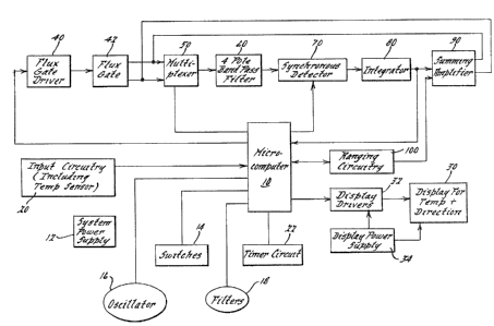
Referring to Fig. 1~ illustrated is a block diagram of the electronic compass.
The heart of the system is a microcomputer 10 which interfaces with almost every other
cornponent shown in the diagram. The microcomputer 10 receives its power through
power supply 12 as does many of the other components on the figure. Therefore, the
power supply 12 is not connected to any of the diagrams at any of the components on~
Fi~. 1 to keep the diagram less cluttered.
Switches 14 are provided to work with the microcomputer and allow the
operator of an automotive vehicle equipped with an electronic compass to communicate~
with the microcomputer 10. Oscillator 16 generates a signal which the microcomputer
10 uses for timing and for signal processing. Capacitors 18 are used as resets and filters
throughout the circuit and are diagrammatically shown as being connected to
microcomputer 10. Their function is to dampen out noise and to provide some signall
conditioning where necessary. The switches 14 function to allow the driver to calibrate¦
the system, make manual inputs for the directional variations, engage or disengage a¦
temperature reading, engage or disengage the compass and/or to display the results in
U.S. or metric units~
The input circuitry 20 is in communication with the microcomputer 10 and
consists of components to control the intensity of the display 30 and also the reading of
the thermister type temperature sensor.
,,
The timer circuit 22 exists to account for the possibility that the vehicle will¦
be restarted before the temperature of the engine drops to the ambient temperature
period. Under that circumstance, without the timer, the thermister temperature sensor
would sense a higher ambient temperature due to the temperature radiating from ~he
engine instead of the actual ambient temperature. The one hour timer 22 retains the
last-sensed ambient temperature to allow the engine to return to ambient tempe~ature.
The specification on the one hour timer is plus or minus 15 minutes.
7~L
The display 30 is controlled by the micro-
computer 10 an~ provides a visual readout of the output
gellerated by the electronic compass circuit and tha-t
generated by the -temperature sensor shown in F:ig. 1.
This display ls then read by the opera-tor of the auto-
mobile to show him or her the direetion the vehicle is
traveling in. The display 30 is driven by display
drivers 32 and the display power supply 34. The display
power supply 34 uses transformers made specifically for
this application. Many of the components are s-tandard
off-the-shelf integrated circuits and power supply
chips. The display power supply 34 acts as a constant
frequency switching regulator.
The microcomputer 10 also works in conjunction
with a flux-gate driver 40 and flux-gate 42. The flux-
gate operation can best be described in referring to the
document entitled "A Magnetic Heading Reference For The
Electro Fluidic Auto Pilot" referred -to in the Background
and Summary of the Invention.
The flux-gate driver 40 takes a square wave
signal from the microprocessor or microeomputer 10 and
adds enough drive to it to saturate the flux-gate 42.
This operation is again explained in "A Magnetie Heading
Referenee For The Eleetro Fluidic Auto Pilot" and
"Magnetie Field Sensor And Its Applieation To Automobiles
(SAE Paper No. 800123)".
The flux-gate eommunieates with multiplexer 50.
The multiplexer 50 is also in eommunieation with miero-
eomputer 10. The multiplexer 50 is in eommunieation with
a four pole bandpass filter 60 whieh feeds the filtered
signal to a synchronous deteetor 70.
Feedback from the synchronous detector 70 works
to stabilize the entire compass control system shown in
Fig. 1 by feeding back a portion of its current through
integrator 80 and summing amplifier 90 to the flux-gate
42. The fed back eurrent eventually beeomes an equal
and opposite signal versus that produeed by the flux-ga-te
42 as the flux-gate 42 senses the magnetie field.
s ~
More specifically, the output of the bandpass filter 60, which is ed into the
gate switch 102C (shown in Fig. 2a) and then ~o the integrator 80, is a sinusoidal signal.
The sinusoid is fed into the gate switch 102C which is pulsed on and off at the
same frequency controlled by the microcomputer 10. The resultant output of the gate
switch sensor is a half wave rectified signal fed into the inte~rator 80.
The output of the integrator 80 is a D.C. Ievel. When the sensed magnetic
field of the earth produces a signal at the flux-gate 42, it is filtered through the
bandpass filter 60 and synchronous detector 70. Thus, it is positive half wave rectified
after exiting the gate-switch 102C. The output of the integrator 80 will gravitate
downward to balance the inputs on 103C. This output is fed back through the summing
amplifier 90 to the flux-gate 42 to adjust the current to the coils up or down and,
therefore, the signal presented to the bandpass 60 filter which stabilizes the D~C. Ievel
and the output of the integrator 80.
Likewise, if the input to the integrator 80 is a negative half wave rectified
signal from the bandpass filter 60 and gate-switch 102C, the output of the integrator 80
will rise to equalize the inputs. This raised output will be fed back to the flux-gate coils
in 42 through the summing amplifier 90 thereby adjusting the signal presented to the
bandpass filter 60, likewise preserving the stability of the system.
1,
To further amplify the description of the flux-gate 42, it should be
understood that the desire is to measure the earth's magnetic field which is a difficult
thing to accomplish. Therefore, the desire is to merely sense the signal produced in a
coil by the earth's magnetic field and to produce an equal and opposite ima8e of that
sensed signal in the same coil by a D.C. current.
In other words, when the north-sauth gate switch is closed, the signal
produced by the north-south component of the earth's magnetic field in the flux-gate coil
is balanced with the current generated in the feedback path. Likewise, when the east-
_7_
I
66~7~
west gate switch is closed, the signal produced by ~he east-west cornponent of the earth's;
magnetic field in the flux-~ate coil is balanced wi~h the current generated in the
feedback path from the summlng amplifier through resistor 149.
The current produced in the feedback path and fed through resistors 149 and
¦ 148 opposes the current generated in the coils as produced by the earth's magnetic field.
I !
I The second order harmonic signal from the four pole bandpass filter 60 i5
¦~ presented to the synchronous detector 70. The function of the synchronous detector 70
is to select the portion of the second harmonic to be integrated by integrator 80. The
output of the integrator 80 is a DC signal which is fed back through a summing amplifier;
90 to the secondary coil of flux-gate 42 at pins 3, 4, 5 and 6. This has the effect of,
cancelling out the input to the four pole bandpass filter. This provides stability to the j
system. I
The summing amplifier 90 also compares the output of ranging circuit 100 to,
that of the integrator 80. The signal is fed back to the input of the multiplexer 50 to
stabilize the systemO The stabilization effect is applied to both of the flux-gate sensor 1
outputs.
The ranging circuitry 100 interfaces with the microcomputer 10 in a way
which will be described below.
Referring now to Fig. 2a and Fig. 2b, the details of the circuit described in
the block diagram of Fig. 1 are provided.
Microcomputer 10 is an off-the-shelf commercially available microprocessor
with the Commercial Part Number MC6805S2.
The VCC power supply 12 provides power to the various components I
throughout the Fig. 2a and Fig. 2b. The Vcc power supply 12 supplies 5 and 10 volts to
-8 -
L7~L
the res~ of the system described and as shown in Fig. 2a and Fig. 2b. The heart o~ the
five-volt section of the Vcc power supply is a regulator chip U-200 which accepts an
input voltage from the battery through ~liode D-203 and coupled to logical ground to
capacitor C-200 into pin 1 of U 200. AISOJ aS an input to regulator U 2UO is the ignition
voltage IGNl presented to the switch-reset pin 4 of regulator 200 through diode D-202
and resistor R-201. Voltage VJ2 is available as the protected switched battery voltage
between diode D-202 and resistor R-201.
The regulator U-200 is provided with a heat sink M-200. The regulator U-200
is grounded through pin 3 to logic ground. The output of regulator U-200 comes from pin
2 and is partially maintained by capacitor C-201. For this particular application, the
output on pin 2 of regulator U-200 is five volts at approximately 750 milliamps. Also
available from regulator 200 is a stand-by five volt output voltage offered at pin ~ and
coupled to logical ground wi$h capacitor C_202. The stand-by five volt output is
available at 10 milliamps.
Also provided in the Vcc power supply is a ten volt section with an output of
voltage VA from transistor Q-200. Diodes D-200 and D-201, along with resistor 202 and
capacitors C-20~ and C-10~ work with transistor Q-200 to generate this ten volt output
as shown in the schematic.
Also available is another voltage taken from the ignition voltage and divided
down through resistor divider network R-211 and R-210 and supported by capacitor C-
210. The purpose of this circuit is to indirectly measure the ignition voltage in the
control dimming of the displays. This is an indirect measure of the ratio of display panel
voltage changes. The ignition voltage is measured indirectly across resistor R-210. The
ratio of the voltage across resistor R-210 to the voltage across the series connected
resistors R-211 and R-210 remains the same. Therefore, ignition voltage can always be
computed in microcomputer 10 by monitoring the voltage across R-210 and using it to
compute the ignition voltage in the ratiometric relationship stored in microcomputer 10.
7~
il
The ignition voltage is then used to coordinate the dimming of the display 30
after taking note of the signal presented to the A/D converter on pin 7 of microcornputer
10. This signal is generated by the operator turning the potentiometer switch connected
at DIM 3 as modified by resistor divider R117 and R116 and suppor~ed by capacitor C115.
The microcomputer adjusts tlle dimming signal given to the display clriver 32 as a
function of the indirectly measured ignition voltage presented to pin 9 of microcomputer
l 10.
Also providing inputs to the system shown in Fig. 2a and Fig. 2b is the
switching section 14. The switching section 14 comprises switching elements M221 -
M225, all of the switches operate in the same fashion, being connected between logic
ground and a pull-up resistor connected to Vcc. Some of the switches are double pole.
Vcc is connected to each of resistors R-120, R-121, R-122 and R-123 which, in turn, are
connected to the various switches M-221 through M-225. The junction between the
switches and the resistors are fed to various pins on the microcomputer 10 and the
microcomputer 10 senses when these points are tied to logic ground by means of an
operator action to close any of the switches M-221 through M-2~5. The switches allow~
the vehicle's operator to select a temperature function on M-221, a variance function on
switch 225, a U.S.-metric function on M-222, a calibration function on switch 224, and a
compensation function on switch M-223.
Oscillator section 16 provides crystal oscillator M-120 and capacitors C-120
and C-121 and presents a oscillator signal to the clock inputs of the microcomputer 10.
ll
Filter section 18 comprising reset capacitor C-122 connected to pin 23 f
microcomputer 10 and filter capacitor C-125 connected between tied pins 5,24 and tied
pins 1,6,28 are provided for resetting and filtering purposes.
The input circuitry section 20 presents inputs to pins 8, 7 and 22 of
microcomputer 10. When Mark-4 is high, dimming takes place according to dim voltage
and ignition voltage read as described on page 9. Mark-4 is high when lights are high
(unless overridden by detents).
-10-
.
l l
1266~ i
The input circuitry 20 consists of several components which control the
intensity of the display 30 and also the reading of a thermister-type temperature
transducer (not shown), but connected to Temp Sensor 2 through to pin 8 of
microcomputer lOo
Timer circuitry 22 presents a signal to pin 16 of the microcomputer 10 which
is 1 bit of an input port of microcomputer 10. The timer 22 exis~s to account for the
possibility that the vehicle will be restarted before the engine temperature drops to the
ambient temperature. Under that circumstance, without the timer, the thermister
temperature sensor would sense a higher ambient temperature due to the temperature
radiating from the engine instead of the actual ambient temperature. The one-hour
timer signals the software in microcomputer 10 to retain the last sensed ambient
temperature until the sensor returns to ambient temperature. The specification on the
timer i~ on hour +/- 15 minutes. The timer is of conventional design and consists of a
power operational amplifier V-lOla. Voltage VA from power supply 12 is presented to
the non-inverting input of U-lOla through a parallel circuit made up of resistor 151 as
one branch and parallel with diode 150 in series with resistor 152 in the other branch.
Also connected to the non-inverting input of view U-lOla is capacitor C-150 which is~
connected between the non-inverting input of U-lOla and ground. On the inverting input
to U-lOla, a resistor divider network made up of resistor R-154 and resistor R-153 isl
connected between the output of U-lOla and ground. The resistor divider point betweenl
R-153 and R-154 is connected to the inverting input which, in turn, is connected to pin
16 of the microcomputer 10.
I ,
The display section 30 is made up of a vacuum fluorescent display M-280.
VFIL+ and VFIL are supplied by power supply 12. The filament becomes red hot when so
supplied with voltage. The excitation of the filament causes electrons to be boiled off
the filament wires.
Next to the filament wires in the display 30 are grids which are elevated to a
positive D. C. voltage. Anodes are also provided. The grids are sandwiched between the
anodes and the filament wires. There is an anode for each segment of a digital character ¦
or number that can be displayed. The grids define the area of each character. I
-11- ~;
.
~ I ,
When electrons are boiled o~f the filament, they accelerate toward the
oppositely charged grid. The anodes selected for display are supplied with the same
positive voltage as the g rid.
The electrons will pass through the grid and will accumulate on the grid in
the areas close to positively charged anodes creating high current in the grid and Jow~
current in the excited anode. The desired character is displayed based on the grid and
anode excited. This is controlled by microcomputer 10 as each grid and anode can be
addressed for excitation.
The display driver section 32 is made up of a vacuum fluorescent display
driver U-206. Functionally, the display driver U-206 contains gates for a latch enable
signal on pin 8 and a gate for a strobe signal on pin 3. A clock signal is accepted on pin 7
through a gate and the data can be presented to the display driver on pin 5 through a
gate. The clock and data inputs are fed into a 12-bit static shift register which, in turn,
operate with a bank of 12 latches as enabled by the latcn enable gate on pin 8. The~
strobe signal on pin 3 further enables 8 output and gates when the strobe signal is present
at the same time as one of the corresponding latch signals from the latch bank. A serial
output is also provided from the 12-bit static shift register. The outputs of U-206 are
fed to the display M-280 from the output pin 9, 10, 11, 12, 13, 14, 17, 18, 19, 20, 1 and ~.
The latch signal is presented to pins 8 and 3 which are tied together from pin 11 of the
microcomputer 10. This is a data control register of the microcomputer 10. The clock
input to the display driver U-206 is presented on pin 7 from pin 12 (which is tied to pin
13) of microcomputer 10. Pins 12 and 13 are also data control register outputs from the
microcomputer 10. The data in from the microcomputer pin 14, also a data control
register output for microcomputer 10 is presented to the display driver U-206 on pin 5.
The Vcc supply from Vcc voltage supply 12 is presented to pin 6 and the power ground
is presented to pin 15 of U-206. The pins 6 and 15 are coupled by way of a capacitor C-
180. The display 30 is a vacuum fluorescent type of blue-green in color. It is
multiplexed to minimize the number of pins required in the design. Since it is
multiplexed, the grids on the display are excited at a minimum rate of 125 Hz. This
i minimum rate exists so that the vehicle's driver cannot detect th~ pulsating of the
various grids on the display 30.
The anodes of the display 30 take the form oI the letters "N", "S", "E", IIW~3
"NE", "NW", "SE" and "SW" that represent the various directions that the vehicle is
headed. A different grid exis~s to display the outside temperature. It operates in a
sirnilar fashion. This set of anodes will also display numeric data.
I
The 12-bit display drivers 32 are an off~the-shelf componen~. However, the
vacuum fluorescent display is customized and made specifically for this application.
The display voltage supply 34 to the display driver section 32 is centered
around the integrated circuit U-205 which is an off-line current mode pulse width
rnodulator controller.
The display power supply has an output of 43 volts. The transformers are
represented as M-270 and are wound specifically for this application. The rest of the
components, including the integrated circuit U-20g, are off-the-shelf components. The
power supply chip U-205 acts as a constant frequency switching regulator.
, ,
The flux-gate saturation driver 40 comprises a dual power operational
amplifier U-108 which takes a square wave signal from the microprocessor 10 as
presented from the microprocessors pin 3 (a timer ou~put) and adds enough drive to it to
saturate the flux-gate 40. This is accomplished by way of the resistor divider network
R-130 and R-131 to provide a reference voltage to U-108 between pins 2 and 4, pin 2
being designed to accept the Vcc voltage and pin 4 being designed to accept power
ground level. The outputs of the dual power operational amplifiers are tied to resistors
R-132 and R-133, respectively, from pins 1 and 3 of U~108. Pins 5 and 7 (the inverting
input of one operational amplifier and the non-inverting input of the other) are tied
together and receive the square wave signal from microcomputer 20 from its pin 3. The
remaining non-inverting or one operational amplifier and the inverting input of the other
~ '7~
on pin 6 and 8 are tied together and connected to the juncture between resistors R-130
and R-131.
The operational amplifiers in U-108 are used as comparators and are toggled
back and forth for different comparator configurations.
The flux-gate driver 40 supplies a sa~uration current to flux-ga~e 42. Flux-
gate 42 is represented as transformer M-130 in Fig. 2a. The flux-gate saturation driver
40 is connected to the primary coil of the flux-gate transformer M-130 (pins 1 and 2)
across resistor R-134. The secondary of the flux-gate transformer M-130 is provided
with a center tab to which voltage Vcc is supplied. Between the pins 3, 4 and the
secondary of the coil M-130 is the east/west flux-gate coil, and between ~he pins 5 and 6
of the secondary of coil M-130 is the flux-gate for the north/south direction. Vcc is
connected between the combined junction of pins 4 and 5 on M-130 and ground.
The secondary of the flux-gate coil M-130 is connected at its pins 3 and 6 to
the multiplexer 50.
Multiplexer 50 works with a switching network built around transistors Q-120
and Q-121. The switching network takes a signal from pin 21 of the microcomputer 10
and alternates the signal levels from the output of ~-120 and Q-121 such that the signal
from the collectors of Q-120 and Q-121 are fed to a bi-directional switch gates
represented as U-102a and U-102b. When one of the bi-directional switches U-102a or
U-102b is gated to a conducting position by the control signals from Q-120 or Q-121 and
its associated biasing networks of resistors R-124, R~ 125, R-126 and R-127 as supplied
with voltage from VA, the output of the flux-gate transformer M-130 is allowed to pass
to the next section that being four pole bandpass filter 60. The pins 3 and ~ from the
secondary of the flux-gate coil M-130 are presented to the bi-directional switches U-
102a and U-102b. Feedback resistors R-14~ and R-149 allow for the communication of
the output of summing amplifier 90 to be fed back to the output of the flux-gate
transformer M-130 at the input to bi-directional switches U-102a and U-102b.
1266~7~L
The lour pole bandpass filter 60 consists of a bandpass filter of conventional
desiKn for sensing the north/south coil of transformer M-130 or the east/west coil of
transformer M-130. The bandpass filter 60 filters out all but the second harmonic of the
drive signal as reflected through the flu%-gate 42. The same harmonic is generated due
to the earth's magnetic field. The amplitude of the N/S and E/W si~nal at the output of
bandpass filter 60 coupled through the synchronous detector 70 represents the magnetic
field strength at the vehicle's location.
More specifically, the output of multiplexer 50 is fed to a two-stage
operational amplifier bandpass filter of conventional design and is shown substantially in`
Fig. 2a.
The output of the bandpass filter 60 is fed to a synchronous or phase detector
70 which consists of a bi-directional switch just like the ones used in the multiplexer 50.
The second order harmonic signal from the output of the bandpass filter 60 is presented
to the phase detector 70. The function of the phase detector is to select the portion of
the second harmonic that is to be integrated in the integrator 80. The bi-directional
switch U-102c represents the synchronous or phase detector 70 and it is controlled by a
switching network controlled by a transistor Q-122 and biased by resistors R-128 and R-
129 as powered by voltage VA. The transistor Q-122 responds to the signal as presented
by pin 2 of microcomputer 10.
When synchronous detector 70 is presented with a signal from the collector of
Q-122 such that a signal from the four pole bandpass filter 60 is passed through the phase
detector 70, the si~nal is integrated in integrator 80.
In its steady state condition, the output of the integrator 80 is a l~C signal.
The steady state condition is only perturbed by the calibration signals. The integrator 80
is of conventional design and employs an operational amplifier with an input resistor on
the inverting input, a fixed voltage on the non-inverting input and a feedback capacitor
C-134 between the output of the operational amplifier U-103c to the inverting input at
the juncture of the input resistor R-143.
l l
¦ The output of the integrator 80 is a DC signal which is fed through resistor
R-145 to the non-inverting input of the sumrning amplifier 90. The surnming amplifier 90
consists of a operational amplifier U lOlb powered by VA. The output of the integrator
80 is presented to the non-inverting input of U-lOlb and the output of U-lOlb is fed back
to the non-inverting input of the U-lOlb. The output of the summing amplifier 90 is fed
back to resistors R-148 and R-149 in multiplexer 50. This has the effect of diminishing
the output of the four pole bandpass filter 60 due to the cancelling of the flux-gate
signals. This provides stability to the system.
The subject invention employs procedures and hardware to design accuracy
into this control system. These techniques and structure involve a ranging circuit, a
simplified calibration technique, and a directional variance procedure.
The ranging circuit 100 exists to put a designated current through the
east/west and north/south sense coils of flux-gate 42. The ranging circuit 100 brings the
compass voltage into a range which can be handled by a software method incorporated
into the microcomputer 10. The ranging circuit 100 affects each reading taken by the
compass control circuit. ¦
The rangin8 circuit 100 is also in operation during a simplified calibration
procedure employed by the operator of the vehicle to calibrate the com?ass. A quick
ranging procedure incorporated into microcomputer 10 facilitates the calibration.
I .
A directional variance setting procedure is also provided to allow the
operator of the vehicle to correct the direction reading of the compass for directional~
variance readings due to the particular location that the vehicle will be operating in. In
other words, since the magnetic north pole does not coincide with the earth's axis of
rotation, a variance will be noticed between true north and magnetic north. This is also
known as magnetic deviation. A procedure is provided to correct for this deviation,
store the correction and automatically perform the correction. The directional variance
setting procedure is designed to be performed after every calibration. Thereafter, the
correc~ion is done automatically by the microcompu~er and affects each direction
reading.
Returning now to the ranging circuit 100, its purpose is to bring the compass
voltage on pin 10 of microcomputer 10 to a range that the software in microcornputer
10 can handle. That is, the ranging circuit 100 allows the system to handle very large,
stray magnetic fields. The ranging circuit 100 is used for both the north/south and
east/west directions. It is also used in the calibration of the compass.
During the calibration of the compass, magnetic field strength information is
picked up from integrator 80. The microcomputer 10 analyzes this information to~
determine whether an adjustment is needed.
The need for an adjustment is determined based on data stored in a look-up
table in the memory of microcomputer 10. The same table is used for each directional
component north/south and east/west. In each case the look-up table follows the general
pattern as illustrated in Fig. 10 which shows the feedback in the quick ranging scheme
further described below.
In the ranging circuit 100, capacitor C-160 is first discharged to some voltage
close to ground. It is connected to the non-inverting input of operational amplifier U-
103d and ground.
The voltage on capacitor C-160 is shorted to ground through gate switch U- j
102d, resistor R-161 and pin 15 of the microcomputer 10. (In this case, the switch U-
102d is closed.) Capacitor C-160 is then charged from the voltage supply through
transistor Q-160 as controlled from pins 15 and 17 of microcomputer 10 and biased by
resistors R-164 and R-165, and powered by voltage VA. The gate switch U-102d is in
series with resistor R-161 with resistor R-161 being connected to the juncture of the
non-inverting input of operational amplifier of U-103d and capacitor C-160.
I
~L2~61'7'1
Initially, pin 15 of the rnicrocomputer 10 is pulled high to ~ive volts.
Capacitor C-160 starts to charge through the gate switch U-102d and resistor R 161.
When the voltage from output A, presented to pin 10 of the microcomputer 10 is within
the calibration range (2.65 - 3.27 volts~, gate switch U-102d is opened and pin 15 of the
microcomputer 10 is put into a high impedance state. During calibration~ the charge
time from when pin 15 is pulled high until the time when the gate switch U-102d is
opened is then measured and stored by the microcomputer 10. This charge time will be
used whenever this directional channel (north/south or east/west) is measured in order to
charge capacitor C-160 for the same charge time. This is done by controlling gate
switch U-102d for the stored charge time associated with each magnetic component.
The voltage across capacitor C-160 is held constant because switch U-102d is
open. The voltage at the output of the operational amplifier U-103d is also held constant
which is the voltage that is fed through into the compass circuit at the non-inverting
input of U-lOlb and is augmented by biasing branch with resistor R-166 and vol~age
Vcc. Negative feedback to the operational amplifier U-103d is supplied by resistor R-
~162 and R-163, both being connected to the inverting input of the operational amplifier.
R-162 being connected at its other end to the output of U-103d and resistor R-163 being
connected at its other end to ground.
There are two channels that possibly need to be adjusted: a north/south and~
an east/west channel. The above steps are repeated for each channel. Thereafter, the
microcomputer 10 uses the stored charge times every time a direction reading is taken.
During calibration, if the voltage at output A, which is presented to pin 10 of
microcomputer 10, is not within the calibration range of 2.65 - 3.27 volts, the
microcomputer 10 uses a quick ranging procedure graphically shown in Fig. 10 to quickly
bring the voltage to the calibration range. The procedure is more fully explained in
conjunction with Fig. 5a and Fig. 5b below.
ll
The quick ranging procedure is used during calibration by the microcomputer
10 to vary the charge time on capacitor C-160 in a fast manner to eliminate long delays
between the stages of the calibration of the vehicle. This is accomplished by means of
negative feedback in the ranging circuit 100 and by means of controlling the charge time
on capacitor C-160 through the microcomputer 10. This is accomplished by using ranges
which depend on how far out of balance the ranging circuit detects the output voltage
from the integrator 80. For example, referring to Fig. 10, if the voltage leYel sensed by
the microcomputer at pin 10 is between 0 and 2.23 volts, the charge time is reduced by 7
milliseconds. Similarly, the charge time is adjusted to the ranges as shown on Fig. 10
depending on the amount of voltage sensed at pin 10 by the microcomputer 10.
Once the voltage at pin 10 is found to be between 2.65 and 3.27 volts, the
system is in calibration and the charge time deviation is reduced to 0. Therefore, the
charge time on capacitor C160 which allowed the voltage at output A to fall between
2.6~ and 3.27 volts is stored for that directional component. The stored value for each
component represents the charge time which will be used by ranging circuit 100 at every
reading of that particular directional channel. It is partially in this way that the
compass is adjusted or compensated to correct for stray magnetic fields and
ferromagnetic material near to the compass.
Ref erring now to Fig. 3, the compass calibration operator's procedure is
outlined. It is activated by pushing a button on the input to microcomputer 10.
The operator must begin by turning on the ignition in block 310 and noting the
condition of the calibration display in block 312. Next, the operator must position the
vehicle in an open area -- distant from large structures and allow a clearance for an 180,
degree turn. This is called out in block 314.
Now the operator must press the "CAL" button which engages switch M-224
as shown on Fig. 2a and Fig. 2b. As described in block 316, the "Cl" will be displayed on
the calibration display. This indicates that the first half of the calibration procedure is
operating. The operator must now wait for the "C2" to begin flashing on the calibration
display indicating that the second half of the calibration procedure is ready to be done
_19_
This is called out in block 31~. At this point the operator must turn the vehicle 180
degrees as spelled out in block 320.
The next step is to press ~he calibration button; "C2" will be displayed on the
calibration display; this is shown in block 322. Waiting for the calibration display to
return to its pre-calibration state is next and is shown in block 324. When the calibration
display returns to its pre-calibra~ion state, the calibration procedure is complete as
shown in block 326.
It is to be noted that the calibration display is either a separate display ~or
calibration purposes only or is a display normally used for another purpose, but loaned to
the compass during the calibration period. Typically, the display is loaned for the
calibration procedure and, under normal circumstances, displays temperature or some
other variable.
Turning now to Fig. 4, a flowchart for setting the compass variance is
presented. Once again, this is a procedure for the operator to use. In this procedure, a
variance is specified between true north and magnetic north. This is needed since the
magnetic north pole does not coincide with the earth's axis of rotation. This procedure is
designed to be performed after every calibration.
As in the calibration procedure, the ignition must be turned on and this is
called out in block 330. Then in block 332, the vehicle must be pointed in the true north
position.
Next, in block 33~, the variance button must be pressed. This results in
switch M-225 being closed. Lastly, in block 33~, the compass letters will blink once ~o
indicate that the variance is accepted and then the compass will display north.
The software calibration procedure for the electronic compass is presented in
the flowchart shown in Fig. 5a and Fig. 5b. The procedure begins in block 340 when the
operator of the vehicle presses the calibration button. Depression of this button
-20-
energizes the switch M-224 in Fig. 2a and Fig. 2bo If the ignition is not on, the procedure~
is aborted by the loss of power to the microcomputer 10. If the ignition is on, the
procedure falls through to block 344 and instructs the calibration display to display the
figures (Cl) indicating that the first half of the calibration procedure is operating. The
procedure then falJs through to block 346 to look up the charge time of capacitor C-160
in memory corresponding to the magnetic cornponent voltage at the integrator 80 output.
lhe table is presented in graph form as Fig. 10. If the charge time does not place the
output voltage of the integrator 80 in a predetermined range, the delta charge time is;
not zero on block 348, and the system is out of range. For the particular compass
control circuitry described in this invention, the range is between 2.65 and 3.27 volts. If
the output voltage of the integrator 80 for each component is no~ within the range, the
procedure imposes a delta charge time in block 349 according to the graph in Fig. 10 and
returns to block 346. If, however, the output voltage of the integrator 80 is within the
required range, the procedure falls through to block 350 to check to see if the output of
the integrator 80 is the same for two consecutive readings.
The procedure waits until the voltage of the integrator 80 f or each
component is the same for two consecutive readings by returning to block 346. If the
output voltage of the integrator 80 for each component is the same for two consecutivel
readings as checked in block 350, the procedure falls through to blocks 351 and 352 toj
store the charge times and voltage values for each of the components (and label them as
the "first reading"). The purpose of this wait is to allow the system time to settle on a
number. This is very short, but necessary due to hardware and software integrators.
.
Next, the procedure instructs the calibration display to flash the figures
"C2", indicating that the second half of the calibration procedure is ready to be done.
This is done in block 354.
Next, the vehicle must be turned 180 degrees by the operator and the
calibration button must be pressed by the operator for the second time. Therefore, the,
procedure watches for the depression of the calibration button in block 356. If this does
not occur, the procedure waits at block 356 until the button is depressed. IE the button
I i
l l
has been depressed for ~he second time, the procedure falls through to block 35~ and uses
the charge times for each magnetic component as stored in block 351. The procedure
falls through to block 362 to rnake another check of ~he output of the integrator 80 for
each magnetic component to wait until the reading is the same for two consecu~ive
sample times.
If the output voltage of the integrator 80 for each magnetic component is the
same for two consecutive readings, ~he procedure falls through ~o block 364 to store the
voltage value for each magnetic component (and label it as the '~second reading").
Then, the procedure computes the calibration offsets in block 366 for each
magnetic component using this formula:
the offset = (first reading + second reading) ~ 2
The procedure next proceeds to block 368 and stores the calibration offsets in block 366
for each magnetic component. Then the procedure in 370 will use the offsets in the~
formulas to compute the compass headings. The compass headings and degrees are l I
computed using the following formula:
Heaciing = arctangent ((N/S reading - N/S offset) ~ (E/W reading - E/W offset))
The N/S reading and E/W reading are filtered values. This is explained below in
conjunction wi~h the digital filtering feature.
. I '.
Proceeding now to Fig. 6, the software ranging procedure -for the electronic
compass is described. 1his procedure is used by microcomputer 10 using the charge
times determlned in the procedure outlined in Fig. 5a and Fig. 5b. The procedure begins
in block 380 and proceeds to block 382 to start a 500 millisecond counter period which
we will call Tl.
I ;
-22-
.
iZ6$:L'7~
The procedure then ~alls through to block 384 to discharge the ranging circuit
I 100 for a tirne period of 180 milliseconds which we will call tirne T2.
Next, the procedure falls through to block 386 to charge the ranging circuit
100 for a time period T3. Time T3 is a charge time as determined in the software
calibration procedure described in Fig. 5a and Fig. 5b. The range of the charge times
that are developed in the procedure outlined in Fig. 5a and Fig. 5b are in the range of 0
~o 100 milliseconds.
The procedure next falls through to block 388 and at the end of the time
period Tl (500 milliseconds), the DC signal representative of the flux-gate output is read
from pin 10 of the microprocessor 10. This is the filtered, integrated and summed output
of the flux-gate 42. Next, the procedure falls through to block 390 and uses the DC
signal to compute the compass heading. The output of the integrator 80 is either the N/S
or E/W component of the magnetic field present at the flux-gate. This output is used in
the compass heading formula as computed by the microcomputer 10.
Referring now to Fig. 7, signal diagrams are shown which will help explain
how the soltware and hardware are interrelated. Curve 396 is the output of the
integrator 80. The signal 398 is the ranging voltage signal taken between resistor R-162
and operation amplifier U-103. The third signal 400 is the ranging control signal and is
monitored at pin 17 of the microcomputer 10. The fourth trace is the integrator
multiplexer signal taken from pin 21 of the microcomputer 10. The left half of these
traces show the E/W flux sensor selection and the right half of the traces show the N/S¦
sensor selection.
Also of interest is Fig. 8 which shows the synchronous detector signals and
the coil driver signals. The synchronous detector signal is shown as 404 which is
monitored at pin 2 of microcomputer 10. Also shown is the coil driver signal 406
monitored at pin 3 of the microcomputer 10. The coil driver signal 406 is a 500 Hz.
signal which excites the flux-gate 42. The synchronous detector signal 404 is a 1,000 Hz.
signal which provides a window for the flux-gate output. The phase relationship between
-23-
~he synchronous detector signaJ 404 and the coil driver signal is that the synchronous
detector signaJ goes high 250 microseconds after the coil driver signaJ goes high.
l l
The software which works with the electronic compass interacts with the
hardware circuitry and the fJux-~ate transducers, as well as other temperature sensors
and switches throughout the system. There are five basic functions that the software
provides. They are: (1) reading and filtering magnetic field components; (2) computing
compass heading; (3) multiplexing; (4) ranging; and (5) calibration and quick ranging.
Referring now to Fig. 7 and more specifically to trace 396, the integrator 80
output signal, the reading and filtering of the magnetic field components takes place.
~very half second the software reads the value of the magnetic field component which
was set up in the previous half second. This will be either the N/S component or the E/W
component. This is the analog to digital converter (A/D) value which is read at pin 10 of
microcomputer 10. It is then passed through a digital filter which is equivalent to an
R/C filter with a time constant of three seconds. This all happens at point "a" on curve
396. Point "a" occurs just prior to each reference transition (point "c") on curve 402. At
point "a", the voltage represented by curve 396 has stabilized.
Referring now to Fig. 9, the reading and filtering of the magnetic field
components is diagrammatically illustrated. First, in block 410, the magnetic field
components, either N/S or E/W are set up. This means that the multiplexer switched
charge voltage is applied and allowed to settle.
Next, in block 420, the value of the magnetic field component is read and
then the voltage is passed through to a digital filter in block 430 to smooth out the
magnetic field component signals. The new filtered value is computed to be:
(most recent unfiltered value ~ (most recent filtered value*2)) ~ 3 in block 440.
This is used as the reading in the directional computation in block 450.
I :
-24
66~71
The computing of the compass heading is as previously descrihed. The
computation occurs at point "b", which occurs immediately a5ter point "a" on curve 396.
However, the arctangent computation is not straight forward as some microprocessors do
not have an integer multiply or integer divide instruction. The method used in the
subject invention was to approximate the arctangent function by means of two small
tables which are linear interpolations using scaled integer arithmetic. One table covers
the arctangent values from zero to two and the other covers the values from two ~o 32.
Any value over 32 is assigned an angle of 89 degrees. This method is accurate to an
error of ~1.0 and -0.5 degrees. This happens at point "b" of curve or trace 396 in Fig. 7.
The multiplexing feature calls for the software to alternately select each
flux-gate sensing coil every halE second. It does this by toggling the value of the port bit
which controls pin 21. Additionally, it must remember which sensing coil is selected in
order to use the correct ranging and calibration. This happens at each point "c" in trace
402 of Fig. 7. The effect of the multiplexer 50 is seen in the traces of Fig. 7 and Fig. 8.
Point "d" on curve 400 occurs immediately after the transition at each point
"c" on curve 402. At point "d", the auto range voltage begins to discharge as shown in
curve 398.
Point "e" on curve 400 represents the beginning of the charge onto capacitor
C-160. This charging voltage is shown in curve 398 after the time of the point "e"~
transi tion.
The use of the multiplexed components minimizes the circuitry required and
reduces the effect of gain on the circuit. This is done by emphasizing repeatability.
Only one bandpass filter 60 is used. It is designed with conventional analog components
for economy. If one filter were used for each magnetic component, the effects of
temperature on each filter could produce unpredictable resul~s. With one filter
multiplexed to use with both components, both component readings are affected by
te-nperature (gain) changes and repeatability is predictable. When combined with the
ran8ing circuitry lû0, the multiplel~er 50 produces repeatable and fairly accurate results.
~ 7~
The ranging features of the subject inven~ion occur in three stages:
discharE~e, char~e and hold; and can be seen in the traces in Fig. 7 for more clarity.
AJthou~h repetitive, this e~planation in conjunction wi~h Fig. 7 will help understand the
rangin~ features.
After the heading is computed and the flux-gate sensing coil is switched from
the E/W coil to the N/S, the ranging sequence is started. The stages of the ranging begin
with the discharging of capacitor C-160 by driving pins 15 and 17 of the microcomputer
10 to a low state. This condition is held for 180 milliseconds and starts at point "d"
shown in Fig. 7.
C- 160 is then charged in the next stage to a voltage established by the
calibration (previously described in conjunction with Fig. 5a and Fi~. 5b). This is done by
holding pin 17 of the microcomputer to a low state while driving pin 15 of the
microcomputer to a high state. This condition is held for a length of time determined by
the calibration sequence, typically 20 ~o 100 milliseconds and starts at point "e" shown in
Fig. 7.
The whole sequence calls for the feedback circuit to stabilize for from 300 to
220 milliseconds before a field component is read. This is done by driving pin 17 of the
microcomputer to a high state when pin 15 can be in any state. This starts at each point
"f" in curve 398 of Fig. 7. The voltage levels at each point "f" are a function of the
charge times for each magnetic component and, once calibrated, will remain the same
for each component until re-calibrated.
While the present invention has been disclosed in connection with the
preferred embodiment thereof, it should be understood that there may be other
embodiments which fall within the spirit and scope of the invention and that the
invention is susceptible to modification, variation and change without departing from the
proper SCO )u r fair meaning of the follo ~ n ~laims.