Language selection

Search

Patent 1266194 Summary

Third-party information liability

Some of the information on this Web page has been provided by external sources. The Government of Canada is not responsible for the accuracy, reliability or currency of the information supplied by external sources. Users wishing to rely upon this information should consult directly with the source of the information. Content provided by external sources is not subject to official languages, privacy and accessibility requirements.

Claims and Abstract availability

Any discrepancies in the text and image of the Claims and Abstract are due to differing posting times. Text of the Claims and Abstract are posted:

  • At the time the application is open to public inspection;
  • At the time of issue of the patent (grant).
(12) Patent: (11) CA 1266194
(21) Application Number: 485573
(54) English Title: METHOD AND APPARATUS FOR PRODUCING A RELIEF PATTERN WITH A MICROSCOPIC STRUCTURE, IN PARTICULAR HAVING AN OPTICAL DIFFRACTION EFFECT
(54) French Title: METHODE ET DISPOSITIF POUR PRODUIRE UN MOTIF EN RELIEF A STRUCTURE MICROSCOPIQUE, PLUS PARTICULIEREMENT A EFFET DE DIFFRACTION OPTIQUE
Status: Expired
Bibliographic Data
(52) Canadian Patent Classification (CPC):
  • 88/0.21
(51) International Patent Classification (IPC):
  • G06K 1/12 (2006.01)
  • B29C 59/02 (2006.01)
  • G06K 19/16 (2006.01)
  • B29C 35/08 (2006.01)
(72) Inventors :
  • ANTES, GREGOR (Switzerland)
(73) Owners :
  • OVD KINEGRAM AG (Switzerland)
(71) Applicants :
(74) Agent: NORTON ROSE FULBRIGHT CANADA LLP/S.E.N.C.R.L., S.R.L.
(74) Associate agent:
(45) Issued: 1990-02-27
(22) Filed Date: 1985-06-27
Availability of licence: N/A
(25) Language of filing: English

Patent Cooperation Treaty (PCT): No

(30) Application Priority Data:
Application No. Country/Territory Date
3 277/84-3 Switzerland 1984-07-06

Abstracts

English Abstract


ABSTRACT OF THE DISCLOSURE

A method and apparatus for embossing a
pattern having a microscopic relief structure, such
as, for example, an optical diffraction grating, onto
a layer of thermoplastic material is disclosed. A
small circular region of a flexible embossing die is
pressed against the thermoplastic layer by means of a
punch. A fraction of the corresponding small
circular region of the thermoplastic layer is then
heated from the rear by a beam of radiant energy.
The process may be repeated at all points on the
thermoplastic layer where the pattern is desired.


Claims

Note: Claims are shown in the official language in which they were submitted.


The embodiments of the invention in which
an exclusive property or privilege is claimed are
defined as follows:

1. A method of producing a macroscopic surface
pattern with a microscopic structure, in particular a
structure having an optical diffraction effect, by
forming selected surface regions of an embossing die
having a microstructure, onto a radiation-absorbent
thermoplastic layer on a transparent substrate, an
approximately punctiform surface element of the
thermoplastic layer within a small contact zone which
is pressed by the substrate against the unheated
embossing die in a small contact zone is heated by a
thermal or light beam through the substrate in a
focal spot within the small contact zone, so that the
microstructure of the embossing die is elastically
formed in the contact zone of the thermoplastic layer
and plastically formed only into the thermoplastic
layer in said surface element after heating above its
softening temperature, and that the embossed
structure is retained after cooling and removing the
pressure of the substrate against the embossing die.

2. A method according to claim 1, wherein the
embossing pressure is applied in the region of the
focal spot by means of a punch having a convex
surface.

3. A method according to claim 1 or 2, wherein
interconnected strip-like surface regions of the
microstructure of the embossing die are formed in the
thermoplastic layer by continuous displacement of the
embossing die and the thermoplastic layer relative to
the focal spot.

11


4. A method according to claim 1, wherein the
thermoplastic layer is displaced in a stepwise manner
relative to the focal spot when the beam source is
cut off and the embossing pressure is removed.

5. A method according to claim 4 wherein, in
the displacement step, the embossing die is turned or
replaced.

6. A method according to claim 1, wherein a
pattern original is scanned by means of an optical-
electronic scanning device, and synchronously with
respect thereto the embossing die and the thermo-
plastic layer being displaced relative to the focal
spot and the beam source being controlled in
dependence on the output signal of the scanning
device.

7. Apparatus for producing a macroscopic sur-
face pattern with a microscopic structure, in parti-
cular a structure having an optical diffraction
effect, comprising a flat rigid pressure plate, a
substrate with a thermoplastic layer, an embossing
die and a punch, a beam source being disposed on a
side of the pressure plate which is in opposite
relationship to the punch, a focal spot of said beam
source heating an approximately punctiform surface
element of the thermoplastic layer, said punch having
a convex surface and producing an embossing pressure
only in the region of the focal spot, said embossing
die and said thermoplastic layer being arranged dis-
placeably relative to said focal spot and said punch
in a plane parallel to the thermoplastic layer.

8. Apparatus according to claim 7, wherein the
punch comprises a ball holder and a ball, said ball
being disposed in a cylindrical space in the ball

12


holder, said cylindrical space being connected to a
compressed air source by way of a compressed air
conduit.

9. Apparatus according to claim 7 or 8,
wherein a displacement unit is provided for guiding
an optical-electrical scanning device over a pattern
original and synchronously with respect thereto for
displacing said embossing die and said thermoplastic
layer relative to said focal spot and said punch, the
electrical output of the scanning device being
connected to a control input of the beam source.

10. A method of embossing a pattern, having a
microscopic relief structure of the type which pro-
duces an optical diffraction effect, onto the surface
of a layer of thermoplastic material comprising the
steps of:
a) placing a flexible embossing die, in the
form of a foil, bearing a microscopic relief
structure to be reproduced in the thermoplastic
layer, in closely-spaced but not touching relation-
ship with said layer of thermoplastic material,
b) applying an embossing pressure to a
small, substantially circular region, of said flexi-
ble embossing die, whereby said region of said flexi-
ble embossing die is brought into embossing contact
with a correspondingly small, substantially circular
region of said thermoplastic layer;
c) placing a radiant source of thermal
energy so that said thermoplastic layer is between
said flexible embossing die and said radiant source
of thermal energy;

13


d) focussing said thermal energy on-to a
focal spot in the region of said thermoplastic layer
which is in embossing contact with said flexible
embossing die, thereby causing said region of said
thermoplastic layer to heat up and soften;
e) interrupting said thermal energy, where-
by said small substantially circular region of said
thermoplastic layer is allowed to cool and harden,
thereby fixing said microscopic relief structure in
said small, substantially circular region of said
thermoplastic layer;
f) removing said embossing pressure from
said small, substantially circular region of said
flexible embossing die, whereby embossing contact
with said small substantially circular region of said
thermoplastic layer is ended; and
g) repeating above steps as many times and
in as many regions of said thermoplastic layer as is
required to form the desired pattern.


11. The method as recited in claim 10, wherein
said embossing pressure is applied only in the region
of said focal spot.


12. The method as recited in claim 11, wherein
said embossing pressure is applied in said region of
said focal spot by means of a punch having a convex
surface.


13. A method according to claim 10, wherein
interconnected strip-like regions, of said micro-
scopic relief structure of said flexible embossing
die, are formed in said thermoplastic layer by conti-
nuously displacing said flexible embossing die and
said thermoplastic layer relative to said focal spot.


14


14. A method as recited in claim 10, wherein
said thermoplastic layer is repositioned, relative to
said focal spot when said beams of thermal energy are
interrupted and when said embossing pressure is
removed.

15. A method according to claim 14, wherein
said flexible embossing die is turned or replaced,
during said repositioning.

16. A method according to claim 10, wherein a
pattern original is scanned by means of an optical-
electronic scanning device, and synchronously with
respect thereto said flexible embossing die and said
thermoplastic layer are displaced relative to said
focal spot and said radiant source is controlled in
dependence on the output signal of said scanning
device.

17. A method of embossing a pattern, having a
microscopic relief structure of the type which pro-
duces an optical diffraction effect, onto the surface
of a substrate covered with a layer of radiant energy
absorbing thermoplastic material comprising the steps
of:
(a) placing a flexible embossing die, in
the form of a foil, bearing a microscopic relief
structure to be reproduced in the thermoplastic
layer, in closely-spaced but not touching relation-
ship with said layer of thermoplastic material;
(b) applying pressure to said embossing
die, whereby said flexible embossing die is brought
into contact with said thermoplastic layer and an
elastic deformation occurs;


(c) placing a radiant source of thermal
energy so that said thermoplastic layer is between
said flexible embossing die and said radiant source
of thermal energy;
(d) focussing said thermal energy through
said transparent pressure plate and substrate in a
small region of said radiation absorbent thermo-
plastic layer which is in contact with said flexible
embossing die, thereby causing said region of said
thermoplastic layer to heat up, soften and to be
plastically deformed;
(e) interrupting said thermal energy,
whereby said small region of said thermoplastic layer
is allowed to cool and harden, thereby fixing said
microscopic relief structure in the form of an appro-
ximately circular surface region of said thermo-
plastic layer;
(f) removing pressure from said flexible
embossing die, whereby contact with said small
substantially circular region of said thermoplastic
layer is ended; and
(g) repeating steps d and e as many times
and in as many regions of said thermoplastic layer as
is required to form the desired pattern.

18. A method according to claim 17, wherein
interconnected strip-like regions of said microscopic
relief structure of said flexible embossing die are
formed in said thermoplastic layer by continuously
displacing said flexible embossing die and said
thermoplastic layer relative to said focal spot.

19. A method according to claim 17, wherein
said thermoplastic layer is displaced in a stepwise
manner relative to said focal spot when said beams of
thermal energy are interrupted and when said pressure
is removed.


16


20. A method according to claim 19 wherein
said flexible embossing die is turned or replaced
during said stepwise displacement.

21. A method according to claim 17, wherein a
pattern original is scanned by means an optical-
electronic scanning device, and synchronously with
respect thereto said flexible embossing die and said
thermoplastic layer are displaced relative to said
focal spot and said radiation energy beam source is
controlled according to the output signal of said
scanning device.

22. An apparatus for embossing a pattern having
a microscopic relief structure of the type which
produces an optical diffraction effect, onto the
surface of a substrate covered with a layer or
radiant energy absorbing thermoplastic material, said
apparatus comprising a flat, rigid and optically
transparent pressure plate capable of supporting said
substrate and said radiant energy absorbing thermo-
plastic layer, a flexible embossing die spaced apart
from said pressure plate for receiving said
substrate, said embossing die being capable of being
placed on said thermoplastic layer of said substrate,
but not in embossing contact with said thermoplastic
layer, a punch located on the other side of said
flexible embossing die from said substrate, a radiant
energy beam source located on the other side of said
pressure plate from said substrate, focussing means
located between said radiant energy beam source and
said pressure plate capable of producing a focal spot
of said beam source on said substrate, said focal
spot heating a circular surface element of said
thermoplastic layer on said substrate, said punch
having a convex surface and being capable of being
positioned so as to produce through said embossing

17


die an embossing pressure only in the region of said
focal spot onto said thermoplastic layer, said embos-
sing die and said substrate with said thermoplastic
layer being capable of being displaced, in a plane
parallel to said thermoplastic layer, relative to
said focal spot and said punch.

23. An apparatus according to claim 22, wherein
said punch includes a ballholder defining a cylin-
drical chamber and a ball which is capable of a free-
ly rolling movement in said cylindrical chamber, of
projecting partly out of said chamber and of acting
as a piston in said chamber, the ballholder being
capable of guiding the ball towards the embossing
die, of exerting a force upon the embossing die and
of building up the embossing pressure by the air
pressure built up in said chamber behind the ball by
means of a controlled inflow of compressed air and of
the leakage of air between the ball and the wall of
said chamber.

24. The apparatus of claim 22, wherein said
apparatus further comprises
an optical electrical scanning device, and
displacement means for guiding said scan-
ning device over a pattern original for synchronously
displacing said embossing die and said thermoplastic
layer relative to said focal spot and said punch,
said scanning device having an electrical
output connected to a control input of said beam
source.

25. An apparatus for embossing a pattern having
microscopic relief structure of the type which pro-
duces an optical diffraction effect onto the surface
of a substrate covered with radiant energy absorbing
thermoplastic material, said apparatus comprising a

18


flat, rigid optically transparent pressure plate
capable of supporting said substrate with a radiant-
energy absorbing thermoplastic layer, a flexible
embossing die spaced apart from said pressure plate
by said substrate and capable of being positioned on
said thermoplastic layer of said substrate, a punch
located on the other side of said flexible embossing
die from said substrate being capable of pressing the
flexible embossing die onto said thermoplastic layer
so that only an elastic deformation on the surface of
said thermoplastic layer occurs, a radiation energy
beam source located on the other side of said
pressure plate from said substrate, focussing means
located between said radiation-energy beam source and
said pressure plate capable of concentrating the
energy of said beam source in a focal spot through
the pressure plate on through said substrate in said
thermoplastic layer and heating a small region of
thermoplastic layer on said substrate so that said
thermoplastic layer softens and yields to said embos-
sing die under the pressure of said punch by a plas-
tic deformation, whereby the embossing occurs only in
the region of said focal spot, said flexible embos-
sing die and said substrate with said thermoplastic
layer capable of being displaced in a plane parallel
to said thermoplastic layer relative to said focal
spot and said punch.

19

Description

Note: Descriptions are shown in the official language in which they were submitted.


l~lethod and apparatus for producing a relief pattern
with a microscopic structure, in particular having an
optical diffraction effect

The invention relates to a method of, and
apparatus for, producing a relief pattern with a
microscopic structure, such as an optical diffraction
grating, on the surface of a thermoplastic medium.
A relief pattern, with a microscopic
structure, may be used for example as an optical
diffraction security element on a document as des-
cribed in EP-A-0 105 099, published April 11, 1984.
The re]ief may be in the form of a geometrical
figure, a number, a letter, an ornament, a guilloche,
etc., and may be formed for example by stringing
together a large number of relatively small
optical-diffraction elements. Such relief patterns
may be achieved by virtue of the fact that diffrac-
tion structures can be produced by interferometric
superimposition of coherent light beams with
different angles of incidence, which are converted by
photolithographic means into the surface microprofile
(EP-A-0 105 099). Fixed prefabricated optical masks
can be used for geometrically defining the areas to
be exposed to light. If the relief pattern to be
produced and its microscopic structure exceed a given
degree of graphic and structural complexity, the mask
procedure is found to be prohibitively expensive. In
addition, optical-diffraction structural elements
with an asymmetrical profile, for example sawtooth
configurations, cannot be produced by the above-
mentioned interferometric method.
Structures exhibiting an optical diffrac-
tion effect such as phase diffraction gratings, phase
holograms and the like may also be produced by stamp-


ing or embossing a thermoplastic substrate by meansof an embossing die, using pressure and hea-t (Swiss
patent specification No. 594,495). Therefore, the
synthesis of a surface pattern having an optical
diffraction effect could also be effected by numerous
phase diffraction elements being strung together by
repeated embossing in a thermoplastic substrate.
However, this method achieves unsatisfactory results
because troublesome beads are produced at the edges
ln o~ the embossing region between the heated pressure
region and the unheated non-pressure area outside the
embossing region. In addition, the various embossing
regions cannot be fitted together without a joint or
seam therebetween, as the high thermal mass of metal
embossing dies means that, at the edge of a new
embossing region, the edge region of the adjacent old
embossing region is necessarily erased.
It is also known from Swiss patent specifi-
cation No. 594,495 for selectable regions of an
embossing die having a microstructure to be repro-
duced in the thermoplastic layer, by the embossing
die being only locally heated or only locally pressed
against the thermoplastic subs-trate. However, that
procedure does not produce sharply defined limits
between embossed and non-embossed parts.
It is an object of this invention to pro-
vide a method of, and apparatus for, producing a
relief pattern with a microscopic structure by
selecting small surface regions of an embossing die,
3a having a microstructure, and embossing them on a
correspondingly small region of a thermoplastic
medium by applying sharply localized heat and
pressure to the thermoplastic material.
It is a further object of this invention to
make it possible to produce a relief pattern with a
microscopic structure economically and conveniently.

34

- 2a-
It is a further object of the inven-tion to
propose a method of, and appara-tus for, producing a
relief pattern by embossing, in which the embossing
edges are sharply delimited, and which is free of
troublesome raised bead portions.
The invention comprises pressing a small
region of an unheated embossing die against the
thermoplastic medium by means of a punch with a
substantially spherical face and then applying
l~ radiant heat to the thermoplastic medium in the cen-
~er of the localized region of contact between the
medium and the die.
An embossing device to perform the method
comprises a punch, a die holder which holds the die
1~ slightly spaced from the thermoplastic medium and
means for directing concentrated, focussed thermal
energy to the region of the thermoplastic medium
brought into contact with the die by the punch.
Embodiments of the invention are described
~0 in ~reater detail hereinafter with reference to the
drawings in which:
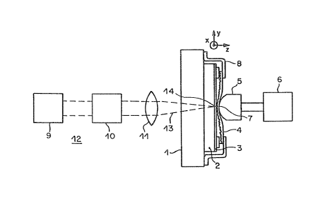
Figure 1 is a view showing the basic prin-
ciple of an apparatus for producing a surface
pattern,
~5 Figures 2 to 4 show various surface
~atterns,
Figure 5 shows a punch, and


B


Fig~re 6is a view showing the basic principle of an apparatus
for scanning a pattern original.
In Figure 1 which is not drawn to scale, reference numeral 1
denotes a flat, rigid and optically transparent pressure plate.
Secured thereto in a manner not shown in the drawing is an optically
tx~nsparent substrate 2. The surface of the substrate 2 which is
r~ote rom the pressure plate 1 is coated with a thin layer 3 of
ther~oplastic, radiation-absorbent material in which a macroscopic
s~^ace pattern with a microscopic stxucture, in particular a
ln stm cture having an optical diffraction effect, is to be embossed.
The layer 3 may comprise for example a plastics film or foil
which is black or coloured. It may also be formed by colouring the
surface of the substrate 2, for ex~nple by means of colloidal carbon,
in a plastics solution. The typical thickness thereof is from
1~ 0.1 to 10 ~m.
Disposed opposite the thermoplastic layer 3 is an unheated
embos-ing die 4 which has a microstructure which is to be reproduced in a
r~yion-wise manner, the die 4 comprising for example a nickel
alloy and advantageously being flexible such that by ~eans of a
~0 punch 5, it is possible to produce an embossing pressure which is
closely defined in terms of pressure per unit of surface area,
as bctween the embossing die 4 and the thermoplastic layer 3.
~he typical thickness of the embossing die is 100 ~m. A~vantageously,
the punch 5 nas a convex surface with a typical radius of
~5 curvature of about 7 mm. The punch S is pressed against the embossing
die 4 by means of a pressure generating means 6, and the embossing
die 4 is pressed against the thermoplastic layer 3 in the region
of a small contact zone 7, a typical diameter of which is 3 mm.
A die holder 8 which is only diagrammatically shown in Figure 1
holds the embossing die 4 in such a way that it only lies against
the thermoplastic layer 3 in the region of the contact zone 7,


and elsewhere is slightly spaced therefrom. The die holder ~ is
advantageously of such a configuration that the embossing die 4
can be turned with a small number of simple manual handling
operations or evèn by machine, or can be replaced by another embossing
die with a different microstructure when the pressure generating
means 6 is in the rest condition.
Disposed on the side of the pressure plate 1 which is remote
from the embossing die 4 is a beam source 12 which advantageously
comprises a laser 9, an optical modulator 10 and a lens system
11 and which focusses a focussed or concentrated thermal or light
keam 13 on a focal.spot 14 in the region of the thermoplastic
layer 3, which is substantially at the centre of the contact
zone 7. Due to absorption of the directly incident beam 13 and
the baam reflected at the embossing die 4, the layer 3 is
heated in the region of the focal spot 14. The typical diameter
of the focal spot 14 is less than 100 ~m. m e thermal or light
beam 13 may be controlled in respect of its energy, or cut in
al~d out, by means of the modulator 10
The pressure generating means 6 permits displacement of the
punch 5 in the z-axis which is normal to the surface of the
components 1 to 4. The ab~ve-described components of the apparatus
are mounted on a base plate (not shown3 in such a way that the
pressure plate 1, the substrate 2 with the thermoplastic layer
3 and the embossing die 4 can be displaced relative to each other
in a continuous or stepwise manner relative to the focal spot
14 and the punch 5 both on the x-axis and also on the y-axis,
that is to say, in a plane parallel to the thermoplastic layer
3. For that purpose, the components 1 to 4 may be arranged to be
displaceable and the components 5 and 12 may be arranged to be
stationary, or vice-versa. It is also possible for the conlponents
1 to 4 and 12 to be stationary and for the beam 12 to be caused


to follow the movement of the punch 5 in the x-y-plane by means
of a mirror system.
The embossing pressure is so set by means of the pressure
generating means 6 that in its cold condition, in the region of
tl~e contact zone 7, the thermoplastic layer 3 is adapted to the
microstructure of the embossing die 4 only with elastic deformation,
a~d wllen the embossing pressure is released, it relaxes back into the
original condition, that is to say, a smcoth condition. If on the
other hand the beam 13 is switched on simultaneously with the
application of the embossing pressure, the radiation-absorkent
thermoplastic layer 3 is heated above its softening temperature
in an approximately punctiform surface element which is in the
focal spot 14 of the source 12, the rise in temperature being to
such an extent that, in the above-mentioned surface element, the
lS surface of the layer 3 is plastically deformed to correspond to
the microstructure of the embossing die 4, and the embossed
structure is retained after cooling, when the embossing pressure
is removed. The desired surface pattern is now made up of a
multiplicity of such surface elements.
In the stationary writing mode, the beam 13 is only briefly
~witched on. The heated volume of the thermoplastic layer 3
then quickly cools dc~ by heat conductioninto the embossing die
4 and the punch 5 on the one hand, and the layer 3 and the substrate
2 repectively on the other hand. The pressure generating means 6
moves the punch 5 into the rest position and thus separates
the embossing die 4 from the thermoplastic layer 3. The embossed
structure is retained in the region of the focal spot 14. That
embossing procedure is now successively repeated insofar as,
between the individual embossing operations, with the source 12
switched off and the embossing pressure removed, the substrate
2 with its thermoplastic layer 3 is displaced relative to the focal


spot 14 and the punch 5 in the x-y-plane by a given amount in a
given direction. Between the individual embossing operations, the
embossing die 4 may be changed or it may be turned by a give~n
amount about the z-axis. In that way, regions of the layer 3
which are isolated from each other or which are joined together
may be provided with any desired microscopic structures.
In the dynamic writing mode, the embossing die 4 and the
substrate 2 with the layer 3 are continuously displaced at a
given spe~d relative to the Eocal spotl4 and the punch 5, with the
source 12 switched on and the pressure generating means 6 also
in an operative condition, so that interconnected strip-like
surface regions of the microstructure of the die are reprod~ced
on the layer 3. Any desired surface patterns with a microscopic
structure can also be produced by successive shaping, in the
dynamic writing mode.
The macroscopic surface patterns produced in accordance with
the described method may represent geometrical figures, numbers,
letters, ornaments, guilloches etc, whose microscopic structure
forms a single one or a plurality of different phase diffraction
gratings, phase holograms, kinoforms and the like. Thus it is
possible for example to produce in the thermoplastic layer, in an
economical fashion, a complex network or mesh of twisted and
sinuous macroscopic lines with a microscopic stnlcture having an
optical diffraction effect, wherein the microscopic stnlctures
change from one line to another or even vary for example in a
quasi-continuous fashion along a line, so that the human eye sees
the effect of guilloche patterns with moving colours. However, the
described method may also be used for example for producing finely
contoured microstructures, as are used in the art of what is
referred to as integrated optics.


Fron the surface pattern produced on the thermoplastic
layer 3, it is possible to produce a duplicate in the form of a
metal embossing die, using known chemical and galvanic procçsses,
with the embossing die thus produced being used for mass production
of the surface pattern in a conventional embossing apparatus.
Figure 2 shows, as a simple example of a surface pattern
which is produced in accordance with the described method, a
narrow band or strip which is produced by a single writing movement
on the y-axis. The width of the band or strip is approximately
equal to or slightly larger than the diameter of the focal spot
14 and is for example 50,um. The structure of the strip forms for
example a linear phase diffraction grating with 10 to 2000 lines
per millimetre.
By arranging such strips in a row, as shown in Figure 3, it
is possible to produce surface patterns of any desired size, with the
microscopic structures of adjacent strips merging into each other
without any dicontinuity. When a plurality of such strips are
disposed in juxtaposed relationship without the embossing die
4 moving relative to the layer 3, that produces a microscopic
structure whose structure lines extend continuously over a plurality
of strips, as can be seen from Figure 3.
As shown in Figure 4, a structure which has been produced can
he freshly written over. In that situation, the old structure is
erased if the energy density of the beam is at a sufficiently high
level. That simplifies the production of complex struc-tures as,
in a first writing operation, it is not necessary to exclude those
surface areas which are to be covered with another structure in
a subsequent second writing operation.
However, by precise quantitative control of the energy
density of the beam 13 and the speed of writing, it is also possible
for a new structure to be embossed over an old structure, without


in that operation the old structure being completely erased.
The advantages of the invention can now be readily seen.
As already mentioned, both very fine line or punctiform surfaces
and also interconnected surface portions of larger sizes can be
S provided with microstructures having an optical diffraction effect,
without visible join lines, by producing the microstructures in
ad~Qining relationship or by partially writing one microstructure
over another. The structure of the individual surface elements
of such surface patterns may be identical or may vary from one
element to another. It is also possible to produce microprofiles
which cannot be produced by interferometric methods. m e edges
of the embossing are sharply defined and do not have troublesome
bead portions. Generally speaking, the described metho~ is the
first to afford the possibility of synthesising finely contoured
microstructures, free from being bound to rigid mask systems,
wherein the operating procedure can be completely auto~ated by
numerical programming and control.
If the embossing pressure is produced by means of the punch S
exclusively in the region of the focal spot 14, undesired partial
~0 col~ defo~mation of the layer 3, upon pressure contact with the
embossing die 4 at locations where the microstructure is not to
be formed from the embossing die 9, is reduced to what is
absolutely necessary, in regard to duration and frequency, throughout
the total embossing time. In addition, changing the die is
~5 facilitated thereby, while in comparison with producing a pressure
over the entire surface, the embossing forces are substantially
lower, which makes it easier to arrive at the mechanical design
of the apparatus.
Figure 5 shows a punch 5' which comprises a ball holder 15
and a ball 16. The ball 16 is disposed with a sl~all amount of


clearance in a cylindrical space 17 in the holder 15. The longitudinal
axis of the cylindrical space 17 coincides with the z-axis (Figure
1). A part of the ball 16 projects out of the holder 15 and
forms the convex surface of the punch 5'. The space 17 communicates
with a ccmpressed air source 20 which acts as the pressure
generating means 6', by way of a compressed air conduit 18 and
an electromagnetic valve 19.
The increased air pressure in the space 17 presses the ball 16
against the embossing die 4 (Figure 1), can be cut in and out by
the valve 19~ and may be finely varied within wide limits, thereby
permitting precise adjustment of the embossing pressure. Automatically
cutting off the embossing pressure by means of the valve 19 makes
it possible easily to replace, turn or displace the embossing die
4. The fact that the ball 16 is supported by the air cushion at
its sides ensures that it suffers from a low level of resistance to
rolling movement. The leakage air which escapes between the ball
16 and the cylindrical walls of the ball guide member provides
for air cooling for the ball 16.
In Figure 6, reference numeral 21 denotes a graphic pattern
original whose macroscopic surface pattern 22 is scanned by an
optical-electronic scanning devi oe 23 and reproduced true to
scale as a macroscopic surface pattern with microscopic structure
on the layer 3 (Figure 1). A displacement unit 24 guides the
scanning device 23 comprising a light source, lens system and
light detector (not shown~ over the original 21, for example in a
line-for-line manner. Synchronously with respect thereto, the
focal spot 14 and the punch 5 are displaced relative to the layer
3 and the embossing die 4. In the drawing, that is indicated by
a lever system in the form of a pantograph 25 which is moved by
the displacement unit 24 and, in being so moved, is rotated about
a fixed pivot point 26. m e electrical output of the scanning device

.X6~ `34


23 is connected by way of an amplifier 27 and a threshold switch
28 to a control input 29 of the modulator 10 of the source 12.
If the losal reflectivity of the original 21 exceeds a
predetermined value, the modulator 10 is opened so that the
microstructure of the embossing die 4 is produced at the
~orresponding points of thè layer 3. In the case of a degree of
reflectivity which is below the predetermined value, in contrast,
there is neither permanent formation of the microstructure~ nor
~rasure of any structure which has possibly been previously
embossed.
The modulator 10 may also be controlled in such a way that
embossing does not occur at a high level of reflectivity of the
original 21, but at a low level of reflectivity. In addition, the
modulator 10 may be actuated in a gradual fashion instead of in a
binary fashion, while the dependency of the energy of the beam 3
on the reflectivity of the original 21 may be linear or non-
linear. Gradual actuation of the modulator 10 produces modulation
of the width of the embossed surface element.

Representative Drawing
A single figure which represents the drawing illustrating the invention.
Administrative Status

For a clearer understanding of the status of the application/patent presented on this page, the site Disclaimer , as well as the definitions for Patent , Administrative Status , Maintenance Fee  and Payment History  should be consulted.

Administrative Status

Title Date
Forecasted Issue Date 1990-02-27
(22) Filed 1985-06-27
(45) Issued 1990-02-27
Expired 2007-02-27
Correction of Deemed Expired 2007-06-12

Abandonment History

There is no abandonment history.

Payment History

Fee Type Anniversary Year Due Date Amount Paid Paid Date
Application Fee $0.00 1985-06-27
Registration of a document - section 124 $0.00 1985-11-25
Maintenance Fee - Patent - Old Act 2 1992-02-27 $100.00 1992-01-24
Maintenance Fee - Patent - Old Act 3 1993-03-01 $100.00 1993-01-26
Maintenance Fee - Patent - Old Act 4 1994-02-28 $100.00 1994-01-26
Maintenance Fee - Patent - Old Act 5 1995-02-27 $150.00 1995-01-30
Maintenance Fee - Patent - Old Act 6 1996-02-27 $150.00 1996-01-23
Maintenance Fee - Patent - Old Act 7 1997-02-27 $150.00 1997-01-24
Maintenance Fee - Patent - Old Act 8 1998-02-27 $150.00 1998-01-23
Maintenance Fee - Patent - Old Act 9 1999-03-01 $150.00 1999-01-25
Maintenance Fee - Patent - Old Act 10 2000-02-28 $200.00 2000-01-28
Registration of a document - section 124 $100.00 2000-02-15
Maintenance Fee - Patent - Old Act 11 2001-02-27 $200.00 2000-12-28
Maintenance Fee - Patent - Old Act 12 2002-02-27 $200.00 2001-11-29
Maintenance Fee - Patent - Old Act 13 2003-02-27 $200.00 2002-11-14
Maintenance Fee - Patent - Old Act 14 2004-02-27 $250.00 2003-11-13
Maintenance Fee - Patent - Old Act 15 2005-02-28 $450.00 2005-02-04
Maintenance Fee - Patent - Old Act 16 2006-02-27 $450.00 2006-02-06
Expired 2019 - Corrective payment/Section 78.6 $150.00 2007-01-31
Owners on Record

Note: Records showing the ownership history in alphabetical order.

Current Owners on Record
OVD KINEGRAM AG
Past Owners on Record
ANTES, GREGOR
LANDIS & GYR IMMOBILIEN AG
LGZ LANDIS & GYR ZUG AG.
Past Owners that do not appear in the "Owners on Record" listing will appear in other documentation within the application.
Documents

To view selected files, please enter reCAPTCHA code :


To view images, click a link in the Document Description column. To download the documents, select one or more checkboxes in the first column and then click the "Download Selected in PDF format (Zip Archive)" or the "Download Selected as Single PDF" button.

List of published and non-published patent-specific documents on the CPD .

If you have any difficulty accessing content, you can call the Client Service Centre at 1-866-997-1936 or send them an e-mail at CIPO Client Service Centre.


Document
Description 
Date
(yyyy-mm-dd) 
Number of pages   Size of Image (KB) 
Description 1993-12-07 11 470
Drawings 1993-12-07 1 34
Claims 1993-12-07 9 340
Abstract 1993-12-07 1 15
Cover Page 1993-12-07 1 19
Representative Drawing 2002-03-11 1 6
Fees 1999-01-25 1 30
Prosecution-Amendment 2007-01-31 2 66
Correspondence 2007-06-21 1 12
Fees 1999-01-25 1 28
Fees 1998-01-23 1 28
Fees 1997-01-24 1 39
Fees 1996-01-23 1 51
Fees 1995-01-30 1 46
Fees 1994-01-26 1 31
Fees 1993-01-26 1 23
Fees 1992-01-24 1 51