Note: Descriptions are shown in the official language in which they were submitted.
SC-5200-C
INTERRUPTING DEVICE WITH IMPP.OVED CURR~NT-LIMITING ARRANGEMENT
B~CKGROUND OE; THE INVENTION
Field of the Invention
The present invention relates to an improved interrupting device or
interrupter and an improved current-limiting arrangement that enables the transfer
of current from a main-current-path section into a current-limiting section com-prising a plurality of fusible elements. The present ;nvention is an improvement over
the arrangements disclosed and claimed in the following, commonly assigned U.S.
patent numbers: 4,359,708; 4,4819495; and 4,~67,307.
Description of the Related Art
The aforementioned patents ~,359,708 and 4,481,495 are directed to
high-voltage interrupt;ng devices and current-limiting fuses. As discussed in those
patents, the fusible elements disclosed therein are suitable for use in parallel with
the mnin current path of an interrupting device; one or more fusible elements com-
prising the current-limiting section of the interrupting device. An interruptingmodule utilizing one or more of the fusible elements of the aforementioned patents
and a main-current-path sec tion including a switch are disclosed in the afore-
mentioned U.S. patent number 4,467,307. The interrupting device as shown in the
'307 patent may include a common housing for the main-current-path section and the
one or more fusible elements; the one or more fusible elements being intimately
surrounded by compacted fulgurite-forming medium such as silica or sand. The
main~current-path section has a high continuous current rating and is designed to
carry much higher eontinuous currents than the current-limiting section. The
impedance of the main current path is much lower than the impedance of the
current-limiting section so that under normal conditions, with the main current path
closed, the main current path carries substantially all the current with only a
negligible portion of the current flowing through the one or more fusible elements of
~ - .. : ~
' ' ':' , . .
the current-limiting section. When an overcurrent condition exists, the switch in the
main-current-path section is operated to thereby create one or more gaps in the
main curterlt path. Upon the creation of the one or more gaps, the current then
commutates or transfers to the current-limiting section whereupon the one or more
fusible element~ melt and interrupt the current according to well-kno-~n principles.
The fusible element in U.S. patent number 4,359,70~ includes spaced
groups of holes with the separation between adiacent holes within each group being
substantially less than the separation between adjacent groups of holes. This
10 arrangement provides for suitable control of the rate of rise of the arc or bacl~
voltage after the fusible element has been completely burnt bacl~ in the area
between the individual holes within each group of holes; burn-back or melting of the
fusible element thereafter continuing between the groups.
The fusible element of U.S. patent number 4,481,495 also includes
groups of holes or notches with the width of the fusible element being greater
between the groups of holes or notches. Accordingly, the fusible element o~ the 'g95
patent makes use of the merged arcs within the groups of holes or notches as in the
'708 patent. Further, after the arcs have merged within the group, the rate of burn
20 bacl~ of the ribbon is further slowed due to the decrease in current density in the
element at the wider regions. ~ccordingly, the back voltage across the device isprevented from exceedirlg R selected value.
The interrupting device, for example, as disclosed in U.S. patent
number 4,467,307, is required to transfer Ol' commutate high currents from the main
current path to the one or more fusible elements of the current-limiting section.
Specifically, the maximum instantaneous current that can be transferred into the one
or more fusible elements can be a limiting factor regarding the maximum inter-
rupting capability of the interrupting device and the capability to interrupt high-
30 frequency currents. For suitable operation of the interrupting device at higheroperating voltages, the length of the fusible elements and the components of the
main current path are increased. Accordingly, the rapid transfer of current to the
one or more fusible elements is adversely affected due to the increase of the
:. :
9~
irnpedance of the one or more fusible elements and the reduced velocity of the
movable portion of the switch in the main-current-path section. Of course, if
melting of one or more of the ~usible elements takes place before the transfer o~
current from the main current path to the current-limiting section is complete,
successful interruption may not be accomplished.
Arrangements to improve the transfer of current from the main
current path to the one or more fusible elements are disclosed and claimed in co-
pending, commonly assigned Canadian Patent application Serial Numbers 513,007 and
513,011 filed in the name of Roy T. Swanson. The '011 application includes first and
second contacts arranged in telescoping fashion such that, upon rapid movement of
the first contact relative to the second contact, there is a delay in the creation of
the gap to allow the movable contact to accelerate to desirably high velocities
before significant arc voltages are generated by the creation of the gap. In the '007
application, energy absorbing means, such as a member fabricate~ from arc-
extinguishing material, is provided between an insulative piston and a movable
contact; the piston being arranged to be moved at high speeds to drive the movable
contact through the energy-absorbirlg member thereby preventing undesirable
dynflmic interactions and rebounding between the piston and the movable contact.
Either as an alternative to or as an extension of the arrangements in
these co-pending applications, to alleviate the dif~iculties encountered with
increasing voltage ratings related to the transfer of current from the main current
path to the fusible elements, the melting time of the fusible elements can be
increased such that higher heating effects of the current (I2t) are required before the
fusible elements melt. The increase in the I2t characteristic of the fusible elements
can be achieved by using thicker or wider fusible elements or by increasing the
number of fusible elements in the current-limiting section of the interrupting
device. Increasing the melting I2t of the fusible elements provides additional time
30 for the transfer of current from the main current path to the current-limiting
section before melting takes place.
:
: `' :'
,
~2~
While the increase in melting I2t of the fusible elements allows
additional time for the transfer of high currents from the main current path to the
current-limiting section before the melting of any of the fusible elements, the mini-
mum current that will melt the one or more fusible elements to accomplish inter-ruption is also increased. Additionally, at low overcurrents, the timc that is required
to melt the fusible elem ents will also be similarily increased. Accordingly,
increasing the I2t to melt the fusible elements by increasing the number of fusible
elements, or by using thicker or wider fusible elements, increases the minimum
current that can be cleared or interrupted by the interrupting device-- absent
specific facilities or instrumentalities to counter the increflse in the minimumclearing current.
Fusible elements including various patterns of holes or notches and/or
having various cross-sectional geometries or structure are also shown in the
following: U.S. patent numbers 2,8337891; 2,866,040; 3,863,187; 3,909,766; 4,123,738;
4,146,863; 4,150,354; 4,219,794; 4,204,184; 4,227,167; and 4,227,168; German publica-
tion 1,193,154; Canadian Patent No. 1,001,698; and Canadian Patent No. 1,010,483.
The a~orementioned U.S. Patent No. 4,123,738 in the Summary of the
Invention theleo~ recites a curr~nt-limiting fuse including a main fusible element
with an "M" spot (body of low melting temperature alloy) adjacent thereto, and an
auxil;ary fusible element across the main fusible element. The current-limiting fuse
is stated to include elements for significantly reducing the arcing time required to
clear low-magnitude fault currents without appreciably affecting the minimum
melting I2t value, the time-current curve, or the I2t let-through of the fuse. As
shown in FIG. 3 of the '738 patent, the main fusible element 38 includes a reduced
section 40 at the "M" spot and reduced sections 42 and 44 at the portions at which
the ends of the au~;iliary fusible element 30 are connected through respective arc-
gap electrodes 34,36. The sections 46, 48~ 50 and 52 of the main fusible element 38
between the reduced sections 40, 42 and 44 include a plurality of uniformly-spaced
circular perforations 26 to define fusion points of minimum cross-sectional areas
along the fusible element 38. For small but prolonged overload currents, the fusible
element 38 melts first at the "M" spot 28 ~FIG. 4b of '738). Due to the reduced
portion ~0, the fusible element 38 burns back at a much faster rate than the conven--
tional fuse element 1~1 of FIG. 1 of the '738 patent which is depicted as being of
uniform width and as having uniformly-spaced circular perforations 26. As the arc
voltage across the auxiliary element exceeds a given value, the gaps 3~,36 spark over
and current is diverted to the auxiliary fuse element 30 (FIG. 4c of '738). The arc
across the "M"-spot pol tion Oe the fusible element 38 eYtinguishes and the fuI~urite
about the portion 40 cools. The intensive heat of the arcs at arc-gap electrodes34,36 quickly burns open the reduced sections ~2,44 (FIG. 4d of '738); the rate of burn
bflck at the reduced portions 42 and 44 being higher than the rate of the conventional
fusible element 14. When the auxiliary element 30 vaporizes (FIG. 4e of '738), the
circuit is interrupted. ~or high magnitude fault currents, the reduced portions 40, ~2
and 44 and the fusion points of the sections 46, 48, 50 and 52 are stated to vaporize
almost instantaneously. While the arrangement of the '738 patent is alleged to
provide desirable results, the manufacture thereof for consistent operation would
appear to be rather complex as requiring a main fusible element of reduced cross-
sectional areas, an "M" spot, an auxiliary element formed by a fusible wire, and the
arc--gap electrodes 3~,36. ~lthough it is somewhat unclear, the t738 patent appears
to utilize two main tusible ribbons 14 or 38 to provide the main fusible element 12 of
the fuse 10. Similatily, two fusible wires 32 comprise the auxiliary fusible element
20 30.
While the aforementioned arrangements may be generally suitable for
their intended use, it would be advantageolls to provide an interrupting device with
an improved and easily manufacturable current-limiting section so as to enable the
transfer of higher currents from the mflin current path of the interrupting device
into the current-limiting section without substantially affecting the minimum
current that can be cleared or interrupted by the current-limiting section.
SUMMARY OF T~IE I V_NTION
Accordingly, it is a principal object of the present invention to provide
an improved interrupting device having an ;mproved current-limiting section for
providing the transfer of higher currents from a main current path Oe the inter-
~ ,. ... .
rupting device into a current-limiting section while not substantially increasing the
minimum current that can be cleared or interrupted by the current-limiting section.
It is another object of the present invention to provide an improved
interrupting device having a main-current-path section including a switch which is
operable to create one or more gaps in the main-current-path section and the inter-
rupting device further including a current-limiting section connected in parallel with
the main-current-path section; the current-limiting section including a plurality of
fusible elements, one or more of the fusible elements having holes or notches, the
10 remaining one or more fusible elements having holes or notches that are more
elongated than the holes or notches of the one or more fusible elements so as toachieve a desirably wide range of currents that can be interrupted.
These and other objects of the present invention are achieved by pro-
viding an improved current-limiting section for an interrupting device to achieve the
transfer of higher currents from a main-current-path section of the interruptingdevice into the current-limiting section which is connected in parallel with the main-
current-path section. The trans~er of higher curl ents is achieved without sub-
stantially increasing the minim~lm clearing culrent. The main-current-path section
20 of the interrupting device carries substantially all of the normal, load current while
only a negligible portion of the current ~lows through the higher-impedance current-
limiting section. The main-current-path section includes a switch that is operated
upon the occurrence of overcurrent conditions. Upon operation, the contacts of the
switch are rapidly separated to create one or more gaps. Upon the creation of the
one or more gaps, the current is transferred into the current-limiting section. The
current then melts the one or more fusible elements of the current-limiting section
in accordance with the melting 12t characteristics thereof. In one particular inter-
rupting device, the main-current-path section and the current-limiting section are
enclosed by a common housing. The current-limiting section includes a plurality of
30 fusible elements. The fusible elements are thin, elongated, conducti~te ribbons that
are disposed about the main-current-path section with the fusible elements being in
intimate engagement with a particulate, fulgurite-forming medium contained within
the housing. One or more of the fusible elements have a first predetermined pattern
~ , :'',,; '' ;;~
of reduced cross-sectional areas that is different than a second predetermined
pattern of reduced cross-sectional areas provided in the one or more remaining
fusible elements such that for low overcurrent conditions, the one or more fusible
elements having the second predetermined pattern melt ~nd have gaps created at an
earlier time than the one or more fusible elements having the first predetermined
pattern. At higll overcurrent conditions, the melting characteristics of the fusible
elements having the first predetermined pattern and the melting character;stics of
the fusible elements having the second predetermined pattern are substantially
equal. In a specific arrangement, one or more of the fusible elements include holes
10 of a first type and one or more of the remaining fusible elements include slotted
holes of a second type that are elongated aIong the length of the fusible element as
compared to those of the first type. For overcurrents in a low range, when the
switeh is operated and the current transfers to the fusible elements, the heat buildup
in the reduced ribbon portions adjacent the slotted holes of the second type is sub-
stantially greater than the heat buildup in the reduced portions adjacent the holes of
the first type. Accordingly, the one or more fusible elements with the slotted holes
of the second type melt Ol burn back more quickly than the one or more fusible
elements having holes Oe the first type. Additional current is then commutated from
the one or more fusible elements having the slotted holes of the second type into the
20 one or more fusible elements having the holes of the first type thereby decreasing
the time to melt and increasing the rate of burn-back therein. Thus, for over-
currents in a low range, since the overall melting time of the fusible elements is
shorter than it would be if all the fusible elements had holes of the first type, the
minimum clearing current is also lower. At high overcurrents, the melting times of
the fusible elements are so short that the dit`ference in heat buildup around the holes
of the first type and the slotted holes of the second type is negligible so that all the
fusible elements exhibit similar melting times. This arrangement provides suitable
arc-voltage characteristics whereas the use of fusible elements which all have
slotted holes of the second type makes the transfer of current into the fusible
30 elements more difficult due to the higher impedance and results in unsuitable,
undesirably high arc-voltage characteristics; the one or more fusible elements in the
:. . ,
:
. ..
9~
arrangement having holes o~ the first type exhibiting lower arc-voltage characteris-
tics as the fusible element melts as compared to the fusible elements having slotted
holes of the second type.
BRIEF DESCRIPT~ON OF THE DRAWING
The invention, both as to its organization and method of operation,
together with further objects and advantages thereof, will best be understood byreference to the accompanying drawing in which:
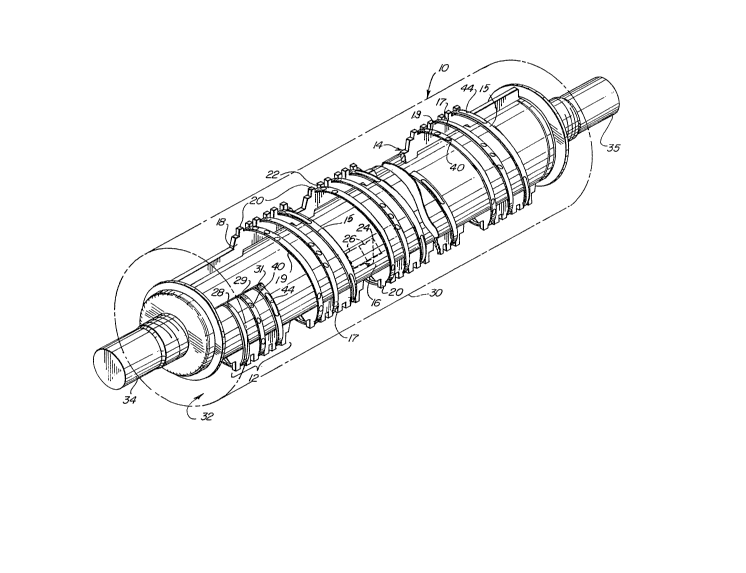
l0FIG. 1 is a perspective view of a high-voltage interrupting device which
includes a current-limiting section according to the present invention;
FIGS. 2 and 3 are elevational views of respective fusible elements of
the current-limiting section of FIG. I;
FIGS. 4 and 5 are elevational views depicting the fusible elements of
FIGS. 2 and 3 respectively after current has been transferred to the fusible elements
and burn back or melting of the ~usible elements has begun;
20FIG. 6 is an elevational view of an alternate embodiment of the fusible
element of FIG. 3; and
FIGS. 7 and 8 are elevat;onal views of alternate fusible elements.
DETAI D DESCR1PTION OF E INVENTION
Referring now to FIG. 1, the interrupting device 10 of the present
invention includes a current-limiting section 12. The current-limiting section 12
includes a plurality of fusible elements. For example, in the specific, illustrative
30embodiment of FIG. 1, the current-limiting section 12 includes three fusible
elements 15, 17 and 19. Each of the fusible elements is a thin, elongated conductive
ribbon. The fusible elements 15, 17 and 19 are held in a circular, helical configura-
- - . , - ,
~ . ,
. . .
3~
tion by an element support 14. A hollow, insuIative cylinder 16 is provided which
cflrries fins 18 oî the support 14. The fins 18 include a series of projections 20
having notches 22 about which the fusible elements 15, 17 and 19 are wound~
The interrupting device 10 includes a normally-closed switch that is
schematically represented at 24 and thflt defines a main current path of a main-current-path section. The switch 24 includes one or more pairs of contacts 26 which
are relatively movable apart along a fixed line of direction within the cylinder 16.
Various portions of the interrupting device 10 are shown only generally, and some
10 portions thereof are shown only in phantom for the sal~e of clarity. The interrupting
deYice may be generally as described in U.S. Patent No. 4,467,307 for suitable
pract;ce of the present invention. The ends 28, 29 and 31 of the respective fusible
elements 15, 17 and 19 are electrically connected in shunt with the contacts 26 by
suitable facilities (not shown); for example, as disclosed in the aforementioned '307
patent. The interrupting device 10 has a high ContinllOUS current rating for which the
main current path is designed and the impedance of the main current path throughthe switch 24 is much lower than the impedance of the current~limiting section 12.
~ccordingly, with the contacts 26 closed, substantially all of the current flowsthlough the switch 2~ while only a negligible portion of the current flows through the
20 current-limting~ section 12. In response to an overcurrent condition, the switch 24 is
opened by rapidly separating the contacts 26 whereupon the current is commutatedor trans~erred from the main currerlt path to the cllrrent-limiting section 12.
The interrupting device 10, in the specific, illustrative embodiment of
FIG. 1, includes an outer housing 30 of insulating material which de~ines a volume 32
with the cylinder 16; the volume 32 being filled with a fulgarite-forming medium (not
shown) such as silica sand or quartz. When the current is transferred to the current-
limiting section 12, the fusible elements 15, 17 and 19 and the medium co-act, as is
well known, to interrupt the current in a current-limiting or energy-limiting
30 mannerO The interrupting device 10 is mountable and electrically connectable into
an electrical circuit (not shown) by end terminals 34,35 which may protrude beyond
' ~
: ': ' `
3~
the ends of the cylinder 16 and the housing 30. Each of the terminals 34,35 is elec-
trically connected to a respective end 28, 29 and 31 of the fusible elements 15, 17
and 19 and a respective contact ~6 in any convenient manner.
In accordance with important aspects of the present invention, one or
more of the fusible elements of the current-limiting section 12 includes a firstpredetermined pattern of holes of a first type or geometry and the one or more
remaining fusible elements includes a second predetermined pattern of holes o~ asecond type or geometry. With this arrangement, the interrupting device l0, while
l0 also being capable of trans~erring higher currents from the main current path to the
current-limiting section 12, provides a minimum clearing current that is desirably
low while also being capable of transferring higher current from the main current
path to the current-limiting section 12. For example, for suitable operation of the
interrupting device 10 at higher operating voltages, the length of the fusible
elements and the components of the switch 26 are increased. Accordingly, the trans-
fer of current from the main current path to the current-limiting section 12 is
adverse1y affected due to an increase in the impedance of the fusible element and
the reduced velocity of the movable portions of the switch 24. The melting time of
the fusible elements of the currerlt-limiting section 12 cAn be increased such that
20 higher heating effects of the current (T2t) nre required before the fusible elements
melt, thus allowing mole time for the transfer of the current. l-lowever, if themelting I2t of the fusible elements of the current-limiting section 12 is increased by
increasing the number of fusible elements or by using fusible elements of larger cross
section, the minimum clearing current is also increased as is the minimum current to
melt the fusible elements. On the other hand, if all fusible elements such as 15 are
utili~ed, the transfer of current to the fusible element is adversely àffected due to
the higher impedance of the fusible elements and the arc-voltage characteristics are
undesirably high.
In accordance with the current-limiting section 12 of the present
invention, at least one of the plurality of fusible elements of the current-limiting
section 12, for example fusible element lS, is provided with a pattern of holes that
causes the fusible element 15 to exhibit a shorter melting time at low current than
-- 10 -
one or more of the remaining fusible elementsO Specifically, and referring
additionally now to FIG~. 2 and 3, if the fusible element 17 is provided with a pattern
of holes 40 of a first type, the fusible element 15 is provided with a pattern of
slotted holes 44 of a second type. The fusible element 19 may then be provided with
a pattern of holes of either the first or second type or a different type as will be
discussed in more detail hereinafter. In the illustrative specific embodiment of FIG.
1, the fusible element 19 is identical to the fusible element 17 and is provided with a
pattern of holes 40 of the first type. In any case, at low currents, the one or more
fusible elements (e.g. 15) with the pattern of holes of the second type melts first
which then causes additional current to ~low through the remaining one or more
fusible elements (e.g. 17,19) having the pattern of holes of the first type.
In the specific embodiment illustrated in FIG. 1, the fusible elements
17,19 as best seen in FIG. 2, each include a series of slots or holes 40 of the first
type located in serial groups 42, while the fusible element 15, as best seen in FIG. 3,
includes a series of slotted or elongated holes 44. ~t low overcurrents, when the
switch 24 is operated and the current is transferred to the current-limiting section
12, the reduced-width sections 48,49 adjacent the elongated holes 44 of the fusible
element 15 are heated more rapidly by the current therethrough than are the corre-
sponding s~ctions 50,51 of the fusible etements 17,19 due to the heat loss or transfer
from the sections 50,St to the adjacent portions 52,53 of the fusible element 17. The
sections 48,49 of the fusible element 15 have grently increased heat buildup relative
to the sections 50,51 of the fusible element 17. Accordingly, the fusible element 15
at the sections 48,49 melts or burns back more rapiclly than the sections 50,51 of the
fusible elements 17,19. After the sections 48,49 of the fusible element 15 have
burned back so as to create gaps 60 as illustrated in FIG. 5 and the fusible elements
17,19 have burned back so as to create gaps 61 illustrated in FIG. 4, additionalcurrent is then commutated from the fusible element 15 to the fusible elements
17,19 thereby increasing the rate of burn-baclc in the fusible elements 17,19. For
high levels of overcurrents, the melting times of the fusible elements 15, 17, and 19
are short and substantially equal so that the difference in heat buildup is negligible
for each of the portions 48,49 compared to portions 50,51.
-- 11 -
....
' '
Accordingly, the tr~nsfer of high currents to the fusible elements 15,
17 and 19 and tile melting time thereof at high currents is substantially equal to that
for three fusible elements of the type 17. Thus, for ovcrcurrents in a low range,
since the overall melting time of the fusible elements 15, 17 and 19 is shorter than it
would be if all the fusible elements were of the type 17, the minimum clearing
current is also lower. The use of the fusible elements 15, 17 and 19 provides suitable
arc-voltage characteristics whereas the use of three fusible elements of the type 15
results in unsuitable, undesirably high arc-voltage characteristics as well as
increased difficulty in transferring current into the fusible elements due to the
10 increased impedance of the fusible elements; the fusible elements 17,19 exhibiting
lower arc-voltage characteristics as the fusible element melts as compared to fusible
elements of the type 15.
In the specific ernbodiment illustrated in FIGS. 2 and 3, the spacing
between groups 42 of the holes ~0 is substantially equal to the spacing between the
elongated slots 44. Further, the overall expanse of each group 42 is substantially
equal to the length of each elongated slot 44. Additionally, the transverse width of
the holes 40 and 44 measured across the width of the fusible elements are sub-
stnntially equaL
Referring now to FIG. 6, the fusible element 15' is identical to that of
the fusible element 15 of FIG. 3 e~cept that the elongated slots ~' of the fusible
element lS' are fabricRted with rungs or bridges 70,72 for ease of handling of the
fusible elements 15' during manufactule and for increased mechanical strength.
However, the melting characteristics of the fusible element 15' are substantially
identical to those of the fusible element 15 since the rungs or bridges 70,72 do not
significantly change the current density or heat transfer of the sections 48,49.
While there have been illustrated and described various embodiments of
30 the present invention, it will be apparent that various changes and modifications will
occur to those skilled in the art. For example, while the holes 40 are depicted in
FIG. 2 as being generally circular with flattened or straight portions adjacent the
sections 50,51 and while the elongated slots or holes 44 are depicted as rectangular
,`
~, .
''
with oval ends, it should be realized that the holes may have other shapes or may be
replaced by notches; that is regions of any shape formed in or through the fusible
elements 15,17. Additionally, while the holes ~10 and 44 are illustrated as being
generally centered about the res?ective longitudinal axes 62,64 of the fusible
elements 15,17, the holes 40 and ~L~ need not be so centered. Further, the holes or
notches 40,4-1 need not e.~tend completely through the fusihle elements 15,17 but
need only effectively reduce the cross-sectional area o~ the fusible elements 15,17 at
the points of formation thereof. The features of the present invention are provided
by the melting time of one or more of the fusible elements of the current-limiting
10 section 12 ~eing substantially less at low currents than the one or more remaining
fusible elements while the melting time at high currents is substantially the same for
all the fusible elements. In the specific embodiment of the current-limiting section
12 oE FIG. 1, the fusible element 15 includes elongated slots of the second type while
the fusible elements 17,19 include holes of the first type. ~Iowever, as noted herein-
before, the desired features of the present invention are achieved by the provision of
a patterrl of s;tes of reduced cross-sectional area for one or more of the fusible
elements to provide a reduced melting time at low currents compared to one or more
of the remaining fusible elements; i.e., the invention can be practiced in specific
embodiments with more than two dit`~erent types of hole geormetries and more than
20 two difEerent hole geometries ~or any o~ the fusible elements. ~dditionally, the
fusible elernents in specific ernbodiments may incorporate the features depicted in
the aforemerltioned '495 and "l08 patents. The use of notches instead of holes is
illustrated by the fusible elements 76 and 78 of F1GS. 7 and 8 respectively. Further,
while a specific embodiment of the interrupting device 10 has been described forillustrative purposes, it should be realized that many other specific embodiments are
also possible for the practice of the present invention utilizing the improved current-
limiting section 12. For e~cample, the fusible elements 15,17 need not be helical
configurations. It is intended in the appended claims to cover all such changes and
modifications as fall within the true spirit and scope of the present invention.
- 13 --
'