Note: Descriptions are shown in the official language in which they were submitted.
~63~5
BACKGROUND
The present invention relates to
microwave antennas, and more particularly to planar
antennas for circularly polarized waves.
A number of designs have been proposed for
high frequency planar antennas, particularly with
respect to antennas intended to receive satellite
transmissions on the 12 GHz band. One previous proposal
is for a microstrip line feed array antenna, which has
the advantage that it can be formed by etching of a
substrate. However, even when a low loss substrate such
as~teflon)or the like is used, there are considerable
dielectric losses and radiation losses from this type of
antenna. Accordingly, it ia not possible to realize
high af~iciency. and also when a substrate is used having
a low loss characteristic the cost is relatively
expensive.
Other proposed antenna designs are a radial
line slot array antenna, and a waveguide slot array
antenna. These antennas tend to have reduced dielectric
and radiation losses, as compared to the microstrip line
feed array antenna. However, the structure is relatively
compllcated, so that production o~ this antenna design
becomes a difficult manufacturing problem. In addition,
since each of these designs are formed as a resonant
structure, it i5 very difficult to obtain gain over a
~ ~ - 2 -
:
.
:
..: ,.
... : ~ , ,
32~i
wide pass band, for example 300 to 500 MHz. Furthermore,
these designs are complicated by the cost of coupling
between slots, which makes it very d:Lfficult to obtain a
good efficiency characteristic.
Another proposal is for a suspended line fePd
aperture array. This design has a structure which
overcomas some of the foregoing defects, and can also
provide a wide band characteristic, using an inexpensive
substrate. Suspended feed line antennas are illustrated
in MSN ~Microwave System News), published March 1984, pp.
110-126.
The antenna disclosed in the first of the above
applicat1ons incorporates copper foils which have to be
formed perpendicularly relative to both surfaces of a
dielectric sheet which serves as the substrate. Since
the structure is foxmed over both surfaces of the
substrate, the interconnection treatment becomes
complicated, and the antenna is necessarily relatively
large in size.
The antenna disclosed in the other above-cited
application requires copper foils to be formed on two
separate dielectric sheets. It is difficult to get
accurate positioning of these foils, and the construction
becomes relatively complicated and expensive. I~ the
- 3 -
:
.~
..
.. . .
,,
, ~
, . .
,
. .
-
325
antenna disclosed in the MSN publication, one excitation
probe is formed in each of a plura:lity of openings to
form an antenna for a linear polarized wave. Such an
antenna cannot effectively be ussd to receive a circular
polarized wave, because the gain is poor, and two
separate substrates must be used, making the construction
relatively complicated and expensive.
BRIEF DESCRIPTION OF THE PRESENT INVENTION
A principal object of the present invention is
to provide a circular polarized wave planar array antenna
in which a pair o~ excitation probes are formed in a
common plane on a single substrate, to transmit or
receive a circular polarized wave, while attaining
simplicity of construction, low-cost and excellent
performance characteristics. In accordance with one
embodiment of the present invention, a substrate is
sandwiched between conductive lay~rs having a plurality
of openings, with a pair o~ perpendicular excitation
probes being located in alignment with each opening, with
signals from the xcitation
.:
'' .
~ 3a -
~'
~:.
, . , ~ , .
,- ,
:: : - :
.-.: . .~. ~
ii32~;
probes being combined in a predetermined phase relationship with
each other.
In a development of the invention, two additional
conductive elements are provided in alignment with tne excitation
probes to provide improved impedance matching relative to the
openings in the conductive layers.
In a further development of the invention, a connection
network is associated with each pair of excitation probes,
comprising a pair of feed lines each having length of a quarter
wavelength and a rssistance element intersonnected between such
feed lines.
In another development of the present invention, the
feed point of the an-tenna array is located near the center
thereof, and occupies the position normally occupied by one of
the pairs of excitation probes.
BRIEF DESCRIPTION OF THE DRAWINGS
Reference wi]l now be made to the accompanying drawings
in which:
Fig. 1 is a top view of a cixcular polarized wave
radiation element cons-tructed in accordance with one embodimen-t
of the present invention;
Fig. 2 is a cross-sectio~al view of the apparatus of
Fig. 1 taken along the line I-I;
Fig. 3 is a cross-sactional view of one of the suspended
line sections of the apparatus of Figs. 1 and 2, taken along the
line II-II in Fig. 2;
Fig. 4 is a top view of one of the radiation elements of
the antenna of one embodiment of the present invention, showing
the suspended lines for feeding the excitation probes;
Fig. 5 is a plan view illus-trating the interconnection
of a plurality of radia-tion elements;
..
: . .. .. . ,:
. .
.. .. ..
.
.,
,
~26~32S
Fig. 6 are frequency characteristics of embodiments of
the present invention;
Fig. 7 is a functional block diagram illustrating the
manner of connection of a plura'ity of sub-arrays;
Fig. 8 is a graph indicating a radiation pattern o-f one
embodiment of the present invention;
Fig. 9 is a top view of a modified form of the radiation
element, illustrating a network for feeding the excitation
probes;
Fig. 10 is a plan view of a portion of the apparatus of
Fig. 9;
Fig. 11 is an e~uivalent circuit diagram of the
apparatus of illustrated in Figs. 9 and 10;
Fig. 12 is a fre~uency characteristic of the radiation
element of embodiments o'f ~he invention; and
Figs. 13 and 14 are plan views of two modified
interconnection diagrams for central feeding of a plurality of
radiation elements.
BRIEF DESCRIPTION OF THE P~EFERRED EMBODIMENTS
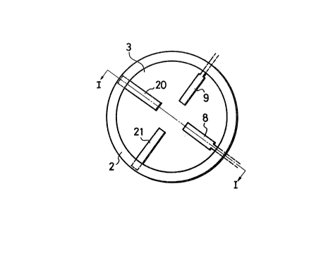
Referring to Figs. 1 and 2, an insulating a substrate 3
is sandwiched between metal layers 1 and 2 (which may be formed
of shest metal such as aluminum or mstalized pl-astic). A number
of openings 4 and 5 are formed in the layers 1 and 2, the opening
4 being formed as a concave depression or recess, in the layer 1,
and the opening 5 being formed as an aperture in the layer 2.
Fig. 1 has a plan view of -the structure.
A pair of ~xcitation probas 8 and 9, oriented
perpendlcular to each other, are formed on the substrate 3 in a
common plane, in ali~nment with the~openings 4 and 5 as
illustrated in Fig. 1. The excit-ation probes 8 and 9 are each
connected with a suspended line conductor 7 located wi-thin a
_5_
, ~ : :.. "
-, : , -
.: : ~ ' -
.. . . . .
, . . . .
. ; :: ;- ........... -
; ' - ~ .
.
,~
~6~25
cavity 6 which forms a coaxial line for conducting energy between
the excitation probes 8 and 9 and a remote point. The substrate
8 is in the form of a thin flexible film sandwiched between the
first and second metal or metalized sheets 1 and 2. Preferably,
the openings 4 and 5 are circular, and of the same diame-ter, and
the upper opening 5 is formed with a conical shape is illustrated~
in Fig. 2.
The suspended line conductor 7 comprises a conductive
foil supporte~ on the substrate 3 centrally in the cavity portion
6 to ~orm a suspended coaxial feed line. A cross-section of this
suspended line is illustrated in Fig. 3. The foil 7 forms the
central conductor and the conductive surface of the sheets 1 and
2 form the outer coaxial conductor.
Fig. 4 i].lustrates that the conductive foil 7 is formed
into elongate feed lines, arranged perpendicular to each other,
where they are connected to the excitation probes 8 and 9, and
connected together by a common leg. The foils are connected to a
feed line at the point 11, which is offset relative to the center
of the common leg, as shown in Fig. 4, so that the excitation
probe 9 is fed by a line having a longer length, indicated by
reference numeral 10, of one quarter of wavelength, relative to
the length of the feed in the excitation probe 8. The wavelength
referred to here (and elsewhere in this application) is the
wavelength of energy within the waveguide or suspended line 7,
indicated by A/g, which wavelength is determinable from the
frequency of the energy and the geometry of the waveguide. With
this arrangement, (considering the antenna as a transmitting
antenna) a circular polarized wave results, as the result of
linear polarized waves launched from excitation probes 8 and 9
which are out of phase by lr/2, or one quarter wavelength.
Preferably, the foil 7 is formed as a printed circuit by
etching a conductive surface on the substrate 3, so as to remove
-6-
:
,:
2~i
all portions of -the conductive surface except for the conductive
portions desired to remain such as the foil 7, and the excitation
probes 8 and 9, etc. Preferably, the conductive foil has a
thickness of, for e~ample 25 to 10~ micrometers. Since the
substrate 3 is thin and serves only as a support member for the
foil 7, even though it is not made of low loss material, the
transmission loss in the coaxial line is small. For example, the
typical transmission loss of an open strip line using a teflon-
glass substrate is 4 to 6 dB/m at 12 G~z, whereas the suspended
line of the invention has a transmission loss of only 2.5 to 3
dB/m, using a substrate of 25 micrometer in thickness. Since the
flexibla substrate film 3 is inexpensive, compared with the
teflon-glass substrate, the arrangement of the present invention
is much more economical.
As illustrated in Fig. 4, the phase of the signal
applied to the excitation probe 8 (as a traffsmitting antenna) is
advaneed by a quarter of the wavelength (relative to the center
frequency of the transmission band~ compared with that applied to
the excitation probe 9. This arrangement, when used as a
receiving antenna, allows a clockwise circular polarized wave to
be received, since the excitation probe 8 comes into alignment
with the rotating E and H vectors of the wave one quarter cycle
after the excitation probe 9 is in such alignment. Beeause of
the inereased length 10 o~ the foil line connected with the
exeitation probe 9, the exeitation probes 8 and 9 eontribute
nearly equal in-phase eomponents to a composite signal at the T
or combining point 11.
:
~ If the extra length 10 were inserted in the foil line 7
, :
connected with the excitation probe 8, then the arrangament would
receive a counter-clockwise circular polarized wave. It would be
appreciated that this can be effectively accomplished merely by
turning over the sheet 3 on which the excitation probes 8 and 9
--7--
` '
.
:
~ ,
.
.. . .
3~
and the feed lines 7 are supported, so that the structure of the
present invention can receive both kinds of circular
polarization, with slight modification during assembly.
Fig. 5 illustrates a circuit arrangement in which a
plurality of radiation elements, each like that illustrated in
Figs. 1-4, are interconnected by foil lines printed on the sheet
3. Each of the radiation elements contributes a signal in phase
with the signal contributed by every other radiation element,
which are interconnected together at a point 12. It will be
appreciated from an examination of Fig. 4 that the length of the
foil line 7 from the point 12 to any of the individual excitation
probes 8 and 9, constitutes an e~ual distance, so that the
signals received from each radiation element arrive at the point
12 in phase with the others. The array of Fig~ 5 shows the
printed surface on the substrate 3,:and the aligned position of
the openings 5 in the sheét 2. The substrate 3 is sandwiched
between the conductive sheets 1 and 2 having the openings 4 and 5
(Fig. 2) aligned with each of the radiation elements, so that all
of them function in the manner described above in connection wi-th
Figs. 1-4. Using the general arrangement illustrated in Fig. 5,
it is possible to obtain various radiation patterns, by changing
characteristics of the lines. For example, if the distance from
the common feed point 1~ to the excitation probes 8 and 9 of some
of the radiation elements is changed, the phase of the power
contributed by those radiation elements can be changed. Further,
if the ratio of impedance is changed by reducing, or increasing,
the thickness of the suspended lines at the places where it is
brancned (as shown in Fig. 5) it is possible to change the
amplitude of the signals contributed from the branches to the
common line of -the branch. This affects the relative power and
phase of the signals contributed from each of the receiving
-8-
, ~ ~
:;: ` .
.
i3;2~i
elements, with the res~lt of changing the radiation pattern of
the antenna.
Although the antenna is asymmetrical on the common
plane, an isolation OL more than 20 dB is established between
probes at a frequency of 12 GHz, with a return loss being as low
as 30 dB. The axial loss approximates about 1 dB in the vicinity
of about 12 GHz.
Fig. 7 illustrates the construction of a large circular
polarized array, using a plurality of the array subgroups
illustrated in Fig. 5~ Sixteen arrav groups 13a-13p are all
interconnected at a common point 14, in such a fashion that the
length of the in-terconnecting lines are all equal. In this case,
the antenna is formed with 256 circular polarized wave radiation
elemen-ts, arranged in an equi-spaced rectangular array, and each
element is located at an equal distance from the feed poi,nt 14.
; Fig. 8 shows a radiation pattern which is characteristic
of the arrangement illustrated in Fig. 7. In this case, the
distance between the radiation elements is selected to be 0.95
(at a frequency of 12 GHz), and the phase and amplitude are
selected to be equal for all radiatlon elements. Since the
mutual coupling between the radiation elements is small, the
characteristic is highly directional, as shown.
Because of the construction of an antenna in accordance
with the present invention, the antenna can be made very thin,
and with a simple mechanical arrangement. Even when inexpensive
substrates are used, the gain obtained from the antenna is equal
:
to or greater than that of an antenna which uses the relatively
expensive microstrip~line~substrate technology.
When the spacing of the radiation elements is selected
in the range from 0.9 to 0.95 wavelength relative to a 12 GHz
wave in free space (ranging from 22.5 to 23.6 mm), the width of
~ .
` the cavity portion for the suspended line is selected as 1.75 mm,
' '''' ' . _g.
,: ,
.
:' ~
3~5
and -the diameter of the openinys 4 and 5 in sheets 1 and 2 is
selected as 16.35 mm. However, for most effective reception of
the satellite broadcasting frequency band (11.7 to 12.7 GHz) it
is desirable to select the line width to be wider than 2 mm, and
a reduced diameter of the radiation element. For example, for
most effective reception, the diameter it must be reduced from
16.35 to about 15.6 mm.
However, if the diameter of the radiation element is
selected as small as 15.6 mm, the cut-off frs~uency of the
dominant mode (TEll mode) of the circular waveguide having this
diameter becomes about 11.263 GHz. As the result, it becomes
difficult to achieve impedance matching between the cavity
portion formed by the openings 4 and 5 and the excitation probes,
and the antenna becomes relatively narrow in band width. Thus,
the characteristic of the return losses change. This is shown by
the broken line a in Fig. 6, with the result that the return loss
near the operation frequency (11.7 to 12.7 GHz) and
`~ deteriorates. The "return loss" refers to the loss resulting
from reflection due to unmatched impedances. With this
applioation therefore, better impedance matching is necessary.
This matching is provided in the arrangement of Figs. 1-5 by the
US9 of conduotive segments 20 and 21 which are aligned with
excitation probes 8 and 9 within each radiation element. These
elements, as shown in Figs. 1 and 2, are aligned end to end and
~in line with the excitation probes 8 and 9 and spaced apart
: ~ :
;~ therefrom, as shown in Figs. 1 and 4~ The conductive segments 20
and 21 are elongate, rectangular and are formed as printed
circuits or otherwise deposited on the surface of the substrate
3. They extend beyond the perimeter of the opening 5 to be in
electrical contact with the layer 2. The use of the segments 20
and 21 makes it possible to lower the cut-off frequency of the
radiation element, and to improve the return loss to that shown
' -10-
:
,: :
- : :
.
. .
.. ::..:-
.
32S
in the solid line b of Fig. 6. When the optional conductive
segments 20 and 21 are not used, the probes 8 and 9 are in the
same positions, relative to the openings 4 and 5. In that case,
the return loss characteristic is about -30 dB at minimum, with a
narrower pass band characteristic, l.e. a steeper fall off from
the minimum. The isolation between the coupling probes 8 and 9
is greater than 20 dB, as shown in Fig. 6, so the radiation
element effectively receives circular polarized radiation in the
same manner as described above. When the radiation elements are
spaced apart by 23.5 mm, as illustrated in Fig. 5, then an array
of 256 radiation elements, arranged in the manner of Fig. 7,
forms a square of 40 cm by 40 cm.
It will be appreciated, that because of the reciprocity
principle of an antenna, the radiation elements of the antenna of
the present invention function equally effectively as
transmitting radiation elements, and receiving radiation
elements. Thus, the antenna array of the present invention can
function effectively as a transmitting or receiving antenna
~, ~
array.
; Because of the conductive segments 20;and 21, the cut-
off frequency is lowered, so that the matching can be established
to improve the return loss from the dashed line a of Fig. 6 to
the solid line b of Fig.~ 6. When the diameter of the openings 4
and 5 of the~radiation element is selected as 15.6 mm, then a
wavegulde having a~small~dlameter~c~an~be used, and the i;mage
suppresslon is improved.`
It is possible to 1mprove;;the~standlng wave ratio ~VSWR)
at~the~T sectlon 1l where~the;two~foils 7 from the e~ci-tation
elements~ are~lnterconnected~to~a~common feed line.~ With the T
branching arrangement, a portion of a wave received from~one of
the excitation probes pa~sses through the~T toward the othe~
excltation probe, with the result that the axial ratio of -t~
~ .26~3~S
circular polarized wave is deteriorated. The axial ratio is a
ratio (for an elliptically polarized wave) between the diameters
OI the major and minor axes of the elipse representing the
polarization. For a circular polarized wave, the a~ial ratio is
1.
In the arrangement OI Fig. 4, when the two signals to be
combined are not equal in amplitude and phase, then signals in
the two legs are not balanced, and a combining loss is
generated. A combining loss is also generated when the impedance
connected between the combining terminals is not matched, which
degrades the axial ratlo of the circular polarized wave.
Fig. 9 illustrates a radiation element with an improved
T combiner, surrounded by the dashed line a. An enlarged view of
the area within the dashed line a is illustrated in Fig. 10. The
common feed line 7 is indicated in Fig. 10 as a leg A, with legs
B and C leading to the excitation probes 8 and 9. A printed
resistor 42 is placed on the substrate interconnecting the legs B
.,
and C. Between the printed resistor 42 and the common leg A, the
foil line 7 is separated into a pair of one quarter wavelength
:
lines 40 and 41, which interconnect the common leg A with the
legs C and B, respectively. The resistor 42 is formed, for
example, by carbon printing on the sub9trate. This circuit forms
what may be called Wilkinson-type power combiner or a 3 dB.~/2
hybrid ring-type combiner. In a case where the impedances of all
three legs A,~B and C are matched wi-th each other, and power is
~upplled~from a leg C, then one quarter of the;power is passed
through the printed resistor 42, and three quarters of the power
ls passed through to the llne 40. Of;the pover passed to the
line 40, two thirds of this is supp}ied to the leg A, with the
rema~inder (namely, one fourth of the~origlnal supplied power)
being passed through the line 41. Since the two components
passed through the resistor 42 and through the line 41 are e~ual
-12-
, .: ., - :
.
:.,. .. : , ::
, .: :
: -:............. :
~2~3%~
and opposite in phase, they substantially cancel each other out,
with the result that there is no power which reaches the leg B
from the leg C. Accordingly, the isolation between the legs 3
and C becomes about -25 d3, with an improvement in the axial
ratio.
The equivalent circuit of the combiner of Figs. 9 and 10
is shown ln Fig. 11. This equivalent circuit is based on the
theory of a Wilkinson-type power divider, as described in "An
N-Way Hybrid Power Divider", IEEE Trans. Microwave Theory in
TechO, MTT-8, 1, p. 116 [Jan. 1960), by E.J. Wilkinson. Here, Z0
represents the characteristic impedance of the feed line, and the
characteristic impedance of Z0 at the legs B and C is matched to
the impedance of the radiation element. When the impedance at
all three legs are matched, the input rom the leg A is divided
with a certain ratio, and appears at the input and output
terminals B and C. In the case of an input from the terminal B,
a part of -this input appears at the terminal A, with remaining
part being absorbed by the resistor 2 Z0, so that the
corresponding power is not generated at the terminal C. The
y-type power~combiner can achieve the isolation between the~
terminals while allowing the power received at the terminals~B
and C to be combined at the terminal A.
Fig. 12 shows the characteristic of the aircular
:
~ polarized wave radiation element, in which the solid line
.: :
indicates an example of measured results of the axial ratio of an
an-tenna~wlthout the comblner or~Figs. 9 and;10, while the solid
line B indlcates the measured regults of the axial ratio when a
straight T combiner is used. For e~amplej at a frequency of
about~12 GHz,~an axi;al ratlo of~about;l dB is tolerable, meaning
that, when used as a~transmltting antenna, the transmitted po~ier
at;tlmes~spaoed by1~/2 does not vary~by~more than 1 dB. ;As 3hown
in line b o Fig. 12, this igure ls;realized over a broad
3 ~ ~
.~ : , ~ , :: :
~: .
~2~i32~
frequency band. Line a shows the characteristic when the
combiner of Figs. 9-10 is nct used.
With the closely packed radiation elements llus~rated
in Figs. 5 and 7, it is dif~icult to provide a Iesd point at the
center of the array, so the feed point must be brought out to the
outer edge of the array as shown. This results in a rela~ively
longer feed path, with attenuation of the signal. It is
desirable to couple the array to a standard rectangular waveguide
such as type WR-75 or WRJ-120.
2eferring to Fig. 13, an array is lllustrated in which a
central feed is supplied to a plurality of circular polarized
wave radiation elements, all in phase, from a feed point 12. All
of the radiation elements are located at the same dis-tance from
the feed point 12 by means of the foil 7 connecting the central
point 12 to the probes 8 and 9 of each radiation element 2. In
the arrangemen-t of Fig. 13, one the radiation elements closest
the center of the array is removed, and a rectangular waveguide,
the outline which is shown in rectangular dashed box 30, is ;
attached~to the array at this point. The transiti~on from a
rec-tangular waveguide to the coaxial line (shown in cross-section
in~Fig. 3) is made in the conven-tional way and therefore need not
be described in detail. A resis-tor 31 is provided to terminate
the line normally connected to the removed radiation element with
the characteristic impedance of the feed line, to avoid any
reflectlon effect from the removal of this radiation element. By
using~the arrangement of Fig. 13, the length o~ the feed line
becom~es~shorter than that shown~in Plg. 5. For a larger array,
such as~that of Fig. 7, each of~the sub-arrays of array Flg 7 is
made~up of~an array~l1ks~that of Fig.~5, for example. One of the
four sub`-arrays closest to the center of the array has one
radiation element~(at its corner nearest the center) omitted, and
-14-
. . : -, , : :
::: ' ~ '
3~S
that radiation el~ment is replaced by a feed connection leading
to the branch at the array center, and a terminating resistor 31.
The conversion loss or such an arrav is relatively low,
and the arrav can be connected to a normal rect2ngu7ar
waveguide. This advantage increases in importance when the array
structure has more radiation elements. The fact that the
radiation pattern is disordered to a minor extent by the removal
of one radiation eIement does not represent a serious effect in
practice. Particularly when there is a large number of radiation
elements, excited in e~ual phase and equal amplitude, the ef~ect
of the removal of one radiation element is small. Furthermore,
the central feeding arrangement allows a more convenient
structure in which the waveguide 30 is centrally located.
Fig. 14 shows an alternative feeding circuit, ln which
the wiring of the feed line of the central portion is partly
changed so aæ to provide space for a rectangular waveguide shown
in outline by the dashed block 32, without removal of a radiation
element. The width of the waveguide 32 is indicated in Fig. 14
as a, and lts helght is indicated as b. It is generally
preferable that b = a/2. However, because of the spacing of the
; radiation elements, the height b must be shorter than the normal
height. As a result, the characteristic impedance within the
waveguide becomes lower, the length of the waveguide 32 must be
kept short,~and it is~difficult to obtain matching over a wide
band. It~ls~also dlfficu~lt to~reduce the lnsertion loss of the
arrangement illustrat~d ln~;Fig. 14.~All of these dlsadvantages
are~overcome-~by the deslgn;of Fig. 13.~
By~the foregoing, it w~ be~ appreclated that the
present~lnventlon constitutes~a~simple and economical form of
microwave~antenna. It~ls apparent~that various addltions;and
modiflcations may be made~ in the apparatus of the present
nvention wi~thout departing from the essentlal~features of
~ 15-
:.':
~6~3~5
- novelty thereof, whlch are intended to be defined and secured by
the appended c1eims.
.
,~
: c: , ~
:l~ :: :
:~ , : - - :