Note: Descriptions are shown in the official language in which they were submitted.
727
APPARAT~S AND ~ETHOD FOR TD~ DATA SWITCHlNG
The present invention relates generally to TD~
data switching and, more particularly, to a novel
apparatus and method for full duplex data switching
between TD~ buses in accordance with the time slot or
channel to which each data component is assigned.
BACKGROUND OF THE INVENTION
Telephone switching systems typically
constitute a switching network for temporarily
establishing transmission paths between various pairs
of subscribers. When one subscriber calls another, a
path is established between the two subscribers which
is an actual electrical path or which, in more
sophisticated systems, acts like one. Traditionally,
the switching network has been designed to switch
analog voice signals between the subscribers using
known pulse code modulated (PC~) time division
multiplexing (TDM) techniques.
In the switched public network telephone
system, a two wire subscriber loop, often called a
"twisted pair", connects a subscriber's telephone to a
central office switch. The subscriber loop carries an
analog voice signal. The central office switch pulse
code modulates the voice signals from active loops and
time multiplexes these pulse code modulated signals to
effect switching between active subscriber loops and
establish a point-to-point connection between two
subscribers. In addition, TD~ trunk lines interconnect
the central offices with each other to effect switching
between subscribers served by different central
offices.
Increasing levels of interoffice traffic have
been accompanied by increasing use of digitized
interoffice trunks. The digitization of interoffice
communications has had the effect of allowing more TD~
channels to be carried on each TD~ trunk so that each
q~
~Z~672~7
--2--
central office may serve increasing numbers of
subscribers and so that higher quality service may be
provided to the subscribers. Of course, the central
office PC~-TD~ switches have to interface with the
digital interoffice network. Accordingly, there has
been a trend to digitize the central office switches.
However, this t~end has not been universal. Therefore,
many central offices still retain the PCM-TDM switches.
Irrespective of ~he character of the central
office switch, the subscriber loop has, in nearly all
public telephone systems, remained a strictly analog
portion of the existing switched public network.
Therefore, although digitization of switching and
communications at the central office has allowed the
quality of the basic service to continually improve,
the subscriber loop portion of the typical telephone
service has remained relatively unchanged.
Recently, there have been many proposals and
attempts to digitize the subscriber loop. A primary
impetus behind digitizing the subscriber loop is to
provide the subscriber with integrated services in a
fully digital telephone network. Such integrated
services would include, for example, the ability to
have a mix of medium speed and low speed data
communication channels which could be in use
simultaneously with one or more voice communication
channels. The proposed integrated services digital
networks (ISDN's) would operate on existing two wire,
twisted pair subscriber loops, although other vehicles
such as optical fiber are also possible. A most
apparent advantage of ISDN is that the existing network
of subscriber loops would not have to be replaced, nor
would they have to be supplemented by additional
twisted pair loops to provide the integrated services.
Another advantage of the ISDN approach is that the
subscriber loop would not have to be selected for
~2~7~7
-3-
either voice or data communications to the exclusion of
the other. In the analog loop, data communications
must be coupled through a modem to the excl~sion of
voice communications.
As proposed in typical ISDN systems, the low
speed data communication channels would be useful for
vendors of certain services, such as home security and
alarm services. The medium speed data communication
channels would be useful for connection to packet
assembler/disassembler (PAD) vendors, such as the
Telenet and Tymnet services. In most existing
telephone systems, if such services are provided, all
of these vendors must interface through the existing
subscriber loop to the exclusion of the voice channel
or through an additional subscriber loop in which a
point-to-poin~ telephone connection can be established.
Integrated services digital networks, on the other
hand, provide the subscriber far greater flexibility
than is now possible with the existing analog
~0 subscriber loop. An example of a telephone system
providing integrated voice and data services over
twisted pair subscriber loops is described in applicant's
U.~. Patent No. 4,716,562, issued December 29, 1987.
In designing an integeated services digital
network, it becomes necessary to provide at the central
office the capability of demultiplexing the digitized
voice and data channel information received from each
subscriber loop and to switch each voice and data
channel to the intended recipient. Since many central
office switches cannot switch pure digital data, it
often becomes necessary first to terminate the
subscriber loop to perform a first order demultiplexing
which switches out and converts the voice bits received
--4--
from the subscriber loop to pulse code m~dulated (PC~)
analog bits for application to the existing central
office switch. The PC~ encoded voice may then be
switched and routed in a conventional manner. The
termination may also take the data bits from the
subscriber loops and multiplex these onto a TDM bus.
The TDM data containing several data channels from each
subscriber loop must then be switched to other TDM
buses which serve the data services vendors or other
intended recipients. To avoid duplication of hardware,
it is desirable that the data be switched in a full
duplex mode so as to be capable of switching concurrent
bidirectional data between the subscriber loops and
data services vendors or other intended recipients.
SU~MARY OF THE INVENTION
Accordingly, it is an object of the present
invention to provide a novel method and apparatus for
switching data between TDM buses.
It is an important object of the present
invention to provide a novel method and apparatus for
switching data wherein the data components within the
TD~ data stream are of different speeds.
It is a further object of the present
invention to provide a novel method and apparatus for
full duplex switching between TDM data buses.
According to the present invention, data is
switched between a plurality of first TDM buses and a
plurality oE second TD~ buses by sequentially receiving
successive data words from each of the first TD~ buses
for a predetermined time interval. Each of the data
words substantially upon receipt is written into one of
a first set of predetermined memory locations. The
stored words are then read in a predetermined order and
the presently read data word is written onto a data
bus. Substantially simultaneously with the present
data word being written onto the data bus, the data bus
~\~
Ei6~
--5--
is read and the word is stored in one of a second set
of predetermined memory locations. The predetermined
memory locations in the second set correspond to
particular time slots within each of the predetermined
s time intervals. The rearranged memory may then be read
and the presently read data word written to one of the
second TD~ buses which is currently enabled in the
reading time slot.
In a preferred form of the present invention,
the memory locations are in a plurality of memory
units, each of which is divided into four quadrants.
As data is being received from the first TD~ buses and
read into a first quadrant of each memory, prior stored
data may be read from a second quadrant of the memory
and written onto a backplane data bus. Substantially,
simultaneously therewith, the data is read from the
backplane data bus into a third quadrant of the memory,
while data stored in a fourth quadrant is written to
the second TDM buses. Data is read into a quadrant
until the quadrant is full, and is then swapped to
another quadrant in the memory for read out.
A particularly useful aspect of the present
invention for telephone systems is that one such
backplane data bus may be coupled to a plurality of
quadrant configured memories. Since each memory may
handle a plurality of TDM buses, the amount of data
switched on the data bus may serve a large number of
end users as is typically required for telephone
applications.
These and other objects advantages and
features of the present invention will become more
apparent from the following description when read in
conjunction with the drawings and the appended claims.
BRIEF DESCRIPTION OF THE DRAWINGS
FIGURE 1 is a schematic block diagram of a
portion of a telephone system central office;
~266~2~7
FIGllRE ~ i5 a data format diagram associated
with the operation of the central data switch cage of
FIGURE 1.
FIGURE 3 is a schematic block diagram of the
central data switch cage of FIGURE l;
FIGURE 4 is a schematic block diagram of each
switch card of FIGURE 3;
FIGURE 5 is a memory map of the TD~ memory of
FIGURE 4;
FIGURE 6 is a memory map of the configuration
memory of FIGURE 4; and
FIGURE 7 i~ a schematic block diagram of the
supervisor card of FIGURE 3.
DESCRIPTION OF THE PREFERRED EMBODI~ENT
Referring now to FIGURE 1, there is shown a
schematic block diagram representative of a portion of
a telephone system central office incorporating the
central data switch cage 10 constructed according to
the principles of the present invention. The switch
cage 10 is controlled by a master supervisor 11 as
described below. Connected to the central data switch
cage 10 in the central office are a plurality of loop
cages 12, a plurality of low speed gateways 14, and a
plurality of medium speed gateways 16.
Each loop cage 12 provides a termination for a
plurality of twisted pair subscriber loops 18. Each
subscriber loop 18 couples a remote multiplexer (not
shown) located at the subscriber premises to the
central office loop cage 12. Functionally, the remote
multiplexer multiplexes the digital voice and data
channels for transmission along the associated
subscriber loop 18 using time compression multiplex
(TC~) transmission format. The remote multiplexer is
fully described in applicant's U.S. Patent No. 4,730,311,
3S issued March 8, 1988.
~2~
--7--
The loop cage 12 demultipl~xes the TCM signals
generated by each remote multiplexer and transmitted
over the associated subscriber loop 18 by first
separating the voice channels from the digital data
channels. Typically, the information flows to and from
the remote multiplexers in a series of alternate
direction bursts. The loop cage 12 also may convert
the digital voice channels in each received burst into
analog voice channels for application to a conventional
central office switch (not shown) over twisted pairs
20. In the case of a digital central office switch,
the voice data may remain in digital format. As a
further alternative, voice data may be switched in the
central data switch cage 10 along with the other data
as described below. The loop cage 12 further
multiplexes the digital data channels received from
each of the subscriber loops 18. In a preferred
embodiment of the present invention, one TDM bus 22
couples three loop cages 12, hereinafter referred to as
a loop tri-cage 24, to the central data switch cage 10.
Each low speed gateway 14 demultiplexes data
received from the TDM bus 22 associated therewith for
distribution to a data services vendor. In the
preferred embodiment, the interface between the data
services vendors and the low speed gateway is an X.25
interface. Conversely, each low æpeed gateway 14
multiplexes data received from the X.25 interfaces for
transmission over the TDM bus 22 associated therewith
to the central data switch cage 10. The low speed
gateway 14 is fully described inllapplicanL~s u.S. Pa~ent No. .
4,706,241, issued November 10, 1987.
Similarly, each medium speed gateway 16
demultiplexes data received from the TDM bus 22
i;7%7
--8--
associated therewith for distribution to a data
services vendor In the preferred embodiment, the
interface between the data services vendor and the
medium speed gateway is a conventional packet
assembler/disassembler (PAD) interface. Conversely,
each medium speed gateway 16 multiplexes data received
from the PAD interfaces for transmission over the TD~
bus 22 associated therewith to the central data switch
cage 10. In a preferred form of the invention, the
medium speed gateways 16 are substantially identical in
function and arrangement to the loop cages 12.
The TD~ buses 22 connecting the central data
switch cage 10 to the low and medium speed gateways 14
and 16 are identical to the TD~ buses 22 coupling each
loop tri-cage 24 to the central data switch cage 10.
The TDM bit rate, frame size, and the frame rate and
frame period are identical for these buses. Therefore,
any reference hereinafter to TD~ buses 22 shall include
the buses connecting the data switch 10 to any of the
loop tri-cages 24, low speed gateways 14 and medium
speed gateways 16. An advantage of making each bus 22
identical regardless of its termination from the data
switch 10 is that any mix of devices may be
accommodated within each central office. In this
respect, there is no requirement for a set number of
loop tri-cages 24 or low and medium speed gateways 14
and 16. It is thus a clear advantage of the present
invention that it provides great flexibility in
configuring the data communication paths of each
central office.
In a preferred embodiment, each input TD~
channel from the loop tri-cage 24 carries data from up
to 144 subscriber loops 18 with each subscriber being
allotted four low speed subchannels and one medium
speed digital subchannel. If the switch cage 22 is
also used for voice switching, the subscriber may also
;`72~7
g
be alloted two voice subchannels, which may be switched
as described below for the medium speed digital
subchannels. Each medium speed gateway 14 uses a TD~
bus for up to 216 medium speed subchannels. Each low
speed gateway 14 uses a TD~ channel for up to 1,728 low
speed subchannels. A system can be configured with
loop tri-cages 24 and medium and low speed gateways 14
and 16 as desired. The system also allows other
devices to be coupled to the data switch cage 10 over
TD~ buses 22.
Furthermore, as will be described in greater
detail hereinbelow, since each TD~ bus 22 is identical,
data communications need not just occur between a loop
tri-cage 24 and one of the low or medium speed gateways
14 and 16. The data communication path through the
central data switch cage 10 can occur between any of
the TDM buses 22 including both directions on the same
TD~ bus 22. For example, data communications may occur
between individual subscribers coupled to separate loop
cages 12 such that the data switch 10 will switch data
between the respective loop cages 12. The data switch
10 may also switch digitized voice data, as well as
other data, between one or more loop cages 12 along the
TDM buses 22. Similarlyr data may be switched between
~5 separate PAD's through the central data switch cage 10.
Therefore, the present invention is useful in other
applications as well as part of a telephone switching
system. The present invention is the novel method and
apparatus embodied within the central data switch cage
10, as hereinbelow described.
To understand the overall operation of the
central data switch cage 10 and the present invention,
it is necessary to describe the preferred overall
timing relationships of the input and output data
strings, as well as the internal timing of the central
data switch cage 10. The entire system runs
--10--
synchronously under control of a 16.384 mHz backplane
clock signal provided by a suitable main timing control
(not shown) on the switch supervisor card 33 (FIGURE
3). Each TD~ input is a 2.048 megabit per second
serial data stream organized as shown in FIGURE 2. It
consists of 64 frames of 256 bits per frame. The first
four bits of each frame are used for framing signals
and the remaining 252 bits represent 28, 9 bit bytes.
Hereinafter such 9 bit byte quantities are referred to
as ~nytesn.
Each frame is 125 microseconds long with 64
frames constituting a superframe eight milliseconds in
length. The nytes from up to 72 TD~ channels are
collected and subsequently output onto a central data
1~ switch backplane bus (described below), 9 bits
parallel, at a 16.384 meganyte per second rate.
The input and output data buses, being
identical in format, run synchronously within the
central office at 2.048 megabits per second. Each
input TDM channel carries data allotted ~o low speed
and medium speed digital data channels (and voice if
desired). ~he design of the data switch 10 may support
up to 72 TDM channels. These TD~ input channels ~ay be
from any number of sources as long as the data arrival
times at the data switch 10 interface are maintained in
synchronism with the basic system timing reference of
the central office. Generally, each data switch cage
10 includes 12 switch cards and an associated switch
supervisor card. Each switch card is configured to
accept six TD~ channels. The TDM data is organized in
eight millisecond superframes. As described in greater
detail below, a data component switched through the
data switch cage 10 adds two superframe times or
sixteen milliseconds to the data path.
The central data switch cage 10 (FIGURE 3), in
the preferred embodiment. includes of a plurality of
~Z~6'7~
data switch cards 31 supported by a backplane bus 35.
Twelve positions are for switch cards 31 and one is for
the switch supervisor card 33. A second bus 37 is
provided for redundancy. Each card 31, 33 communicates
with the high speed bus 35, 37 on the backplane. The
switch cards also connect with the TD~ cable connector
to provide access to the TDM busses 22. The TD~ cables
plugged in here go directly to the gateways and
loopcages (FIGURE 1). The switch supervisor card 33
has a TDM cable connector 39 for communication with the
master supervisor 11 ~FIGURE 1) and a suitable control
and management system (not shown).
The TD~ channels 22 interface with the switch
cards 31, which communicate with each other over the
high speed backplane bus 35. The switch supervisor
card 33 provides all the timing and control pulses for
the switch cards 31, backplane 35, 37 and TD~ 22
channels.
The data from all the 72 TD~ channels appears
on the high speed backplane bus during the same
interval as a single superframe, that is the eight
millisecond superframe period. Each TD~I bit time
encompasses eight backplane nyte time positions and
thus each nyte time is coincident with 72 backplane
nyte times. To allow for a switch card to switch
quadrants as described below, the first nyte position
of frame 1 and the last nyte position of frame 64 are
not used, as shown in the CDS-TD~ data format of FIGURE
2.
The capacity of the switch high speed back
plane bus is derived from converting the nytes from
serial bits to nine parallel bits on the bus 35, which
is nine parallel wires. This increases capacity by a
factor of 9. In addition, a 16 mHz bit frequency is
used instead of 2 mHz as on the TD~ buses for a factor
of 8 increase in capacity. Thus, ?2 TD~ channels can
2t7
-12-
be accommodated over backplane bus 35.
A switch cage backplane ~not shown), serves to
interconnect the switch cards 31, and the supervisor
card 33 as well as providing a path for the ~DM signals
to go from the switch cards to the TD~ buses. As best
seen in FIGURE 4, a low speed supervisor bus 39 is
provided to interconnect the supervisor card with the
switch cards to supervise the memory mapped in the
switch card memories for the low speed data.
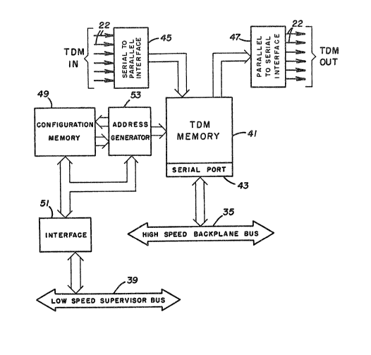
As may also be seen in ~IGURE 4, each switch
card 31 includes a TDM memory 41 connected to the high
speed back plane bus 35 via a serial port 43. A serial
to parallel interface 45 and a parallel to serial
interface 47 couples the TD~ memory to the TDM channels
22. A configuration memory 49 interacts with the low
speed supervisor bus 39 through an appropriate
interface 51 to operate an address generator 53. The
address generator 53 is coupled to the TD~ memory and
provides control over the location in which the various
data words are stored in and read out of the TDM memory
41. The TDM memory~ in the preferred embodiment, is
comprised of four quadrants. The total amount of
information which may be stored in one quadrant is
referred to hereinafter as a galactic rame.
~5 In FIGURE 5, a simplified block diagram of the
central data switch card memory data flow section is
shown. In a preferred embodiment, each card 31 i5
configured with a multiported 262,144 by 1~ bit memory
410 This memory is capable of storing four full
galactic frames. During each superframe, the following
data transfers occur simultaneously:
1. Serial TDM data for six input TDM buses is
converted to parallel and stored into a
quarter of the switch card memory;
2. Parallel data from another quarter of the
switch card memory is read and converted to
serial and output as six output TDM buses;
3~ A copy of an entire galactic frame from
the backplane bus is stored into another
quarter of the switch card memory; and
4. The fourth quarter of the switch card
memory is used to drive the high speed
backplane bus with selected nyte positions~
As best seen in FIGURE 5, after the lapse of
each galactic frame time, the assignment of the switch
card memory quarters i5 altered. The TDM input area
and the backplane output area swap places. Similarly,
the TD~ output area and the backplane input area swap
places. This may be simply accomplished by changing
the state of the most significant bit of the addresses
for each of these quarters.
Addressing of the switch card memory 41 is
accomplished by the address generator 53 providing
sequential access, refresh, and TDM and channel mapped
addresses. This address generator works in conjunction
with the configuration memory 49 which maps the nyte
position of the six TDM buses into the switch card
memory 41 and thus into the galactic frame. The
interface 51 from the configuration memory to the low
speed backplane bus 39 provides co~munication with the5 switch cage supervisor card.
In the preferred embodiment, the configuration
memory 49 consists of 24,576 words of 24 bits each.
The layout of the configuration memory is shown in
FIGURE 6. Each of the six TDM buses consist of 1,792
nyte positions in each superframe. A memory location
or address for each nyte position of each TDM bus is
needed for each direction (TDM channels in and out) for
full duplex switching. The resulting 21,504 locations
are used to hold the addresses of nyte positions of the
switch card memory 41. Thus each nyte position of a
TDM channel corresponds to the nyte storage location in
6~7%Y
the switch card memory and hencev also corresponds to
locations in the high speed backplane bus galactic
frame. The configuration memory is loaded by the
switch cage supervisor over the low speed backplane bus
39. The TD~ input positions and the TD~ output
positions are offset by one nyte position.
The switch cage supervisor illustrated in
FIGURE 7, shows the supervisory processor section 55
with its interface 57 to the low speed switch cage
supervisor bus 39 for communication with the switch
card configuration memories. A timing generator 59
provides all timing signals on the supervisor bus 39 to
operate the switch memories and TDM channel over the
high speed backplane bus 35.
In operation, the data switch of the invention
accepts time division multiplexed data channels from a
plurality of input data buses and selectively
multiplexes these inputs onto a common high speed
internal bus from which the data may be demultiplexed
~0 for distribution back onto TD~ channels leading to
other locations. This is accomplished by organizing
the incoming data into a series of galactic frames
which are then dumped onto an internal or backplane bus
serving the memory. The galactic frame on the
backplane bus is then restored in the memory in a
desired order for subsequent readout back to the TD~I
buses O
More particularly, a nyte arriving at one of
the switch cards 31 is stored at a particular location
in a ~uadrant of the memory of that switch card. The
particular storage location is determined by the switch
; supervisor card 33 which, in turnr is instructed from
the master supervisor 11 (FIGURE 1). Once the memory
quadrant in which the nyte is stored is full, the
memory swaps the entire galactic frame in that quadrant
to a read-out quadrant of the memory, from which it is
r~
read out, nyte by nyte in the order in which the nytes
were stored and in parallel format, onto the nine-wire
backplane bus 35.
Once on the backplane bus, each nyte is read
out to a particular location in a quadrant of a memory
in the same or a difference switch card connected to
the bus. The specific switch card to which the nyte is
routed is once again determined by the switch
supervisor as set by the master supervisor. Once that
quadrant is filled with a galactic superframe of nytes
from various other locations, it is swapped into a
read~out quadrant of the same memory. From there, the
nytes are read out serially onto a particular one of
the TDM buses in an order determined by the switch
supervisor card, as instructed by the master
supervisor.
Thus the sorting function of the switch takes
place at three levels: the input to the switch cards
from the TDM buses (according to location in the
galactic frame assembled in memory), the read out from
the backplane bus (according to the switch card to
which the nyte is routed, and the output to the TDM
buses from the switch cards (according to the order in
which the nytes are read out from memory and the
particular TDM buses onto which each nyte is routed).
This, coupled with the fact that a further sorting
function can be performed between several switch cages
through appropriate routing of TD~ buses, provided a
very rapid and reliable means for switching digital
information.
It may be seen, therefore, that the invention
provides an improved and novel time division multiplex
data switch which provides for full duplex data
switching between TDM buses in accordance with the time
slot or channel to which each data component is
assigned. Data of different speeds is readily handled
~;26~
-16-
in a simple and reliable arrangement and at extremely
high speed.
Various modifications of the invention in
addition to those shown and described herein will
S become apparent to those skilled in ~he art from the
foregoing description and accompanying drawings. Such
modifications are intended to fall within the scope of
the appended claims.