Note: Descriptions are shown in the official language in which they were submitted.
` ~
~Ei72~
1 53,109
ELEVATOR COMMUNICATION CONTROLLER
BACKGROUND OF THE IMVENTION
-
Field of the Invention
The invention relates in general to elevator
sy~tems, and more specifically to communication control
apparatus ~or controlling the communication between an
elevator bank controller and remote elevator fixtures.
Description of the Prior Art
Elevator systems require ast, accurate communi-
cation between the central elevator bank controller which
controls a bank of elevator cars and the various remotely
located elevator related fixtures. These fixtures include
the hall call pushbuttons and associated indicator lamps
located at each floor of the building, the up and down hall
lanterns located at each floor, digital or horizontal car
position indicators and status panels located at selected
floor~, and the various elevator car located functions such
as the door controll~r, car position indicator, direction
arrow~, and the car call pushbuttons and associated indica-
tor lamps.
To reduce manufacturing, installation and mainte-
nance costs while increasin~ communication speed and
accuracy, it would be desirable to provide a new and
improved universal elevator communication controller which
will hand}e any elevator fixture function it is dedicated
to. The universality has the economic advantage of being
able to place the communication controller on a single IC
6~Z~
2 53,109
chip which may be mass produced to provide an attractive
unit cost.
SUMMARY OF THE INVENTION
Briefly, the present invention is a new and
improved addressable elevator communication controller
which may be used for either floor controller type func-
tions (FC), or for position indicator type functions (PI),
simply by selecting the logic leveJ. applied to a single
input terminal. The data link from the central elevator
bank controller requires only three differential pairs of
wires, with one pair being a message clock line controlled
by the bank controller, another pair being for messages
prepared by the bank controller which are addressed to a
specific communication controller (input messages), and the
remaining pair being for messages prepared by the remote
communication controllers destined for the elevator bank
controller (output messages). Communication controllers of
both the FC and PI modes are connected to the same data
link, even though the input messages for the two modes have
different bit links. Output messages from both modes have
like bit lengths.
Eull duplex communication is provided between the
bank controller and the remote communication controllers,
i.e., the clock pulses which clock an input message to an
addressed communication controller simultaneously clock an
output message from a communicakion controller to the bank
controller. If the input message being clocked is referred
to as message number X, the simultaneous output message is
alway~ from the communication controller which received the
immediately prior input message, i.e., message number X-l.
In order to discriminate between line noise and
valid information in the data link, each communication
- controller include~ digital correlators which sample the
clock and input message lines at a rate which is substan-
tially higher than the clock and message rate. Eachdigital correlator saves the last N samples. Whan a
predetermined number of the last N samples has a
~i6~7~
3 53,109
predetermined logic level, the output of the correlator
changes logic levels. The new output logic level from the
correlator persists until the number of saved samples
having the predetermined logic level falls below the
S predetermined number.
BRIEF DESCRIPTION OE THE DRAWINGS
The invention may be better understood, and
further advantages and uses thereof more readily apparent,
when considered in view of the following detailed descrip-
tion of exemplary embodiments, taken with the accompanyingdrawings in which:
Figure 1 is a block diagram of an elevator system
having a plurality of communication controllers connected
to an elevator bank controller;
~igs. lA-lE illustrate message formats which may
be used in the elevator communication system of Fig. 1;
Fig. 2 is a detailed block diagram of a communi-
cation controller constructed according to the teachings of
the invention, which may be used for each of tha communi-
cation controllers ~hown in block form in Fig. l;
Fig. 3 is a schematic diagram of a digital
correlator constructed according to the teachings of the
invention, which may be used for the digital correlators
shown in block form in Fig. 2;
Fig. 4 is a graph which illustrates the operation
of the digital correlator shown in Fig. 3;
Fig. 5 is a schematic diagram of a parity check-
ing circuit which may be used for this function which is
shown in block form in Fig. 2;
Fig. 6 is ~ schematic diagram of a ring counter
and divider which may be used for this function which is
shown in block form in Fig. 2;
Fig. 7 is a schematic diagram of an enable
circuit which may be used for this function which is shown
in block form in Fig. 2;
4 53,109
Fig. 8 is a schematic diagram of a shift register
and data latch circuit which may be used for this function
which is shown in block in Fig. 2;
Fig. 9 is a schematic diagram of a parity bit
generator which may be used for this function which is
shown in block form in Fig. 2;
Fig. 10 is a schematic diagram of a multiplexer
and driver circuit which may be used for this function
which is shown in block form in Fig. 2; and
Fig. 11 is a graph which illustrates the multi-
plexing function performed by the circuit shown in Fig. 10.
DESCRIPTION OF THE PREFERRED EMBODIMENT
Referring now to the drawings, and to Figure 1 i~
particular, there is shown an elevator system 20 which may
have communication controller~ constructed according to the
teachings of the invention. Elevator system 20 includes
one or more elevator cars, such a~ elevator car 22 mounted
in a buildiny 24 having a plurality o floors, such as the
first floor 26, an uppermost floor 28 and a plurality of
intermediate floors, such as the second floor 30. The
elevator car3 are under the supervision of a group or bank
controller 32 which is in two-way communication with the
car controller of each elevator car, such as car controller
34 associated with elevator car 22. Car controller 34, for
example, may include a car position indicator 36, a door
controller 3&, car call control 40 and various other car
functions, shown yenerally at 42, such as the control for
detecting hatch switches.
Bank controller 3~ is also in two-way communica-
30 tion with the elevator fixtures located at the variousfloors at the building 24. For example, the first floor 26
may include an up hall call pushbut-ton and associated
indicator lamp, shown generally at 44, an up hall lantern
46, and a status panel 48 which includes a position indica-
tor for each elevator car. The second floor 30, and otherintermediate floors, include up and down hall call pushbut-
tons and associated indicator lamps, shown generally at 50,
2~
53,109
and up and down hall lanterns 52. A digital or horizontal
car position indicator 54 may also be provided. The
uppermost floor 28 includes a down hall call pushbutton 56,
an indicator lamp 58 associated with pushbutton 56, a down
hall lantern 60, and a car position indicator 62.
In accordance with the teachings of the inven-
tion, the elevator controller 32 communicates with the
various elevator fixtures and functions via one or more
data links, such as data link 64 for the floor related
functions, and data link 66 for the elevator car related
functions. It would also be suitable to use a single data
link for all car and floor related functions, as desired.
The data links are of like construction, and thus only data
link 64 will be described in detail.
Data link 64 includes first, second and third
differential pair~ 68, 70 and 72, respectively, which may
be flat or twisted cable, as desired. The extreme ends of
the differential pairs or cables are terminated in terms of
their characteristic impedance Z0, as illustrated at 74 and
76.
The various car and floor related functions are
controlled by a plurality of universal, addressable eleva-
tor communication controllers 72. Communication control-
lers 7~ are of like construction regardless of the specific
communications being controlled, thus making it attractive
to place each communication controller 72 on a single IC
chip.
The first differential pair 68 carries message
clocking pulses CLK from elevator controller 32 to each
communication controller 72. A clock line driver 78, such
as Texas Instruments' SN75174B, connects elevator control-
ler 32 to the first differential pair 68. A receiver 80,
such as Texas Instruments' SN7~175A, connects the first
differential pair 68 to each communication controller 72.
The second differential pair 70 carries serial
messages SID from elevator controller 32 to eac~ communi-
cation controller 72. A line driver 82 connects elevator
~ Z ~ 53,109
controller 32 to the~second differential pair 70, and a
receiver 84 connects the second differential pair 70 to
each communication controller 72.
The third differential pair 72 carries serial
messages SOD from certain of the communication controllers
72 to the elevator controller 32. For those communication
controllers 72 having sensing functions for constructing
return messages SOD, a line driver 86 connects the communi-
cation controller 72 to the third differential pair 72, and
a receiver 88 connects the third differential pair 72 to
the elevator controller 32.
Any suitable format for the clock pulses CLK, the
input messages SID and the output messages SOD may be used,
with Figs. lA-lE setting forth exemplary formats. If the
co~munication function being controlled includes car
position indicators, which will be assumed to include
two-fourteen segment common cathode devices which form the
least significant ~LS) and most significant (MS) digits of
the indicator, the SID message will contain forty bits, and
if the SID message is destined for a function which has no
position indicator function, the SID message will have
twenty bits.
Each communication controller 72 has a single
mode terminal or pin M. If the mode pin M is grounded, the
associated controller 72 will function in position indica-
tor (PI) moda, and it will respond only to SID messages
which are forty bit~ in length. If the mode pin M is at
the logic one voltage level, the associated communication
controller 72 is in floor controller (FC) mode, and it will
respond only to SlD messages which are twenty bits in
length. The serial return messages SOD are twenty bits in
length in both the PI and EC modes.
Fig. lA sets forth a twenty-bit format for an
input message SID for a communication controller 72 in FC
mode, with the least significant bit tLSB) being an odd
parity bit, bit positions 1-7 defining the station address
of the communication controller 72 which the message is
o
7 53,109
being directed to, and bit positions 8-19 carrying input
data to the addressed communication controller 72.
Eig. lB sets forth a twenty-bit format for an
output message SOD from a communication controller 72 in FC
mode, with the LSB being an odd parity bit, bit positions
1-7 defining the station address of the communication
controller which is sending the message, and bit positions
8-19 carrying sensed output data.
Fig. lC sets forth a forty-bit format for an
input message SID for a communication controller 72 which
is in PI mode, with the LSB being an odd parity bit, bit
positions 1-5 defining the station address the message is
addressed to, bit positions 6 and 7 being indicator out-
puts, bit position 8 21 containing data for the LS digit
of the car position indicator, bit positions 22 and 23
being indicator outputs, bit positions 24-37 containing
data for the MS digit of the car position indicator, and
bit positions 38 and 39 being indicator outputs. Indicator
outputs include such functions as up and down travel
direction arrows, car in-service indicators, and the like.
Fig. lD sets forth a twenty-bit format for an
output messagelSOD prepared by a communication controller
72 which is in PI mode. The LSB is an odd parity bit, bit
positions 1-5 contain the stat1on address, bit positions 6
and 7 are unused, bit positions 8-11 contain sensed data,
and bit positions 12-19 are unused.
Fig. lE is a graph which illustrates that twenty
clock pulqes CLK are provided by elevator controller 32 to
clock a serial message SID to a communication controller 72
which i in FC mode, and that forty clock pulses CLK are
provided by elevator controller 32 to clock a serial
message SID to a communication controller 72 which is in PI
mode. The first twenty clock pulses simultaneously clock a
sarial output message SOD from a previously enabled commu-
nication controller 72, regardless of the mode which thispreviously enabled communication csntroller is operating
in. If the input message SID i5 me6sage number N, the
,t~2~3
8 53,109
simultaneous output message SOD is always from the communi-
cation controller 72 addressed in message number N-l, i.e.,
the message immediately preceding message number N.
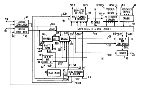
Fig. 2 is a detailed block diagram of a communi-
cation controller 72 constructed according to the teachingsof the invention. Fig. 2 will first be described in its
entirety to provide a complete, overall description of the
invention, before the functional blocks are described in
detail. When elevator controller 32 shown in Fig.
desires to send a serial message to a specific communica-
tion controller 72, which can be a twenty-bit message to
communication controllers associated with FC functions, or
a forty-bit message to communication controllers associated
with PI unctions, the appropriate number of serial clock
pulses CLK are provided on differential pair 68 of the
appropriate data link 64 or 66, while simultaneously
providing a serial message SID of like bit length on
differential pair 70. Receivers 80 and 84 provide a clock
signal CLK and a message signal SID, respectively, at input
terminals having these reference identifications in Fig. 2.
In order to discriminate between line noise and signals CLK
and SID are applied to digital correlators 90 and 92 via
hysteresis inputs (not shown), to block line noise and pass
only valid input signals CCLK and CSID. Digital
correlators 90 and 92 are of like construction, with
digital correlator 90 being shown in detail in Fig. 3.
Serial input message CSID, regardless of bit
length, is clocked into functional block 94 which includes
a shift register and data latches. Function 94 is shown in
detail in Fig. 8.
The parity of the serial message CSID is checked
in a parity checking function 96, which is shown in detail
in Fig. 5. If the parity of the message is correct,
function 96 provides a signal PER at the logic one level.
The number of clock pulses in the serial string
CCLK is counted in a counting function 98. The counting
function is not shown in detail as it is simply provided by
~ 9 53,109
a six-bit digital counter with logic gates connected to
provide a signal C20 which is a logic zero when the count
stops at twenty, and a signal C40 which is a logic zero
when the count stops at 40. The counters do not count
around~ i-e-~ C20 is not low at 40 pulses, nor is C40 low
at 80 pulses.
The parity signal PER from function ~6 and the
clock count signals C20 and C40 from function 98 are
applied to an enable function 100. Enable function 100,
which is shown in detail in Fig. 7, compares its unique
station addres A0-A6 (AO-A4 for PI mode~ with the address
bits in the address field of the message CSID. The station
address A0-A6 is provided by function 102, which may be a
thumb switch. The address bits are bit numbers 1-7 in FC
mod~, and bit numbers 1-5 in PI mode, with the seven
possible address bits appearing at output terminals BlN-B7N
of function 94. The enable function 100 is also responsive
to the level of the voltage of the input pin M. It will be
recalled that pin M is grounded to cause communication
controller 72 to function in PI mode, and it is at the
logic one level for FC mode. The voltage level of pin M
selects input signal C20 in FC mode, and input signal C40
i~ PI mode. Enable function 100 provides a true enable
signal DOUT, i.e., it is at the logic one level, only when
all of the following conditions occur: (l) the address in
the address field of message CSID correctly matches the
station address; (2) the parity of the message CSID is
correct, i.e., sig~al PER is a logic one; and (3) the
correct number of clock pulses CCLK has been received
according to the logic level of input pin M. If pin M is
high, signal C20 must be low, and if pin M is low, signal
C40 must be low.
The various functions of communication controller
72 are properly sequenced and synchronized by a ring
66~2~
53,109
counter and divider function 104, which is shown in detail
in Fig. 6. An oscillator 106, such as may be provided by
an external RC networX, or by a crystal, provides a clock
signal RC which is selected to be substantially greater
than the rate of the message clock CLK, such as 64 times
greater. Clock RC is divided by two to provide clock RC2,
which is used by the digital corre:Lators 90 and 92, and
clock RC is divided to provide a clock RC64 which has the
same nominal rate as the message clock CLK. Clock RC64
clocks the ring counter of functiorl lQ4, with the ring
counter being reset by @ach message clock pulse CCLK.
Thus, the clocking of input message CSID must end and three
clock pulses CCLK must be missing, before ring counter
function 104 provide~ a first true output Q4. Three
missing clock pulses CCLK thus frames a message CSID. The
communication controller 72 can be interrupted, i.e., not
lose the data or frame the message, when the input clock
CLK is held high indefinitely. Adjacent messages CSID must
be separated by at least nine missing clock pulses, to
complete the message processing functions of communication
controller 72. The signal Q4, when true, causes the enable
function 100 to make the address comparison, with signal
DOUT going true when signal Q4 goes true, assuming of
course that a valid message directed to this specific
communication controller 72 has been received.
Sig~al Q5 provided by ring counter function 104
then goes true. If the enable signal DOUT is also true,
true signals Q5 and DOUT are logically combined to cause
the data latches of function 94 to latch the data bits in
the data field of the message CSID being held in ths shift
register of function 94. The data bits are bit numbers
8-l9 of a twenty-bit message, and bit numbers 6-39 of a
forty-bit message.
The data latches of function 94 are connected to
a multiplexer and driver function 108, which is shown in
detail in Fig. 10. Function 108 includes at least fourteen
dedicated outputs OUTO-OUTl3. The data latches of function
6~
~ 11 53,109
34 are also connected to an I/O selection and driver
function 110 which includes terminals IN/OUT 0 through
IN/OUT-X, which function as outputs in PI mode and as
inputs in FC mode. The voltage level of mode pin M per-
forms the I/O selection in function 110.
Function 108 multiplexes the data held in twen-
ty-eight latches to provide fourtee!n outputs when the
communication controller 7Z is in PI mode. In other words,
each of the fourteen outputs OUT0 through OUTl3 provides
time multiplexed data from two data latches. In EC mode,
data held by fourteen latches in function 94 appears at the
fourteen dedicatad outputs OUT0-OUT13.
Signal Q6 now goes true to reset the parity check
function 96 and the clock counter function 98, to prepare
them for the next serial message. Serial Q6 also resets
and prepares a parity bit generator function 112, which is
shown in detail in Fig. 9.
Signal Q7 from function 104 now goes true, which
parallel loads sensed data from dedicated inputs IN0-INX
and driver function 114 into the data bit locations 8-19 of
the shift register function 94.
A true enable signal DOUT enables a tri-state
driver 116 for one output message. Driver 116 receives
serial data SODI from the parity bit generator function 112
and applies it to output terminal SOD. The clocking of the
- next message into shift register function 94 by message
clock pulses CCLK also clocks the serial message previously
prepared in shift register function 94 out of terminal B20.
The message clock CCLK is also used to generate a related
clock signal CCKB which is used in the function of prepar-
ing a parity bit for the outgoing message. Output terminal
Bl9 is also used to keep track of the message parity, so
that a parity bit of the correct logic level may be added
to the LSB of the outgoing message. As hereinbefore
stated, the serial output message SOD is always twenty bits
in length, regardless of the voltage level of the mode
selection pin M, and thus the output message SOD will
6~t~
12 53,109
always be properly clocked out regardless of the bit length
of the incoming message SID.
Fig. 3 is a schematic diagram of a digital
correlator constructed according to the teachings of the
invention, which may be used to provide the digital
correlator functions 90 and 92 shown in Fig. 2. ~ince
digital correlators 90 and 92 are of like construction,
only digital correlator 90 will be described in detail.
Fig. 4 is a graph which will aid in understanding the
operation of digital correlator 90.
Functionally, digital correlator 90 samples the
clock input CLK at a rate which greatly exce~ds the rate of
the message clocking pulses CLK. The last N samples are
saved, and when a predetermined number of saved samples has
a predetermined logic level, the logic level of output CCLK
! changes. Output CCLK stays at the new logic level until
the number of saved samples having the predetermined logic
level drops below the number which caused the output CCLK
to change. Using numbers to describe an exemplary embodi-
ment, digital correlator samples the input clock line CLK
at a rate which i9 thirty-two times the message clocking
rate, with the message sampling rate being controlled by
clock RC2. The logic levels of the last five samples are
saved. When three of the five saved samples are at the
logic one level, output CCLK changes from a logic zero to a
logic one. As long as at least three of the five saved
samples are at the logic one level, output CCLK will stay
at the logic one level. Once the number of saved samples
which are at the logic one level drops below three, output
CCLK switches back to the logic zero level. Thus, a noise
pulse having a duration of two or less sample periods is
ignored. Digital correlator 90 thus acts as a digital
filter, providing a clean output signal CCLK only when the
logis one level at the input of the digital correlator
persists for more than one-hal~ of its ive sample period.
More specifically, the last fi~e samples of the
input CLK are saved in five D~type flip-flops 120, 122,
?g~
13 53,109
124, 126 and 128 which are connected to propagate the logic
level of each sample from flip-flop 120 through flip-flop
128. Flip-flops 120 through 128 are clocked by clock RC2,
which, as hereinbefore stated, is 32 times the rate of the
message clocking pulses CLK.
The Q outputs of flip-flops 120 through 12~ are
inverted by inverter gates 130, 132, 134, 136 and 138,
respectively, and applied to certain inputs of ten
tri--input NAND gates 140, 142, 144, 146, 148, 150, 152,
154, 156 and 158. The output of inverter gate 130 is
connected to inputs of NAND gates 140, 142, 144, 146, 148
and 150. The output of inverter gate 132 is connected to
inputs of NAND gates 142, 144, 150, 152, 156 and 158. The
output of inverter gate 134 is connected to inputs of NAND
gates 140, 146, 150, 154, 156 and 158. The output of
inverter gate 136 is connected to inputs of NAND gates 140,
142, 148, 152, 154 and 156. The output of inverter gate
138 is connected to inputs of NAND gates 144, 146, 148,
152, 154 and 158.
The outputs of NAND gates 140, 142, 144, 146 and
148 are connected to inputs of a NAND gate 160, and the
outputs of NAND gates 150, 152, 154, 156 and 158 are
connected to inputs of a NAND gate 162. The outputs of
NAND gates 160 and 162 are connected to inputs of a NOR
gate 164. The output of NOR gate 164 is connected to the D
input of a D-type flip-10p 166. Flip-flop 166 is clocked
by clock RC2, and the Q outpùt of flip-flop 166 is
connected to output terminal CCLK via an inverter gate 168.
The ten tri-input NAND gates cover all of the
combinations of any three-out-of-five, such that any three
samples at the logic one level will cause the output of one
NAND gate to go low, forcing the output of NAND gate 160 or
the oukput o~ NAND gate 162 high. NOR gate 164 will thus
no longer have two logic zero inputs, and its output goes
low. The Q output of flip-flop 166 thus goes low, which is
inverted to a logic one output at output terminal CCLK.
- ~6q5~72~9
14 53,109
In the example illustrated by the graph of Fig.
4, clock pulse CLK goes high at 169 and the rising edges
170, 172 and 174 of RC2 clock pulses all detect a logic one
level. Thus, after the third such detection, flip flops
120, 122 and 124 all have a logic zero at their Q outputs
which is inverted to a logic one by inverter gates 130, 132
and 134, resp~ctively. This combination drives the output
of NAND gate 150 low, the output of NAND gate 162 high, and
the output of NOR gate 164 low. When flip-flop 166 is
subsequently clocXed by the rising edge 176 of clock RC2,
the Q output of flip-fLop 166 goes low which is inverted to
a true signal CCLK by inverter gate 168. Thus, clock CCLK
goes high at 175.
Output terminal CCLK remains at the logic one
level until the count of samples which are at the logic one
level drops b~low three. When pulse CLK ceases at 177,
rising edges 178, 180 and 182 of clock RC2 load three
samples at the logic zero level into the sample-saving
flip-flops, and all ten tri-input NAND gates output a logic
20 one. Thus, NAND gates 160 and 162 output logic zeros, and
NOR gate 164 outputs a logic one. When flip-flop 166 is
subsequently clocked by rising edge 184 of clock RC2, the Q
output of flip-flop 166 goes high, and the inverter gate
168 outputs a logic zero to terminate the CCLK pulse at
25 186.
It will be notad that while the digital
correlator 90 delays the start 175 o CCLK compared with
the start 169 of CLK, the termination 186 of CCLK also lags
the termination ~77 of CLK, to provide substantially the
same pulse duration.
The parity checking function 96 shown in block
form in Fig. 2 may be performed by the circuit shown in
Fig. 5. For purposes of example, the parity bit is select-
ed to make the total number of logic o~es in an SID message
an odd number. Function 96 includes a D-type flip-flop
190, an exclusive OR (XOR) gate 192, and first and second
6l~72g
53,109
inverter gates 194 and 196. Signal Q6 is applied to the
reset input of flip-flop 190 via the first inverter gate
194, to provide a logic one at the Q output of flip-flop
190, which is inverted to a logic zero by the second
inverter gate 196. Thus, signal PER is low when circuit 96
is reset. Input data CSID is applied to one input of XOR
gate 192, the output of XOR gate 192 is applied to the D
input of flip-flop 190, and the Q output of flip-flop 190
is applied to the remaining input of XOR gate 192. Clock
CCLK is connected to the clock input CK of flip-flop 190.
Logic zeros in message CSID result in XOR gate
192 continuing to output a logic zero and the Q output
remains high until the first logic one in the message is
detected. The first logic one triggers flip-flop 96 and
signal PER goes high to indicate odd parity. The second
logic one results in two like inputs to XOR gate 192 and
CCLK will clock a zero to the Q output, output Q goes high
and signal PER goes low to indicate even parity. The third
logic one again triggers flip-flop 190, and signal PER goes
high to indicate odd parity, etc. Thus, if message CSID
has an odd number of logic ones, output signal PER will be
high, indicating that there is no parity error. If signal
PER is low at the end of message CSID, a transmission error
has occurred.
Ring counter and divider function 104 shown in
block form in Fig. 2, may be provided by the circuit shown
in Fig. 6. Function 104 includes an eight-bit ring counter
199 constructed of eight D-tvpe flip-flops 200, 202, 204,
206, 208, 210, 212 and 214. Clock CCLK is inverted by an
inverter gate 216, and the output of inverter gate 216 is
applied to the reset inputs of the eight flip-flops. Thus,
each clock pulse CCLK resets ring counter 199. When all
eight 1ip-flops are reset, their Q outputs are arranged to
provide a logic one or the D input of the first flip-flop
16 53,109
200 via NAND g~tes 216 and 218 and NOR gate 220. Thus,
when the clock pulses CCLK cease at the end of a message
SID, ring counter 199 propogates the logic one which was
initially applied to flip-flop 200 through the ring
counter.
Clock RC, which is provided by the oscillator
circuit 106 shown in Fig. 2, has a clock rate selected to
be 64 times the message clock rate CLK. Clock RC is
divided by a divider 222, such as a six-bit counter, to
provide an output clock RC2 which is thirty-two times the
rate of clock CLK, and an output clock RC64 which is the
same rate as the message clock CLK. Clock RC64 is connect-
ed to the clock inputs CK of the eight flip-flops via a
gating function 224. Gating function 224 is enabled by a
low signal from the Q output of the last flip-flop 214.
When the logic one is propagated completely through the
ring counter 199 and it reaches the Q output of flip-flop
214, gating function 224 ceases to pass RC64 clock pulses,
and the ring counter remains in this condition until it is
reset by the first clock pulse CCLK of the next message
CSID.
In the operation of ring counter and divider
function 104, each message clock pulse CCLK resets ring
counter 139, maintaining a logic one at the D input of
flip-flop 200, and enabling gating function 224 to pass
- clock pulses RC64. One or two missing clock pulses CCLK
will not start any message processing functions in the
controller, as the first such function is not initiated
until the logic one being propagated through the ring
counter reaches the Q output of the fourth flip-flop 206,
which provides signal Q4. Three missing clock pulses CCLK
thus frame the message CSID and start the message process-
ing functions of the communication controller 72. At least
, nine missing clock pulses CCLK are required in order to
guarantee the message processing functions. After Q4 goes
high, outputs Q5, Q6 and Q7 successively go high and then
low, until the Q output of flip-flop 214 goes high, which
17 53,109
disables the gatin~ function 224 to stop the clocXing of
the ring counter 199 until the next CSID message is clocked
by CCLK pulses.
Ths enable function 100 shown in Fig. 2 may be
performed by the circuit shown in Fig. 7. Enable function
100 includes a digital address comparator 230, an OR gate
231 a multiplexer 232, a flip-flop 234 which is enabled by
a low enable input signal, an AND gate 236, and inverter
gates 238, 240, 242, 244 and 246. Address comparator 230
compares the message address with the station address in
comparator 230', providing a true output signal C1 only
when the address portion BlN-B7N of a message CSID matches
the station address AO-A4. Output Cl is applied to one
input of AND gate 236. Address comparator 230 also com-
pares station address bits A5 and A5 with message bits B6N
and B7N in comparator 230", providing a true output signal
C2 only when they match. Output C2 is applied to one
output of OR gate 231 and the mode pin M is connected to
the other input via inverter gate 242. The output of OR
gate 231 is connected to another input of AND gate 236.
Thus, in PI mode, output C2 is ignored, as only bits
BlN-B5N define the controller address. In FC mode all
seven station address bits AO-A6 must match bits BlN-B7N of
the message address field.
The parity check signal PER provided by function
96 shown in Fig. 2, which is high when no parity error is
detected, is applied to another inpu~ of AND g~te 236.
The outputs C20 and C40 of the counting function
98 shown in Fig. 2, are applied to the A and B inputs of
multiplexer 236 via inverter gates 238 and 240, sespective-
ly. The mode pin M is connected to the "select B" input
SLB via inverter gate 242. The Y output of multiplexer 232
provides the final input to AND gate 236~
Control signal Q4 is applied to the enable input
EN of 1ip-flop 234 via inverter gate 244. The Q output o
7~
18 53,109
flip-flop 234 provides the output signal DOUT via inverter
gate 246.
If the communication controller 72 is in FC mode,
the A input of multiplexer 232 is connected to the Y
output, and if communication controller 72 is in PI mode,
the B input is connected to the Y out.put. If the communi-
cation controller 72 is addressed by the CSID message, and
the message contains the correct number of bits for the
sslected mode, FC or PI, and no parity error is detected,
AND gate 236 will apply a logic one to the D input of
flip-flop 234. Otherwi~e, AND gate 236 provides a logic
zero output. When a message has been framed and control
signal Q4 goes high, flip-flop 234 transfers the logic
level at the D input to the Q output, providing the invert-
ed logic level at the Q output. Thus, if a logic one is
applied to the D input, the Q output of flip-flop 234 will
go low when signal Q4 appears, providing a true enable
signal DOUT. If a logic zero is applied to the D input of
flip-flop 234 at the time signal Q4 goes high, the enable
signal DOUT will remain at the logic æero level.
The shift register and data latch function 94
shown in Fig. 2 may be provided by the circuit shown in
Fig. 8. Function 94 includes a forty-bit shift register
250 and a thirty-four bit data latch 252. Shift register
250 includes a serial input connected to the LSB of shift
register 250 to receive either a twenty-bit or a forty-bit
input message CSID. A serial output B19 is provided at the
twentieth bit position, a serial output B20 is provided at
the twenty-first bit position, parallel load inputs are
provided at bit positions 8-19, parallel address outputs
BlN-B7N are provided from bit positions 1-7, and parallel
outputs are provided from bit positions 6-39. The parallel
shift register outputs from bit positions 6-39 are applied
to inputs of the thirty-four bit data latch 252. In FC
mode, only bit positions 8-19 contain data. In PI mode,
bit positions 6-39 contain data.
19 53,109
Enable signal DOUT and control signal QS are
logically combined by NAND gate 254 and an inverter gate
256 to provide a signal which is connected to the latch
input of data latch 252. If the enable signal DOUT is
5true, when control sigrlal Q5 goes to a logic one, a logic
one is applied to latch 252 which latches the data applied
to its inputs.
Control signal Q7, which goes to a logic one
after the data in message CSID has been latched, loads bit
lOpositions 8-19 with data from the sensed inputs INO-INX.
INX is INll for FC mode and IN3 for PI mode. Thus, a new
message is then ready to be clocked out when the next
message CSID is clocked into shift register 250. The
address appearing in bit positions BlN-B7N is undisturbed,
15as it is the address of the communication controller 72
which is sending the message SOD back to the elevator
controller 32. The logic level of the LSB of message SOD
is provided by the parity bit generator 112. Clock CCLK is
delayed via a gating function 258 to provide delayed clock
20CCKB which is used to clock a flip-flop which checks the
parity of each new bit appearing in bit position B19 of
shift register 250, slightly after the message clock CCLK
advances the shift register.
The parity generator function 112 shown in Fig.
252, may be provided by the circuit shown in Fig. 9. The
parity generator function 112 includes a D-type flip-flop
260, an "enable" flip-flop 262, a mult:iplexer 264, an
exclusive OR (XOR) gate 266, an exclusive NOR (XNOR) gate
268, and inverter gates 270 and 272. Control signal Q6
30resets flip-flops 260 and 262 via an inverter gate 270.
Flip-flop 260 and XOR gate 266 keep track of the nurnber of
bits in the output message as it is being clocked out, in a
manner which is similar to the parity check function 96
shown in Fig. 5, with the Q output of flip-flop 260 being a
35logic zero when the number of logic one bits is even, and a
logic one when the number of logic one bits in the message
is odd. The Q output of flip-flop 260 is applied to one
3",~d66~729
53,109
input of XNOR gate 268, and the output of XNOR gate 268 is
applied to the A input of multiplexer 264.
Output C20 from the counting function 98 shown in
Fig. 2 is applied to the enable input EN of flip-flop 262.
Thus, flip-flop 262 is enabled to pass SOD message bits
from serial output B20 of shift register 250 to its Q
output until signal C20 goes low at the twentieth clock
pulse CCLK. ~fter the twentieth clock pulse CCLK, only
nineteen message bits have been clocked out of terminal
B20. When signal C20 goes low, flip-flop 262 provides a
logic zero to input of XNOR gate 268. Th~ Q output of
flip-flop 262 is also applied to the B input of multiplexer
264. Clock counter output C20 is applied to the select
input of multiplexer 264. The initially high signal C20
selects input B, allowing ninekeen SOD message bits to pass
through multiplexer 264 to ~erial output terminal SODI.
When signal C20 goes low after twenty clock pulses CCLK,
multiplexer 264 connects its A input to the output terminal
SODI. The delayed twentieth clock pulse CCKB clocks
flip-flop 260, providing a zero at th input of XNOR gate
268 if the message contained an even number of logic one
bits. The output of XNOR gate 268 with two logic zero
inputs goes to a logic one which thus becomes the LSB of
the twenty-bit output message SOD. Elip ~lop 260 provides
a logic one at the input of XNOR gate 268 if the message
being clocked contained an odd number of logic one bits.
~he output of XNOR gate 268 with different logic level
inputs goes to a logic zero, which thus becomes th~ LSB or
parity bit of the twenty-bit output message SOD. Thus, add
parity for the twenty-bit SOD message is always
transmitted.
As shown in Fig. 2, serial output message SODI
passes through the tri-state driver 116 to output terminal
SOD, since the enable signal DOUT is maintained at the
logic one level until the next message is framed.
67~g
21 53,109
The multiplexer and driver function 108 shown in
Fig. 2 may be provided by the circuit shown in Fig. 10.
Fig. 11 is a graph which will also be referred to while
describing function 108. Function 108 includes fourteen
multiplexers, with the first being referenced 280 and the
fourteenth 282. Each multiplexer has its A and B inputs
conneçted to the output of different data latch elements of
latch 252 shown in Fig. 8. The Y outputs of the fourteen
multiplexers are connected to the dedicated output termi-
nals OUT0-OUTll, and to terminals OUTl2 and OUT13, which
are outputs in P~ mode, via drivers, such as drivers 284
and 286. The "select" inputs S of the fourteen multiplex-
ers are connected to be responsive to the mode pin M and
clock RC64 via inverter gates 288, 290, 292 and 294, and a
NAND gate 296. Mode pin M is connected to an input of NAND
gate 296 via inverter gate 288, clock RC64 is connected to
the remaining input of NAND gate 296 via serially connected
inverter gates 290 and 292, and the output of NAND gate 296
is applied to the select inputs S of the fourteen multi-
plexers via inverter gate 294.
In FC mode, pin M is high and NAND gate 296
outputs a logic one which is inverted to a logic zero by
inverter gate 294. A logic zero selects the A inputs to be
connected to the Y outputs.
In PI mode, pin M is low which enables NAND gate
296 to pass clock RC64. Thus, the Y outputs of the four-
teen multiplexers are switched between the A and B inputs
at the rate of clock RC64. In PI mode, the A inputs of the
fourteen multiplsxers control the fourteen segments of the
least significant (LS) digit 298, and the B inputs of the
fourteen multiplexers control the fourteen se~ments of the
most significant (MS) digit 300. Digits 298 and 300
collectively form the digital car position indicator 302.
Eunction 108 further includes a D-type flip-flop
304, NAND gates 306 and 308, and inverter gates 310 and
312. Clock RC is applied to the clock input CK of
flip-flop 304, and clock RC64 is applied to the D input of
22 53,109
flip-flop 304 and to an input of NAND gate 306. The Q
output of flip-flop 304 i5 applied to the remaining input
of NAND gate 306. The Q output of flip-flop 304 is applied
to an input of NAND gate 308, and clock RC64 is applied to
the remaining input of NAND gate 308. The output of NAND
gate 306 is inverted by inverter gate 310 to provide an
output signal CATA which is connected to the cathode of the
LS digit 298. The output of NAND gate 308 is inverted by
inverter gate 312 to provide an output signal CATB which is
connected to the cathode of the MS digit 300.
As illustrated in Fig. 11, output signals CATA
and CATB function as non-overlapping clock signals which
energize their associated digit of the digital car position
indicator while the ~ourteen dedicated outputs are provid-
ing segment information for that digit. The rate isselected to be greater than the persistence of the human
eye, causing each digit of the car position indicator 302
to appear to be continuously energized.
Fig. 1 illustrates a typical use for the latched
data which appears at the dedicated outputs OUTO-OUTll in
an FC input message SID, and it also illustrates typical
sensed data which may be packed into the output message
SOD. The sensed data is applied to the dedicated inputs
INO-INX shown in Fig. 2. As illustrated in Fig. 1, the
down hall call pushbutton S6 is connected in a serial
circuit which starts ~rom a source 320 of unidirectional
potential, and continues through a resistor 322 and push-
button 56 to ground. Indicator lamp 58, which is associat-
ed with pushbutton 56, is connected from source 320 to
ground via serially connected resistors 324 and 326, with
lamp 58 and resistor 322 being connected in parallel at
junction 330. A solid state switching device, such as a
field effect transistor 328, has its drain D connected to
thP junction 330, its source S connected to ground, and its
gate G connected to receive one of the outputs OUTO-OUTll.
The junction 332 between resistors 32~ and 326 is used to
23 53,109
sense actuation of pushbutton 56, with junctlon 332 being
connected to one of the dedicated inputs INO-INX.
Normally, a voltage appears at junction 332 of
the voltage divider which includes resistors 322, 324 and
326. When pushbutton 56 is actuated, junction 330 is
colmected to ground, and the voltage at junction 332 drops
to ground level. When the associated input is at ground
potential, this fact is sensed and sent back to the eleva-
tor controller 32 as part of serial message SOD. The
elevator controller 32 receives the hall call indication
and acknowledges receipt thereof by sending a message SID
to the associated communication controller 72, with a logic
one being provided in the data location of the m0ssage
which will be latched to provide gate drive for the solid
state switch 328. When switch 328 turns on, lamp 58 is
energized. When the hall call is answered, a message SID
will be prepared by the elevator controller 32 and sent to
this communication controller 72, with this messaye con-
taining a logic zero at the location which will remove gate
drive from switch 328 and turn lamp 58 off.
In summary, there has been disclosed a new and
improved versatile communication controller for elevator
communication control which may be used either for floor
controller functions or car position indicator functions,
simply by controlling the logic level of a single input
pin. This single input pin M is internally connected to a
logic one voltage level with a pull-up resistor, requiring
only that pin M be grounded when the communication control-
ler is to be used in PI moda. Grounding pin M automatical-
ly enables the communication controller to accept forty-bit
messages, instead of twenty bit messages, it automatically
activates a multiplexing function such that two
fourteen-segment digits can use fourteen outputs of the
controller, and it automatically converts certain of the
communication controller terminals which are inputs in FC
mode to output terminals. Communication controller 72 also
effectively guards against erratic operation due to noise
i7Z~
24 53,109
in the data link by digitally correlating the clock and
input message signals via digital correlators which ignore
line noise and provide clean digital signals in response to
actual signals received on the clock and input message
lines. Communication controller 72 further guards against
erratic operation by requiring at least three missing
message clock pulses to trigger message framing. Thus, one
or two missing clock pulses will not start message process-
ing functions in the communication controller.
Once internal message processing starts, the
processing steps are sequenced and synchronized by a ring
counter which is effectively under the control of the
message clock line CLK provided by the elevator controller
32. For example, each message clock pulse CCLK resets the
ring counter, requiring three missing clock pulses to frame
the messaqe, and at least nine missin~ clock pulses are
required in order to complete message processing.
The communication controllers operate in a full
duplex mode with the elevator bank controller, as the
clocking of an input message SID loads the message into the
shift registers of all communication controllers, regard-
less of whether the communication controller is in FC or PI
mode. The clocking in of a message simultaneously clocks
out a message SOD from the communication controller which
was addressed by the preceding message. In other words,
information is sent from a communication controller to the
elevator bank controller when it's return data interface,
i.e., the tri-state driver, is enabled. This interface is
enabled for one message following the reception of a valid
received message from the elevator bank controller. Thus,
a message transmission from the elevator bank controller to
one particular address controll~r results in the simulta-
neous reception of information from the previously ad-
dressed communication controller.
Reception of a valid message is insured by each
communication controller, even though the elevator bank
controller interleaves different length SID messages, by
53,109
circuitry which counts the number of bits in each SID
message. A mode pin M dstermines if the correct count
should be twenty or forty. If this correct clock count is
not achieved, the message is ignored. The parity of each
incoming message is also checked. IE it is not correct,
the message is ignored. The address in the address field
of the SID message is compared with the unique station
address assigned to each communication controller. If the
addres~es do not match, the message is ignored.
10All return messages SOD have a twenty-bit length.
Thus, all return messages are clocked by an in-coming
! message regardless of whether the in-coming message has
twenty bits or forty bits. The return message is prepared
in the shift register of a communication controller which
lS just received a valid SID message, by retaining the address
in the addres~ field of the SID message, and by parallel
loading the data field with sensed data, after the data in
the SID message has been latched. A parity bit is added by
a parity generator, as the SOD message is clocked out.