Note: Descriptions are shown in the official language in which they were submitted.
IN THE UNITED STATES PATENT AND TRADEMARK OFFICE
AP P L I CAT I ON FOR PAT ENT
SELECTIVE OPERATION OF PROCESSING
ELEMENTS IN A SINGI.E INSTRUCTION,
MULTIPLE_DATA _TREAM t S MD ) COMPUTER SYSTEM
Inventors: Adam E. Levinthal
Thomas K. Porter
Thomas D.S. Duff
Loren C. Carpenter
Background of the Invention
This invention relates generally ~o parallel
data processing techniques and computer systems, and
specifically to those of a type where each of a plurality
of parallel processors simultaneously executes the same
instruction on different data. 5uch a computer is
commonly termed a single instruction, multiple data
stream (SIMD~ processor.
There are many data processing applications
wherein multiple streams of data may be processed in the
same manner. An example is in the field of computer
graphics where separate video red, green, ~lue and alpha
digital signals may be processed identically~ To achieve
the highest processing rate, it is thus convenient to
process these four data streams simultaneously with the
same sequence of instructions. That is, at any given
instant, separate red, green, blue~and alpha data for a
particular color display pixel are being simultaneously
processed.
~; ~ Parallel processing is particularly fast if the
program being executed on the parallel streams of data is
,
,
:: ~".,
, . . . ~, ~ . , , , ~ - . . .
,. :. ..
- . -
., , , ,~. ,
~,
,,,: :,
, ." .
: . - :,
:.,: ~ ;
- ~ ~ : , , . : '
'7~3~3
,
an invariant series of statements. It is more common,
however, that the con~rolling program includes condi-
tional statements that depend for execution upon the da~a
in each of the parallel processors. Since the data being
processed in each stream will be different, provision
must be made in this case for those processors whose data
does not meet the condition of the program statement to be
rendered non-operative during the time that the remaining
processors are executïng the particular statement. It is
known that a WHILE-DO construct is the minimum needed to
implement all possible flow control structures.
A common example of such a conditional program
instruction is an "IF-THEN" statement: that is, the
individual processors are all instructed to perform a
certain manipulation of their individual data streams,
but only "if" their data meets a certain condition
expressed in the program instruction. Those processors
whose data at that instant do not meet the condition do
not execute that in~truction. An "IF-THEN" instruction
is o~ten augmented by an "ELSE" modifier; that is, those
processors not executing the "I~-THEN" statement are
subsequently instructed to execute a different operation
on their data at the next instant while those processors
who did execute the "IF-THEN" instruction are rendered
inoperative.
It is a general object of the present invention
to provide improved techniques and circuits for selec-
tively controlling which of a plurality of parallel
processors execute speci~ic conditional instructions.
Summary of the Invention
This and additional objects are accomplished by
the present invention, whereinl briefly, each of ~he
~,
,. ~ ` ..'
" ~
3 ~ t3~
parallel processors has a separate control element, such
as one bit of a control register, that enables the
processor to execute a common instruction given all
processors when the element is in one state and disables
the processor from e~ecuting that instruction when in its
other state. The state of each control element is set to
control execution of a particular statement dependent
upon whether the data for that processor met the test of a
previous instruction, such as an "IF-TH~N" instruction.
In subsequent complementary execution, such as occurs in
an "ELSE" instruction, the states of the control elements
are reversed so that those processors who did not execute
the first statement will execute the subsequent state-
ment, and vice versa.
In addition, in order to provide a capability
for nested excecution of such complementary types of
instructions, a memory device (a stack memory in a
preferred embodiment) is provided to s~ore the states of
the individual control elements when the nested condi-
tional statement occ~rs. When execution of the nes~ed
instruction is completed, the states of the control
elements at the time of the nesting conditional statement
are restored so that the processing of them may continueO
Additional objects, features and advantages of
the various aspects of the present invention will best be
appreciated from a description of its preferred embodi-
ments, which description should be taken in conjunction
with the accompanying drawings.
Brief Description of the Drawin~s
Figure 1 illustrates in general block diagram
form a SIMD processor;
Figure 2 illustrates a first circuit embodiment
- ...
, ' .:
' ~ ' : :. ~ : :
.
4 ~ti'7~
of the control circuits of the system of Figure l;
Figures 3 and 4 are tables which illustrate the
operation of the system of Figure 1 when implemented with
the control circuit of Figure 2;
Figure 5 illustrates a second circuit embodi-
ment of the control circuits of the system of Figure l;
Figures 6 and 7 are tables which illustrate the
operation of the system o~ Figure 1 whem implemented with
the control circuit of Figure 5; and
Figure 8 provides logic details of another
portion of the circuit of Figure 1.
Description of the ?referred Embodlments
Referring to Figure l, the overall architecture
of a computer system utilizing the various aspects of the
present invention will be described. Separate pro-
cessors 11, 13, 15 and 17 receive, respectively, inde-
pendent data streams in input lines 19, 21, 23, and 25.
5imilarly, independent lines 27, 29~ 31, and 33 carry~
respectively, the outputs of the processing elements.
Four parallel data processors are illustrated in this
example, but it will be understood that the principles of
the present invention apply to a parallei system contain-
ing arbitrarily many parallel processing elements. Four
processors are conveniently used in a graphics computer
system, one channel used to process data of the red
component of a video signal, another for the green
component, a third for the blue, and a fourth for an alpha
component that provides other information of the image.
Parallel proce~sing is particularly adapted for a gra-
phics application since high speed processing is a
requirement and the same sequence of program instructions
is executed simultaneously on all four data paths.
, -
.
,
:. :
, :
: ~ ~ ~. '' ': ` ' ' '
: ` .,
.. . .:
, ::: :, . ,:
There are certain program instructions, how-
ever, that require one or more processing elements to not
participate in executing a particular program instruction
that is applied simultaneously through an instruction bus
35 to all four of the processing elements 11, 13, 15 and
17 In order ~o control which of the four processing
elemen~s are active to execute a particular instruction,
a control circuit is provided in association with each of
them, such as a circuit 37 which controls operation of the
processing element 11. A line 39 carries a signal to the
processing element 11 which controls whether it is
enabled to execute an instruction on the bus 35. Por
example, a voltage in line 39 representative of a logical
"1" will cause the processing element to execute the
in~etrUction~ while a voltage representative of a logical
"0" will disable the processing element during execution
of that par~icular instruction by other of the processing
elements.
Each of the four control circuits of the system
of Figure 1, such as tbe circuit 37, determines whether to
enable its associated processing element, such as pro-
cessor 11, on the basis of several pieces of in~ormation.
One is an initial condition which is presented external of
the circuits of Figure 1 in a set line 41. Another piece
of information is a status instruction in a bus 43 which
specifies, for those processor instructions on bus 35
that may require less than all of the proce~sing elements
to execute the instruction, additional instructions for
determining the state of the enable signal in the line 39.
A final piece of information is a true "1" or false "oe'
signal in a line 45 which gîves the result of a test
performed by the processing element 11 on its data in
response to a current or immediately preceding instruc-
~,... . .
. . '':: - .
. ~ :
..
: .
:. .
: ~ :
d ~ ~O
tion on the bus 35. Each of the four control circuits
shown in Figure 1 operates similarly, except that the test
result input received from its associated processing
element can be different and thus result in some
5 processors being enabled and others being disabled at a
given in~tant in time.
The ~unction of the control circuits in the
system of Figure l is explained more fully with respect to
its two preferred embodiments, one embodiment illustrated
in Figures 2-4 and another in Figures 5-7. But before
proceeding to those embodiments, some general items of
the system of Figure 1 are first explained. The pro-
cessor instructions in the bus 35 and the status
instructions 43 originate from a micro-programmed control
unit such as micro-sequencer 47. A micro-programmed
control unit consists of the micro~program memory and the
structure required to determine the address of the next
microinstruction, specific implementations being well
known.
A logic circuit 49 has as inputs the invidiual
test result lines of each of the processing elements.
The logic circuit 49 generates a condition code in an
output line Sl when the signals in the input test result
lines are a particular one or more combinations. The
signal in the line 51 is connected to the condition code
input of the micro-sequencer 47, thus enabling a change in
the sequence of instructions in response to a particular
combination of test result outputs. Another input to the
logic circuits 49 is by way of a line 53, an instruction
field of the micro-sequencer ~7.
In a particular implementation of the system of
Figure l for color computer graphics processing, each of
the processing elem~nts contains as prim~ry components a
..
. .
-
:~ , ". ~ . .
7 ~ 3~3
16-bit multiplier and a 16-bit arithmetic and logic unit
(ALU). Extremely fast processing is desired in computer
graphics applications because o~ the large number of
pixels in each ~rame o~ a picture, each pixel being
defined by four 16-bit words.
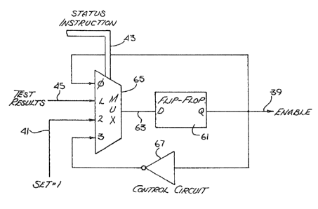
Referring to Figure 2, a circuit is shown that
is suitable for use, according to one embodiment, as each
of the control circuits shown in Figure 1, such as the
circuit 37. A ~lip-flop circuit 61 has its output
connected to the enable line 39. An input line 63 is
connected to an output of a four-position multiplexer 65.
The multiplexer 65 has four separate inputs 0-3. The
status instruction in the bus 43 selects which of the
inputs 0-3 is connected to the output 63. The 0 input of
the multiplexer is connected directly to the output of the
flip-flop 61, thereby allowing the current state of the
flip-flop 61 to be held when the multiplexer 65 is
switched to its 0 input. Conversely, when switched to
i~s number 3 input, the state of the flip-flop 61 is
changed since its output is connected through an inverter
67 back to its input. The number 1 and number 2 position
input positions of the multiplexar 65 are the test result
line 45 and the set line 41, respectively, previously
discussed with respect to Figure 1.
The specific circuit examples being described
: are particularly adapted for ex~cuting IF-THEN-ELSE
program instructions. The table of Figure 3 sum~arizes
the four possible states of the control circuit of Figure
2-, depending upon the status instruction on the bus 43.
: 30 When the multiplexer 65 is switched to its 0 input, the
output in the line 39 is held, the condition desired when
: ~ the logical operation commanded by the instruction on the
~: bus 35 of Figure 1 is to execute a statement. The next
,,
: ~ . : , ..
~ . . .: ,~ , , . . : ; , .
- : , :: .
.. , -::
~. , -
", ~
.
status instruction, selecting the l input of the multi-
plexer 65, causes the test result of its associated
processing element to be stored, as previously described,
an operation that accompanies an IF instruction in the bus
35. The status instruction 2 causes the flip-flop 61 to
be set, a status instruction o~ bus 43 tha~ accompanies an
END IF instruction in the processing element instruction
bus 35. Lastly, a status ins~ruction 3 causes the flip-
flop element 61 to chanqe state in order to enable those
processors previously disabled, and conversely to disable
those processors previously enabled. The status in-
struction 3 is presented in the bus 43 simultaneou~ly with
the ELSE instruction in the bus 35. Micro-code in the
micro-sequencer 47 assures that the instructions in the
buses 35 and 43 correspond according to the table of
Figure 3 in accordance with other particular requirements
of any application.
The table of Figure 4 better explains the
operation of the circuit of Figure l, when using a control
circuit of Figure 2, by a speciic example. Consider the
example of an IF statement asking whether the data input
to each processing element (DI) is greater than l. As
shown in line 2 of the table of Figure 4, it is assumed in
the "test result" column that the first and third
processing elements have passed the test, thus showing
the logical "l" in their test result output lines 45,
while the second and fourth processors have failed tbe
test, and thus show a test result logical signal of "0".
Even though each processor is executing the same IF
instru~tion, the results of the test performed by each can
be different because the data being processed by each is
generally differentO
At the same ~ime the IF instruction is being
:
: : :
.
,
. . .
.:.
~ : ,, , .. , -- .
executed, the status instruction on the bus 43 causes the
multiplexer 65 of each of the control circuits of the
system of Figure 1 to switch to its position 1 to receive
the test results from their corresponding processors.
These test results, whether a test pass "1" or fail "0~,
are then stored in the individual flip-flop elements.
The enable signal outputs of the four flip-flops are given
as the enable signals in the table of Figure 4, referred
to interchangably in this example as "run flags". At
line 2 of the table of Figure 4, the runflags are causing
those processing elements who pass the te~t to be enabled
and those who did not to be disabled. Those which are
enabled are then caused, as shown in the line 3 of the
table of Figure 4, to execute a statement, in this example
chosen to be to set the data output (Do) equal to 1 of the
enabled processing elements. The disabled processing
elements do nothing at this time.
An ELSE instruction is next presented to all
the processing elements for execution, which is to say
that those processors who failed the IF test are now going
to be called upon to do something different, as illus-
trated in lines 4 and 5 of the table of Figure 4. The ELSE
processor instruction is accompanied by the status
instruction 3 which causes the control circuits, illus-
trated in Figure ~, to all invert the states of theirflip-flops. That can ~e seen hy comparing the run flags
of lines 3 and 4 of Figure 4, one being the complement of
the other. Once the processors previously disabled are
enabled, a statement is executed, as shown in line 5 of
Figure 4, wherein in this example the output data value is
set equaI to the input data value. The re~ult of the
routine illustrated in Figure 4 is thus to set the value
of the data output lines 27 and 31 equal to 1, and output
: ~ '
.. ..
,. ~ .
~ 3v
lines 29 and 33 equal to the value of the corresponding
data input. Complementary operation of the processors to
execute the IF and ELSE instructions is made possible by a
simple provision in each of the control circuits for
inverting all of their states in response to a single
status instruction.
Th~ logic circuits 49 of Figure 1 are useful for
detecting conditions where, because of a particular
combination of input data, certain instructions need not
be executed. In sucb a case, the micro-sequencer 47 is
then caused to skip the unexecutable instructions. Logic
circuits 49 may be omitted in implementations where
unexecuted instruction sequences may be allowed to occur.
In the example of Figure 4, if the test results shown in
line 2 had all been 0, then there is no need to execute the
statement of line 3 since all processors would be
disab7ed. For this particular example, therefore, the
logic circuits 49 are designed to detect when all
processor test results are false (0) and causes ~he
condition code in the line 51 to change, with the
resultant change of the instruction sequence issued by
the micro-sequencer 47. Additionally, if the test re-
sults are all true (1), then the instructions at lines 4
~nd 5 of Figure 4 do not need to be executed, so the
condition code in the line 51 can cause that instruction
sequence to be bypassed, as well. A signal in line 53
functions to allow testing for any false (0) condition or
any true (1) condition. Thu~, the ability is provided
(in conjunction with the status instruction on the bus 43)
for testing for any or all conditions true or false.
An example of specific logic for carrying out
these functions i~ given in Figure 8. An OR gate 52 has
as its inputs the test result lines from all of the
:.- .:, :
. , ,
: ,.
,
1 1
processing elements. The gate's output is one input of
an exclusive OR gate 54, the select line 53 being the
second input~ The output of the gate 54 is the condition
code line 51. The ~ate 54 opera~es to pass through the
output of the gate 52 when the select line 53 is false (0),
and to pass a complement of that output when the line 53 is
true (1).
Certain applications will require the ability
of the individual processing element control circuits to
handle a set of instructions that is nested within an IF-
THEN-ELSE series of instructions. When this is required,
the run flags determined as the result of executing the IF
instruction are stored while the nested set of instruc-
tions is being executed. Once the nested instructions
have been executed, the stored run flags are called out of
memory so that the remainder of the IF-THEN-ELSE set of
instructions can be executed.
The control circuit of Figure 5 allows such
-nested program instruc~ion operation. Added to the
system circuit of Figure 1 is a stacked memory 81, and
associated controlling decoder circuits 83~ The cir-
cuits within the dotted outline of Figure 5 are not
repeated within each of the four control circuits of
Figure 1, but rather are shared by themO The decoding
circuits 83 respond to status instruc~ions in the bus 43
to cause the current enable signals (run flags) of each of
the control circuits to be stored in the stack memory 81
(a "push") through lines 8~ or to be read from memory (a
"pop'l) through lines 87. As is well known, stack
memories read t"PoP") the last written (1'pushed") data.
And each time data is written when there already is data
in the stack memory, the existing data is pushed to a
lower level in a manner that it can be read out of the
:
. ~
.~.
,, ' ~' . :~:
.
12 ~ ~ ~ 7
memory only af ter the mos~ recently written data is read
outc In other words, data is read out in a first-in,
last-out sequence.
Returning to Fi~ure 5, the circuitry of each of
the four control ~ircuits of Figure 1 is described for
this embodiment. A flip-fl~p 91 of the same type used in
the embodiment of Figure 2 is employed, with this output
being the enable signal, one bit of the four-bit run flag~
Its input in a line 93 is also connected to an output of a
multiplexer 95. The multiplexer, however, has five
positions 0-4, one more than used in the embodiment of
Figure 2. One of these inputs is selected at a time for
connection to the inpu~ of the flip-flop 91 by the status
instruction in the bus 43. The O input is connected
directly to the flip-flop output, thus serving to hold the
flip-10p in whatever state it is found when switched to
that position~ Input 1 of the multiplexer receives the
output of AND gate 97, having as one input the output of
the flip-flop 91 and as the other input test result line
45 of its associated processorO As indicated in the
table of Figure 6, the status instruction 1 is also
decoded by circuits 83 to store (npush"~ at the top of the
stack memory 81 the output (run flags) of the flip-flops
within the control circuits of Figure 1.
Multiplexer input 2 is connected to the set
line 41. Input number 3 is connected to the stack memory
81 for setting the flip-flops in accordance with what has
previously been recorded at the top of the stack. The
decoding circuits 83 cause the top stack data of the
memory 81 to pop when the status instruction 3 is
received.
The last input of the multiplexer 95, switched
in response to a status instruction number 4, receives the
, - . : .
::
:: ' ' !: ' `: ~ ' : '
. .
~j'7
13
output of another AND gate 99 whose two inputs are
connected to the stack memory output and the output of the
flip-flop 91 through an inverter 101. The result is to
AND together the data stored at the top of the stack and a
complement of the current run flag~. -
The control circuit of Figure 5, whose logical
operation is shown in the table of Figure 6, is especially
adapted for carrying out the sequence of operations given
in Figure 7. In that sequence, an IF-T~EN-ELSE sequence
of program instructions is executed at lines 1, 2, 3, 9,
10, 11, 17, 18, and 19. Nested inside the IF or EL5E
portions of that set o~ instructions is ye~ another IF-
THEN-ELSE series of instructions, at lines 4-8.
Similarly, a second set of such stat~ments is nested at
lines 12-16 within the basic sequence of instructions.
In each of the three IF-THEN-ELSE series of instructions,
a different test result is assumed, as shown in the "test
result" column of Figure 7. These dllifferent test results
cause different run flags for each of the three IF-THEN-
ELSE series of instructions. The dotted arrows show the
flow of run flag bits in the course of the operation of the
stack memory 81, those arrows pointing generally to the
right being the result of a push operation and those
generally to the left the result of a pop operation.
Although the various aspects of the present
invention have been described with respect to its
preerred embodiments, it will be understood that this
invention is entitled to protection within the full scope
of the appended claims.
,
~ ` : - : :
, .
~ '' :~. ~ ;'
. : ,: ~
. . ~ . .
-