Note: Descriptions are shown in the official language in which they were submitted.
~2~74~i~
OPTICAL DEVICE PACKAGE:
1 Field of ~he Invention:
The present invention relates to optical devices such
as light-emitting diodes and photodiodes, a method for
producing them, and packages for such o~tical ~evices.
Background of the Invention:
.
In an optical;devi¢e such as a light emitting device
or a light receiving device, and a package for such optical
~; device, there have been the following technological
requirements:
(a) It must have a light introducing structure which is
transparent to~light;
(b) It must be~wlred as by die~bonding or wire bonding to
lead electrode terminals out of it;
(c) It's chip must be sealed off hermetically; and
(d) It must have a~high coupling efficiency with an opti-
~` cal fiber. That is, a light emitting diode chip or a photo-
diode chip must be~sufficiently close to the~optical fiber
in~end faces and must have a large opèning angle. Further,
the chip must have a~c;lean light receiving surface which~is~
0 not stained with paste or like material.
, ~ ~
Brief Descr-iption of the Drawlnqs:
Fig~ l is a sectionàl view of a conventional upper
surface~type package for optical device, having a glass
window in the upper surface;
~t~ 25 ~; Fig.~2~is~a`sectional view of a: conventional upper
` sur~ace type~package for optical device, having a sapphire
window in the upper surface;
Figs.~3 to~S are sectional views of conventlonal
~ lower surface through hole type packages for optical device;`~ 30 Fig. 6 is an enlarged sectional view for illustration
; of the range of light incident to the light receiving por-
tion of the conventional lower surface through hole type
optiaal device;
''. `~1 ;~ ~:
~ ~;., ~
,~
- :
. ~ ` ' , '
1 Fig~ 7 is an enlar<!ed sectional view for illus~ration
of the ranye of light inc;,clent to the light receivinc~ por-
tion of the conventional lower surface khrouglA hole ~7pe
optical device in the case where the optical deyice chip is
mounted off the predeterm;lled position;
Fig~ i3 is a plan view of a package for optical device
of a sapphire substrate with a co~er removed;
Fig. 9 is a sectional view taken along the line IX-IX
of Fig. 8;
Fig. 10 is a sectional view of the optical device in
which the optical device chip is die-bonded to the package
of ~ig~ 9;
Fig,. 11 is an enlarged plan view of an essential
portion of the die bonding pad shown in Figs. 8 and ~,
Fig. 12 is a sectional view taken along the line
XII-XII of Eig. 11;
Fig. 13 is a sectional view showing the state :in
which gold paste is screen printed on a sapphire substrate;
Fig. 14 is a sectional view showing the state,of the
sapphire substrate with the gold paste thereon burned in a
furnace;
- Fig. :15 is a sectional view showing the state in
which an optical device chip is placed on the gold pa~te;
Fig. 16 is a sectional view o~ an example of a con-
ventional mesa type photodiode chip;
Fig. 17 is a sectional view showing the state :inwhich a bonding pad is formed on a ceramic su~strate having
a light introducing hole therethrough;
Fig. 18 is a sectional view showing the state in
which a ring solder is mounted on the bonding pad of F:ig. 17;
; Fig. 19 is a sectional view showing the state in
which a photodiode chip is placed on the ring solder oE
Fig. 18 and soldered thereto;
~6~
-- 3 --
1 Fig . 20 is a sectional view showing the state :in
which the ring solder is mounted off the predetermined posi-
tion on the bonding pad of Fig. 17;
Fig. 21 is a sectional view showing the state in
which a photodiode chip is placed on the ring ~older of
Fig. 20 and soldered thereto;
Fig. 22 is a sectional view of a sapphire substrate;
Fiy. 23 is a sectional view showing the state .in
which the sapphire substrate of Fig. 22 is provided with a
tapered portion and a concavity;
Fig. 24 is a sectional view showing the state in
- which gold paste is screen-printed on the sapphire substrate
in such a manner that ends of the gold paste are positioned
on the tapered portion of the substrate;
Fig. 25 is a sectional view showing the state in
which the sapphire substrate and the gold paste have been
burned;
Fig. 26 is a sectional view illustrative of the
relationship between the light receiving portion and the
opening angle of the optical device chip disposed in the
package according to the present invention;
- Fig. 27 is a sectional view of an example of a mesa
type photodiode according to the present invention;
Fig. 28 is a sectional view showing ~he state :in
which the mesa type photodiode chip of Fig. 27 is disposed
on the sapphire substrate package for optical device; and
Fig. 29 is a sectional view showing the state in
which the mesa type photodiode chip of ~ig. 27 is disposed
on the ceramic substrate package for optical device.
'
~,r, ~ ,
. ~
~ ~ 6'7~g~
1 The present invention intendt; to answer particularly
the requirement (d) above.
Prior Art I Upper Surface Type
Fig. 1 is a sectional view of a prior art package
for a photodiode. This package is ~ most common type in
which light o~ an optical fiber is incident t~ ~t through
the upper surface of it. In Fig. 1, a TO18 type package 1
comprises a package body 2 and a cap 3 to cover the,upper
surface of the body 2. The cap 3 has an opening at the
center of the top thereof, which has a transparent kovar
glass therein to serve as a window 4~ A photo diode chip
5 is ~ie-bonded to the top plate of ~,he package body 2.
The top plate of the package body 2 is provided with a lead
6. Another lead 7 and an electrode on the photodiode chip
5 are wire-bonded with each other by a gold wire 8. An
optical fiber 9 is disposed ~u~side of the window 4 in
opposition to the photodiode chip 5.
The cap 3 and the body 2 are welded together on sides
thereof. This package is of a hermetic seal type which has
been bringing satisfactory results for a long tim~. In this
package, since light is incident to it from the upper sur-
face where the wire bonding (~old wire,8) exists, the dis-
' tance between the upper surface of the photodiode chip 5
and the window ~ is unduly long, resulting in a disadvantage
that the coupling efficiency with the optical ~iber 9 islow.
Fig. 2 shows another package for an optical device
of the upper surface type as shown in Fig. 1, in which a
sapphire plate 4' is mounted in the window in place of the
transparent copal glass 4. The package shown in Fig~ 2 has
.
9:~
-- 5 --
1 likewise the disadvantage that the coupliny efficiency with
the opt;cal fiber 9 is low because the photodiode chip 5
and the sapphire plate 4' are separated from e~ch other by
the gold wire 8 wire-bonded to the chip 5.
S Prior Ar~ II Through Hole on Under Surface Type
I~ is easier to get the optical fiber and the chip
close to each other from the under surface than from the
upper surface because the wire on the upper surface gives
a limit to approach from the upper surface. Therefore,
through hole on under surface type packages for optical
device shown in ~igs. 3 to 5 have been produced. In Fig. 3,
a package 10 comprises a package body 12 and a cap 11. In
this example, the cap 11 has no window. The package body
12 is provided with a large through hole 13 defined axially
under the photodiode chip 5. An optical fiber 14 is
disposed under the through hole 13 having its upper end face
opposed to the lower opening of the through hole 13. The
liyht frorn the optical fiber 14 is incident to the photo-
diode chip S from the under surEace thereof through the
through hole 13. In Figs. 3 to 5, designated by numeral 15
are leads equivalent to th~ leads 6 in Figs. 1 and 2.
Fig. 4 shows an example of the package in which the
through hole 13' is enlarged into which the upper end por-
tion of the optical fiber 14 is inserted and fixed so as to
reduce the distance between the photodiode chip 5' and the
end of the optical fiber 14. This example hasl however,
disadvantages that the upper end of the optical ~iber 14
inserted into the through hole 13' may come in contact with
the photodiode chip 5l and damage it and that fixing of
3Q the optical fiber 14 is difficult.
, ~ .
-- 6 --
Fi.g. 5 show~ an ex~nple of the pac~age in which the
through hole 13 ic .~ealed off by a copal glass piece 16,
Disaclvan-tagi.s of these through hole on under surface
type packages will ~e described with reference to enlarged
sectional views of .['igs. 6 and 7 taking the case of Fig; 3
as an example.
A pn junction of the photodiode chip 5 behaves as
a light receiver 17 to which the light is.incident from
under through the through hole 13. Since the light is
limited by the edge 18 of the through hole 13, only the
- light within the op~ning angle ~ reaches the light receiver
17. Even if the end face of the optical fibPr 14 i5 brought
in contact with the under surface of the package body 12,
it is limited hy the opening angle ~.
:15 Mounting of the photodiode chip 5 is difficult. The
through hole 13 is round in section and the photodiode chip
: 5 is die-bonded to the cap 11 on the contact region 19
exclusive of the through hole 13. Since the chip 5 is small
and the through hole 13 is also small in section, alignment
of them is difficult. If the center of the light receiver
17 is displaced to a side from the central axis of the
through hole 13, as shown in ~ig. 7, the quantity of light
received by the light receiver 17 is smaller on the side to
which it is displaced than on the other side. In Fig. 7,
the chip 5 is displaced to the right side and, accordingly,
a smaller quantity of light reac:hes the right half of the
light receiver 17 than the left half thereof. Reduction in
the quantity of the light incident to the photodiode de-
creases the detection sensitivity.
In order to enlarge the opening angle of the light
incident to the light receiver 17l the through hole 13 must
be reduced in length and increased in sectional area. The
~LX~
length of the through hole 13 is equal to the thickness of
the package body 12. Reduction in thickness of the package
body 12 will make the mechanical strength of it insufficient.
The body 12 is made of metal or ceramic and is limited in
thinning because it is the mechanical center to support the
chip, lead and cap. A larger diameter of the through hole
13 will necessitate the larger size of the photodiode chip
5, and a larger size of the semiconductor will result in
higher cost and lower strength of the chip.
~rior Art III Sapphire Substrate Type
Accordingly, we have previously invented a package
for an optical device, in which a sapphire substrate is
provided thereon with a die bonding p~d having an opening,
an optical device is die-bonded to the pad, and an end of
an optical fiber is opposed to the rear side of the sapphire
substrate.
Fig. 8 is a plan view of the package for the optical
device thus accomplished by the inventors, and Fig. 9 is a
sectional view taken along the line IX-IX of Fig. 8. Fig.
20 10 i5 a sectional view of the package in which a photo-
diode chip is die-bonded and a gold wire or the like is
wire-bonded. In the structure of the package shown in Fig~.
8 to 10, a lower fr~me 22 is bonded to a sapphire su~strate
~1. The lower frame 22 is made of sintered alumina in this
example but may be of any insulator. The lower frame 22
is bonded to the sapphire substrate 21 as by brazing. An
electroconductive die bonding pad 23 having an opening 24
is disposed at the center of the sapphire substrate 21 by
metallizing. The die bonding pad 23 extends at an end
thereof beyond an inner edge of the lower frame 22 to an
outer edge thereof. The opening 24 is for passing light
therethrough. While the opening 24 is shown as round in
shape, it may, of course, be of other shape, for example,
square. An upper frame 25 is bonded to ~he lower frame 22.
In this example, the upper frame 25 is also made of alumina.
The upper frame 25 and the lower frame 22 are bonded togeth-
er by an insulating bonding agent. A lead 26 is soldered
to the extended portion of the die bonding pad 23. A wire
~7~
bonding pad 28 is metallized to the inner edge of the lower
frame 22 opposite to the die bonding pad 23. A lead 27 is
soldered to the extended portion of the wire bonding pad 28.
An optical device chip 2g such as a photodiode or a light
emitting diode is bonded to the package as shown in Fig. 10.
The optical device chip 29 is mounted on the die bonding pad
23 in such a way that the opening 24 and the optical device
chip 29 are aligned in center with each other. The die
bonding pad 23 is a ring solder of, for ex~nple, an AuSn
eutectic crystal. By applying energy such as ultrasonic
wave to the optical device chip 29 which is held down, the
solder is melted to fix the chip 29 on the pad 23. Further,
a wire 30 of, for example, gold is wire-bonded to connect
the wire bonding pad 28 with the electrode of the optical
device chip 29 Normally, an alumina cap is bonded to the
upper frame 25 to seal off the inner space of the package.
Fig. 11 is an enlarged plan view of a portion of the
die bonding pad 23 surrounding the opening 24, and Fig. 12
is a sectional view taken along the line XII~XII of Fig. 11.
~0 Ideally, the sapphire substrate 21 and the die bonding pad
23 are both flat as shown in Fig. 12. If the pad 23 is
perfectly fla~, the optical device chip 29 can be fixed
accurately at the predetermined position in a stable state.
Actually, however, the die bonding pad 23 is not made per-
fectly flat for the reason described below.
Fig. 13 is a sectional view of the state in whichpaste of an electroconductive material (for example, gold or
AuSn eutectic crystal) is printed on the sapphire substrate
21. Since it is thick film printing, a thin screen with an
opening identical in shape to the pad is placed on the
sapphire substrate 21, and gold paste 23' is applied onto
the screen. In this state, the applied gold paste 23' is
flat in its upper surface. Then, the sapphire substrate 21
is placed in a furnace and burned to solidify the gold paste.
In the burning process, the gold paste 23l is caused to rise
up at ends 23'a by surface tension. For this reason, the
gold paste 23' becomes higher at ends 23'a than in other
portion. When removed from the furnace, the gold paste is
`3 ';J Lr~
- 9 -
solidified in the indeterminate shape. Fig. 14 is a sec-
tional viaw of the pad after the burning process. Fig. 15
is a sectional view of the pad on which the optical device
chip 29 is die-bonded. A lot of depressions and rises are
caused on the upper surface of the paste by expansion and
contraction of the paste during the burning process. While
the depressions and rises on the paste are approximately
several ~m in height, since the optical device chip 29 is
also small in size, the flat chip tends to be inclined or
incomplete in fixing when bonded to the paste having such
depressions and rises. Further, the chip is easily detached
by a weak shock or vibration.
Prior Art IV Mesa Type Photo Diode
-
Another problem is high speed operation of the photo-
diode. Since the photodiode is used in an inversely biased
state, the electrostatic capacity in the pn junction ob-
structs the high speed operation. Reduction in area of the
light receiving region (pn junction) is effective to reduce
the electrostatic capacity. For this purpose, a mesa struc-
~0 ture as shown in Fig. 16 may be used.
A p-InP layer 32 is formed on an n-InP substrate 31
as by epitaxial growth. A narrow pn junction 33 between the
substrate 31 and the layer 32 functions as the light receiv-
ing region. Further, the p-InP layer 32 and the pn junction
33 are etched off in stripes toward the upper portion of the
n-InP substrate 31 on both sides to reduce the area of the
light receiving region. Since the p-InP layer 32 is narrow-
ed in stripes, a ring-shaped electrode can no longer be
mounted thereon. Accordingly, a stripe-shaped p-type Au-Zn
electrode 34 is mounted. Then, it is made impossible to pass
the light from the p-layer. Instead of it, a ring-shaped
n-type AuGeNi electrode 35 is fixed to the bottom of the
n-InP substrate 31. Then, the central portion of the bottom
of the n-InP substrate 31 serves as a light receiving surface
36 through which the light is made to pass. Therefore, under
surace incident types shown in Figs. 3, 4, 5 and 8 to 12
are demanded also for high speed operation of the photodiode.
A chip 37 of the photodiode described above is made
by wafer process in which, after a number of devices are
made, a wafer is scribed and divided into chips 37. The
chi~ 37 must be packaged. There is a further problem in
mounting the photodiode chip 37 on the pad.
Prior Art V Ceramic Substrate 'rype
As an example intermediate between the example shown
in Figs. 3 to 5 and the example shown in Figs. 8 to 12,
there is a package using a ceramic substrate having a hole
therethrough. Since the ceramic substrate is not conductive,
a metal is evaporated thereon to form a die bonding pad
which is slightly different in technical meaning from the
pad of the example described in the preceding paragraph.
Solder is placed on ~he pad, on which an optical device is
placed and soldered.
Fiys. 17 to 21 are sectional views showing in order
the steps for assembly of a package of the ceramic substrat~
type. As shown in Fig. 17, an electroconductive bonding pad
42 is mounted on a ceramic substrate 41 as by evaporation
- 20 and a light introducing hole 43 is made therethrough. Then,
as shown in Fig. 18, a ring solder 44 of Au-Sn is placed
around the light introducing hole 43. Thereafter, as shown
in Fig. 19, the photodiode chip 37 is placed on the solder
44 and heated in a furnace to solder it.
In this structure, even though the solder 44 and the
light introducing hole 43 are aligned with each other
correctly, when the chip 37 is soldered, a portion 45 of the
solder could overflow from the position to cover the light
receiving surface thereby reducing the light receiving area.
In many cases, the position of the solder 44 is displaced
to a side as shown in Fig. 20. In this case, lf the chip 37
is placed and soldered, there could be caused the wide over-
flow 45 toward a side, which covers the light receiving sur-
face to thereby reduce the sensitivity of the photodiode.
While the overflow 45 of the solder can be avolded by reduc-
ing the thickness of the solder, the thickness of the solder
must be 10 m or larger for convenience of handling. For
the reason described above, the solder 44 could reduce the
^~P
7i~
light receiving area on the bottom surface of the chip to
lower the sensitivity of the photodiode. Another problem
is bonding strength. In the case where a ring solder pre-
form (for example, AuSn alloy of 500 ~m outer diameter,
250 ~m inner diameter r and 30 ~m thickness) is used for die
bonding there is a time lag between melting of the preform
and die bonding of the photodiode, which causes a problem
of uneven contact between the bottom surface of the photo-
diode and the solder 44, resulting in variation in the
strength cf the die bonding.
Summary of the Invention:
An object of the present invention is to provide a
package for an optical device, which is free of a problem
in metallizing of a die bonding pad used on a sapphire sub-
strate, ~lat is irregularity caused on the surface of thedie bonding pad, and on which an optical device chip can be
securely mounted in a stable state.
Another object of the present invention is to provide
a package for an optical device, which is free of problems
~0 caused in fixing an optical device chip to a die bonding pad
such as overflow of solder to the light receiving surface
and variation in the strength of the die bond, and on which
the optical device chip can be securely die-bonded in a
stable state.
A further object of the present invention is to
provide a photodiode in which a photo diode chip c~n be
die-bonded to a die bonding pad in a stable state.
A still further object of the present invention is
to provide a method for producing a photodiode in which a
photodiode chip can be die-bonded to a die bonding pad in
a stable state.
In the package for an optical device according to the
present invention, in view of the fact that the electro-
conductive paste printed on the upper surface of the sap-
phire substrate is caused to rise at ends by burning, thesubstrate is shaved off beforehand in the central portion in
the depth corresponding to the quantity of rising of the
burned paste at its ends to make the ends of ~he burned
,~
4~"~
- 12 -
1 paste equal in height to other portion of the paste.
Accordingly, even when an optical device chip 15 placed on
the die bon~ing pad ~ormed by the ~lectroconductive paste,
the optical device chip is not raised unevenly in the bottom
surface.
In the optical device according to the present inven-
tion, solder is not applied to the substrate. Instead, an
electrode and a solder layer each having a light passing
hole therethrough are mounted sequentially to the side of
the optical device chip to be die-bonded. Therefore, the
optical device chip is die-bonded to the die bonding pad on
the substrate by the solder layer on the side of the optical
device chip,
The method for pro~ucing an optical device according
to the present invention comprises a wafer process for form-
ing an n-side electrode having a light passing hole there-
through on a monocrystal wafer and thereafter metallizing a
solder layer on said n-side electrode, and a process for
scribing and dividing said wafer into a plurality of indi-
vidual photodiode chip5.
In one of its aspects, the present invention providesa package for an optical device, comprising:
a sapphire substrate having an upper surface which
has tapered portions which define tapered edges of a concave
25 deformation in said upper surface; and
a die bonding pad formed on said upper surface of
said sapphire substrate by printing and burning
electroconductive paste thereon;
said electroconductive paste being located on said
30 tapered portions but not on said concave deformation thus
leaving an opening in said die bonding pad so that light
which passes through said sapphire substrate also passes
through said opening.
.
~ 3
- 12a
In another aspect, the present invention provides
an optical device comprising:
a sapphire substrate having an upper surface with a
tapered portion which defines an outer surface of a concave
deformation in said upper surface;
a die bonding pad formed on said upper surface of
said sapphire substrate and on at least a part of said
tapered portion; and
an optical device chip die-bonded on said die
bonding pad and adapted to interact with light incident from
the die-bonding side thereof;
said optical device chip having an electrode and a
solder layer sequentially mounted on the die-bonded side
thereof, each formed with a hole for passing the light
. 15 therethrough, an~ said optical device chip being die-bonded
.~ to said die bonding pad by said solder layer.
Preferred Embodiment of the Invention:
Preferred embodiments o~ the present invention will
now be described with re~erence to the drawings. First of
all, an ~mbodiment for overcoming the problem in metallizing
the die bonding pad 23 in a package for an optical device
~` shown in Figs. 8 and 9 will be described with reference to
Figs. 22 to 25. Since the problem in metallizing the die
bonding pad is caused by the rising of gold paste at its
ends, the sapphire substrate 21 is slightly shaved before-
hand in the depth corresponding to the amount of rising of
the paste in its ends.
Fig. 22 is a sectional view of the sapphire substrate
21 which is flat and transparent, and i5 0.2 mm in thickness
3~ in this example.
Fig. 23 ~hows the flat ~apphire substrate 21 provided
with a ~hallow tapered portion 51 and a concavi~y 52 con~in-
uous ~hereto. The tapared portion 51 and the concavity 52
are processed by Ar laser, but may be processed mechanical-
ly. The difference in height between an unprsce~sed upper
' i
:~t~'7'~
--13
surface 53 and the concavity 52 is in the range 5 - 10 ~m.
Then, as shown in Fig. 24, electroconductive paste 54 such
as gold paste is screen-printed on the substrate 21 in the
shape to be the die ~onding pad 23 in such a manner that the
concavity 52 corresponds to the opening 24 of the pad 23.
Ends 55 corresponding to the opening 24 of the paste 23 are
inclined smoothly toward the concavity 52. The screen-
printed paste is dried and burned in a furnace. Fig. 25 is
a sectional view of the sapphire substrate 21 and the paste
54 thereon after burning~ By burning, the paste 54 rises
in the ends 55 in the height no more than 5 ~m. Since the
ends of the paste extend to the tapered portion 51, the ends
of the paste are not made higher than other portions of the
paste by the rising. The optical device chip 29 is die-
bonded to the die bonding pad 23 thus processed. Since therising in the ends of the paste is levelled off, there is
no unequal raising of the bottom surface of the chip 29.
Thereafter, a package for optical device as shown in Figs. 8
and 9 is produced in the process described hereinabove.
Then, as shown in Fig. 10, the optical device chip 29 is
die-bonded, the wire 30 is wire-bonded and cap-sealed to
form an optical device.
The package for optical clevice structured as de-
scribed above provides the following meritorious technical
effects:
(a) Safety in dia bonding of the optical device chip is
increased. After the gold paste is burned, the rising in
the ends is levelled off not to be in contact with the sur-
face of the optical device chip. The gold paste is in
contact with the back side of the chip only in flat portions
thereof to make the entire contact surface flat.
(b~ The packaging of this optical device chip is, unlike
that of the under surface through hole type shown in Fig. 6,
not severely limited in the opening angle. In the structure
of the packaging according to the present invention shown in
Fig. 26, the light reaching the light receiving portion 17'
passes the opening 24 of the pad 23. The opening 24 is in
contact with the chip 29 and is very thin. Accordingly, it
_ / L/ ~
is possible to let the light included in the wide opening
angle ~' be incident to the light receiving portion 17'.
Then, an embodiment fvr overcoming the problems in
fixing an optical device chip to a die bonding pad, such as
overflow of the solder to the light receiving surface and
variation in the die bonding strength, will be described in
detail. In the present invention, solder is not applied to
the substrate side but a solder layer is applied to the chip
side.
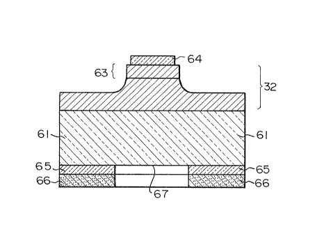
Fig. 27 is a sectional view showing an example in
which the present invention is applied to a mesa type photo-
diode chip. A non-doped InGaAs epi~axial layer 62 is grown
on an Sn-doped InP substrate 61 hy liquid phase epitaxial
process so as to be lattice-matched to the InP substrate 61.
lS Then, a p-type region 63 is formed by Zn diffusion, whereby
a pn junction is produced. Thereafter, a p-side electrode
64 is formed by using AuZn and an n-side electrode 65 is
formed by using AuGeNi.
Further, the chip is etched from both sides in the
neigh~orhood of the pn junction into a mesa shape to reduce
the electrostatic capacity. Then, an Sn plating pattern is
formed on the underside of the n-side electrode 65 using a
plating ~olution of alkanol sulphonic acid. The Sn-plated
portion is herein~fter called a solder layer 66 since it
functions as solder. The solder layer 66 and the n-side
electrode 65 are each in a ring shape, and the underside of
the chip is exposed at the central portion which functions
as a light receiving surface 67. The thickness of the
solder layer 66 is l - 15 ~m. These steps are carried out
by wafer process. Thereafter, the wafer is scribed and
divided into individual chips. The solder layer 66 is
formed efficiently by plating or evaporation. Beside Sn,
Au-Sn eutectic alloy or Au-Si eutectic alloy may be used as
the material of the solder layer 66.
For die-bonding the photodiode chip thus processed
using Sn as the solder, the package to be bonded is heated
to ~50C and the chip with the solder layer 66 attached
thereto is aligned ko the pad and die-bonded thereto. At
~,
- ls~
this time, no other solder is necessary because the solder
layer 66 on the underside of the chip is melted temporarily
and then solidified to fix them securely.
In experiments, the photodiode chip was die-bonded
most satisfactorily when the thickness of Sn plating was
5 - 10 ~m. When the thickness of the Sn plating was 5 ~m or
less, the bonding strength varied and was unstable. When
the thickness of the Sn plating was 10 ~m or more, the Sn
solder overflowed and varled. Therefore, while the optimum
range of the plating thickness depends upon the kind of the
solder material, the plating thickness in the range 5 - 10
~m is generally most satisfactory.
In the present invention, the solder layer is pro-
vided on the chip side. The chip is die-bonded to the
substrate of the package by the solder layer. The substrate
and the package may be arbitrary in the kind of material and
the shape.
Fig. 28 is a sectional view showing the structure in
which said photodiode chip is mounted to a flat type pack-
age using the sapphire substrate 2 of Figs. 8 and 9 producedthrough the steps shown in Figs. 22 to 25. The optical
device chip of FigO 27 is placed directly (without using new
solder) on the die bonding pad 23 and die-bonded thereto to
securely attach the n~side electrode 65 and the pad 23
thereto. The p-side electrode 64 is wire-bonded to the pad
28 by the wire 30. The light passes the sapphire substrate
21 and the opening 24 of the pad 23, and reaches the light
receiving surface 67. In this structure, there is no over-
flow or dislocation of the solder layer 66.
Fig. 29 is a sectional view showing the structure in
which said photodiode chip is mounted to a ceramic sub-
strate type package shown in Fig. 17. Wire bonding, lead
and the external shape of the package are not shown because
they can be selected arbitrarily. In Fig. 29, the ceramic
substrate is not provided with solder, but the solder layer
66 on the chip side functions as the solder to securely
attach the chip to the pad 42.
While the present invention has been described
hereinabove with reference ~o ~he specific applications, it
will be understood that the present invention is applicable
to any of all optical devices such as planar type photo-
diode, avalanche photodiode (APD) and further to packaging
of plane light transmission type light transmitting diode
and plane light transmission type laser diode.
The optical device having the structure according to
the present invention as described above provides the meri-
torious technical effects as follows:
(a) Since overflow or dislocation of the solder layer in
die bonding is prevented, there is no reduction in area or
space of the transparent portion for passing light by the
solder. This increases the yield rate in assembly of the
optical devices. When applied to a photodiode, the present
invention does not decrease the sensitivity o~ the photo-
diode because the photodiode is provided with a metallized
layer of such, for example, as Sn in the die bonding area
other than the light receiving window. Since the thickness
of the metallized layer of such as Sn can be arbitrarily
controlled in the accuracy of 0.2 ~m, there is no overflow
of the solder.
(b) It is not necessary to provide special die-bonding
agent such as solder or epoxy resin in die bonding. This
makes production process simple and productivity high.
While we have shown and described specific embodi-
ments of our invention, it will be understood that these
embodiments are merely for the purpose of illustration and
description and that various other forms may be de~ised
within the scope of our invention, as defined in the
appended claims.
.