Language selection

Search

Patent 1267702 Summary

Third-party information liability

Some of the information on this Web page has been provided by external sources. The Government of Canada is not responsible for the accuracy, reliability or currency of the information supplied by external sources. Users wishing to rely upon this information should consult directly with the source of the information. Content provided by external sources is not subject to official languages, privacy and accessibility requirements.

Claims and Abstract availability

Any discrepancies in the text and image of the Claims and Abstract are due to differing posting times. Text of the Claims and Abstract are posted:

  • At the time the application is open to public inspection;
  • At the time of issue of the patent (grant).
(12) Patent: (11) CA 1267702
(21) Application Number: 530292
(54) English Title: THYRISTOR COMMUTATION CIRCUIT
(54) French Title: CIRCUIT DE COMMUNICATION DE THYRISTOR
Status: Expired
Bibliographic Data
(52) Canadian Patent Classification (CPC):
  • 328/195
(51) International Patent Classification (IPC):
  • H03K 17/72 (2006.01)
  • H03K 17/0814 (2006.01)
  • H03K 17/723 (2006.01)
  • H03K 17/732 (2006.01)
(72) Inventors :
  • HOWELL, EDWARD KEITH (United States of America)
(73) Owners :
  • GENERAL ELECTRIC COMPANY (United States of America)
(71) Applicants :
(74) Agent: ECKERSLEY, RAYMOND A.
(74) Associate agent:
(45) Issued: 1990-04-10
(22) Filed Date: 1987-02-20
Availability of licence: N/A
(25) Language of filing: English

Patent Cooperation Treaty (PCT): No

(30) Application Priority Data:
Application No. Country/Territory Date
839,400 United States of America 1986-03-14

Abstracts

English Abstract


41PS-6368


THYRISTOR COMMUTATION CIRCUIT

ABSTRACT OF THE DISCLOSURE

A commutating circuit in combination with a snubber
circuit are employed to switch a thyristor from a con-
ducting state to a non-conducting state. The snubber
circuit is connected across the cathode and anode of
the thyristor to absorb system energy when the thyristor
is switched. The commutating circuit is coupled in
series with the cathode of the thyristor by means of a
current transformer for increasing the cathode resist-
ance, causing the cathode current to immediately trans-
fer to the gate.


Claims

Note: Claims are shown in the official language in which they were submitted.


- 5 - 41PS-6368

The embodiments of the invention in which an
exclusive property or privilege is claimed are defined
as follows:
1. A thyristor switch circuit comprising:
(a) a thyristor having anode, cathode and
gate electrodes, said anode and cathode electrodes
being connected in a power circuit with a source of
potential;
(b) a commutation circuit for increasing the
impedance of said power circuit and causing thyristor
current to transfer to said gate electrode and
terminating conduction between said cathode and anode
electrodes;
(c) said commutation circuit comprising a
current transformer having a primary and a secondary
winding and a transistor having primary electrodes and
at least one control electrode;
(d) said primary winding being connected in
series circuit with said cathode electrode and said
source;
(e) said secondary winding being connected
in series circuit with the primary electrodes of said
transistor;
(f) means for applying a signal to at least
one control electrode and one of the primary
electrodes of said transistor to switch said
transistor and thus the thyristor between their
conducting and turn off states; and
(g) a snubber circuit connected in parallel
with the series combination of said thyristor and the
primary winding of said transformer for receiving
circuit current from said thyristor when said
thyristor is turned off.
2. The thyristor switching circuit of claim
1 wherein said primary winding comprises one turn and


- 6 - 41PS-6368

said secondary winding comprises a plurality of turns.
3. The thyristor switching circuit of claim
1 wherein said thyristor is selected from the group
consisting of a gate turn-off device and a
silicon-controlled rectifier.
4. The thyristor switching circuit of claim
1 wherein said commutation circuit further comprises a
pair of diodes connected between said base electrode
and the junction of said primary winding and of said
source of potential.
5. The thyristor switching circuit of claim
1 including means connected between the gate electrode
and the emitter electrode of said transistor for
turning on said thyristor.
6. The thyristor switching circuit of claim
1 wherein said snubber circuit comprises a capacitor
connected in series circuit with the parallel
connected combination of a diode and of a resistor.
7. The thyristor switching circuit of claim
2 further comprising a varistor connected in parallel
with the secondary winding of said current transformer
and also with the primary electrodes of said
transistor.
8. A thyristor switch circuit comprising:
(a) a thyristor having anode, cathode and
gate electrodes, said anode and cathode electrodes
being connected in a power circuit with a source of
potential;
(b) a commutation circuit connected in
series with said anode electrode and said source for
increasing the impedance of said power circuit and to
turn off current flow through said thyristor;
(c) a snubber circuit connected in parallel
with series combination of the anode and cathode
electrodes of said thyristor and said commutation


- 7 - 41PS-6368

Claim 8 continued:

circuit for diverting circuit current from said
thyristor when its impedance is increased so as to
turn off said thyristor;
(d) said commutation circuit comprising a
current transformer having a primary winding and a
secondary winding, and a transistor having primary
electrodes and at least one control electrode;
(e) said primary winding being connected in
series with said anode electrode and said source;
(f) said secondary winding being connected
in series circuit with the primary electrodes of said
transistor; and
(g) means for applying a signal to at least
one control electrode and one of the primary
electrodes of said transistor to switch said
transistor and thus the thyristor between their
conducting and turn off states.

Description

Note: Descriptions are shown in the official language in which they were submitted.


1;2~i7~


- 1 - 41PS-6368

THYRISTOR COMMUTATION CIRCUIT

BACKGROUND OF THE INVENTION
When in a conducting state, thyristors remain in
that state until the anode current drops below the hold-
ing current of the thyristor, at which point the thyris-
tor commuta-es to the non~conducting or OFF state. One
prior commutation technique employs the normal reversal
of an AC current. Other known techniques include the
disch~rge of a cornmutating capdcitor into the thyrlstor
to force the current to zero and the increase of the
holding current of the thyristor by forcing a reverse
gate current, as in the gate turn-off (GT0) thyristor.
One method of reversing gate cur~rent in the GTO is call-
ed "emitter switching~' or "cathode switching" and em-
ploys a switching device such as a rnechanical switch or
a transistor switch in series with the cathode of the
GT0 and d pair of diodes to conduct gate current around
the switch when the switch turns off. The switch, in
the 0~ state, must conduct the full GT0 current and, in
the OFF state~ must support a relatively low voltage,
typically in the order of 20 volts. The switch voltage

''7~)~

- ~ - 41PS-6368

drop in tlle ON state must be~very low, on the order of
100 millivolt5~ in order to minimize energy loss. The
purpose of this invention is to describe d thyristor
commutation circuit wit~) extremely low energy loss that
is operated by means of a commutation circuit that is
isolated from the thyristor circuit.

SUMMARY OF THE INVENTION
A commutating circuit is connected in sPries witn a
thyristor that is conducting to rapidly switch the thy-
ristor to a non-conducting state. A snubber circuit is
connected across the thyristor to absorb system energy
to prevent the thyristor from becoming damaged during
the switching operation.
.
BRIEF DESCRIPTION OF THE DRAWINGS
Figure 1 is a schematic representation of a thyris-
tor switching circuit according to the invention for a
GTO; and - --
Figure ? is a schematic representation of a thyris-
tor switching circuit according to the invention for an
SCR.

DESCRIPTION OF THE PREFERRED EMBODIMENT
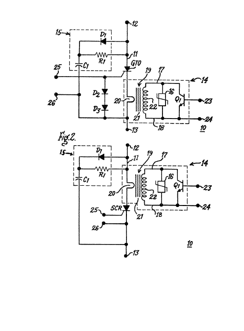
A thyristor circuit 10 is depicted in Figure 1,
wherein a gate turn-off device GTO is connected in
series within a conductor 11 with a voltage imposed
across terminals 12, 13 at opposite ends of the conduct-
or. A commutating circuit 14 is connected in series
with the GTO and a snubber circuit 15 is connected
across the GTO to assist in the commutation and to
protect the GTO from damage once the GTO transfers from
its conducting to its non-conducting state. The commut-
ating circuit is coupled with the GTO by means of a
current transformer 19~ as indicated. The current


.

'7~

3 - 41PS-6368

transfnrnler primary winding 20, which is a single turn,
couples the commutating circuit with the thyristor cir-
cuit by means of the transformer core 21 and secondary
winding 22. A varistor 16 is connected across the se-
condary winding and a transistor Ql is, in turn, con-
nected across conductors 17, 18 and the varistor. In
operation, transistor Q1 is turned on by imposing b~se
drive across terminals 23, 24, which, in turn, effec-
tively shorts the secondary winding 22 so that no ~olt-
age appears across the varistor. To turn on the GTO, apulse is applied over terminals 25, 26 to the gate of
the GTO which is connected to ~he cathode through diodes
D2, D3. When the GTO is conducting and with base drive
applied to the transistor Q1~ no current flows through
the diodes D2, D3. When base drive is removed from
transistor Ql, voltage is generated across the secondary
winding 22 by transformer action of core 21. The volt-
age simultaneously increases across varistor 16, reach-
ing the varistor clamping voltage, at which time the
varistor becomes conductive and a voltage is reflected
across primary winding 20. The voltage across the pri-
. mary winding represents an impedance in series with theGTO, causing the GTO cathode current to transfer to the
gate and diodes D2, D3 rapidly switching the GTO to the
OFF state. The circuit current transfers through diode
D1, and resistor R1, within the snubber circuit 15,
causing capacitor C1 to start charging thereby limiting
the rate-of-change of voltage across the GTO. When it
is desired to switch the GTO back to its conducting
state, base drive is applied to Ql to turn on Ql and a
current pulse is applied across the cathode and gate of
the GTO Yid terminals 25, 26 to turn on the GTO.
An SCR is depicted within the thyristor circuit 10
of Figure 2, connected in series within conductor 11
with a voltage applied across terminals 12, 13. The

- 4 - 41PS-6368

commutating circuit 14 is connected in series with the
anode of the SC~ and the snubber circuit 15 is
connected across the S~R in a manner similar to the
circuit of Figure 1. Base drive is applied to Q1 by
means of terminals 23, ~4 to prevent the voltage from
building up across the secondary winding 22 of current
transformer 19 as well as across the varistor 16. The
commutating circuit 14 can also be connected in series
with the cathode of the SC~ such as with the GTO shown
in the circuit of Figure 1, if so desired. The SCR is
turned on by a current pulse to terminals 25, 26
across the gate and cathode of the SCR. To turn off
the SCR, the base drive to Q1 is discontinued causing
the occurrence of an impedance in series with the SCR,
driving the circuit current through the snubber
circuit 15 via diode Dl, and resistor Rl, to capacitor
Cl, as described earlier.
It has therefore been shown that turn-off of
thyristor devices can be achieved by means of a
commutating circuit and a snubber circuit. The
presence or absence of base drive to the transistor
- connected within the commutation circuit effectively
controls the switching state of the thyristors.


. ", .

Representative Drawing
A single figure which represents the drawing illustrating the invention.
Administrative Status

For a clearer understanding of the status of the application/patent presented on this page, the site Disclaimer , as well as the definitions for Patent , Administrative Status , Maintenance Fee  and Payment History  should be consulted.

Administrative Status

Title Date
Forecasted Issue Date 1990-04-10
(22) Filed 1987-02-20
(45) Issued 1990-04-10
Expired 2007-04-10

Abandonment History

There is no abandonment history.

Payment History

Fee Type Anniversary Year Due Date Amount Paid Paid Date
Application Fee $0.00 1987-02-20
Registration of a document - section 124 $0.00 1987-05-04
Maintenance Fee - Patent - Old Act 2 1992-04-10 $100.00 1992-03-05
Maintenance Fee - Patent - Old Act 3 1993-04-12 $100.00 1993-03-04
Maintenance Fee - Patent - Old Act 4 1994-04-11 $100.00 1994-03-15
Maintenance Fee - Patent - Old Act 5 1995-04-10 $150.00 1995-03-10
Maintenance Fee - Patent - Old Act 6 1996-04-10 $150.00 1996-03-19
Maintenance Fee - Patent - Old Act 7 1997-04-10 $150.00 1997-03-19
Maintenance Fee - Patent - Old Act 8 1998-04-14 $150.00 1998-03-18
Maintenance Fee - Patent - Old Act 9 1999-04-12 $150.00 1999-03-31
Maintenance Fee - Patent - Old Act 10 2000-04-10 $200.00 2000-03-20
Maintenance Fee - Patent - Old Act 11 2001-04-10 $200.00 2001-03-21
Maintenance Fee - Patent - Old Act 12 2002-04-10 $200.00 2002-03-20
Maintenance Fee - Patent - Old Act 13 2003-04-10 $200.00 2003-03-20
Maintenance Fee - Patent - Old Act 14 2004-04-13 $250.00 2004-03-22
Maintenance Fee - Patent - Old Act 15 2005-04-11 $450.00 2005-03-21
Maintenance Fee - Patent - Old Act 16 2006-04-10 $450.00 2006-03-17
Owners on Record

Note: Records showing the ownership history in alphabetical order.

Current Owners on Record
GENERAL ELECTRIC COMPANY
Past Owners on Record
HOWELL, EDWARD KEITH
Past Owners that do not appear in the "Owners on Record" listing will appear in other documentation within the application.
Documents

To view selected files, please enter reCAPTCHA code :


To view images, click a link in the Document Description column. To download the documents, select one or more checkboxes in the first column and then click the "Download Selected in PDF format (Zip Archive)" or the "Download Selected as Single PDF" button.

List of published and non-published patent-specific documents on the CPD .

If you have any difficulty accessing content, you can call the Client Service Centre at 1-866-997-1936 or send them an e-mail at CIPO Client Service Centre.


Document
Description 
Date
(yyyy-mm-dd) 
Number of pages   Size of Image (KB) 
Representative Drawing 2001-05-15 1 17
Description 1993-10-07 4 122
Drawings 1993-10-07 1 20
Claims 1993-10-07 3 102
Abstract 1993-10-07 1 13
Cover Page 1993-10-07 1 13
Fees 1997-03-19 1 69
Fees 1996-03-19 1 51
Fees 1995-03-10 1 56
Fees 1994-03-15 1 71
Fees 1993-03-04 1 45
Fees 1992-03-05 1 61