Note: Descriptions are shown in the official language in which they were submitted.
~ -- 1
Description
_
An Electricallv Alterable ~on-Volatile Memory Device
Bac~ground Of The Invention
The present invention relates to an electrically
alterable non-volatile memory and, more particularly,
to a three-terminal electrically programmable memor~y
cell and a circuit using said cell, having high-
reliability.
Technical Description
Electrically alterable non-volatile memory devices
are well-known in the prior art. A typical device is
an Electrically Programmable Read-Only Memory (EPROM).
An EPRO.~ transistor is a three-terminal transistor in
which the terminals are called the gate, the drain, and
the source. An EPROM transistor is made out of MOS
technology. Within an EPROM transistor is a floating
gate on which charges are stored. The floating gate is
deposited on an insulative layer which separates the
gate from the semiconductive substrate. If the float-
ing gate is neutral, i.e., no charge is stored on thefloating gate, current will conduct from the drain to
the source or vice versa depending on the polarity of
the carrier in the channel between the drain and the
source. If charges are stored on the floating gate,
then the charged floating gate would inhibit current
flow between the drain and the source. The removal of
charges from the floating gate in an EPROM transistor
is done by applying UV or ultra-violet light to the
array of EPROM transistors (typically, a plurality of
EPROM transistors are fabricated from a single semi-
conductive substrate forming an array of EPROM
transistors). The placement of electrical charges on
the floating gates of selective EPROM transistors is
accomplished by applying a high voltage to the gate
35 terminal and a high voltaqe to the drain, causing ..
~æ
-- 2 --
~ 2~ 6
electrons to migrate from the source to the floating
gate. Electrons are injected onto the floating gate by
the mechanism of hot electron injection. Thus, once an
EPROM device (an array of EPROM transistors) has been
subjected to ultra-violet light application, all
charges are removed from all of the floating gates of
EPROM transistors. The application of high voltage to
specific EPROM transistors would cause selective
floating gates to be charged and, thus, selective EPROM
transistors would store representations of data.
Another typical prior art electrically alterable
non-volatile memory cell is the Electrically Erasable
Programmable Read-Only Memory (EEPROM). An EEPROM
transistor is very similar to an EPROM transistor in
that it is a three-terminal device, having a gate, a
drain and a source. The EEPROM transistor also has a
floating gate. However, the floating gate in an EEPROM
transistor has a portion of it insulated from the
semi-conductive substrate by a layer of dielectric less
than approximately 200 angstroms in thickness and is
generally disposed over the drain region. Electrons
are placed and removed from the floating gate from the
drain region through the thin dielectric by the
mechanism of Fowler-Nordheim tunneling. To program an
array of EEPROM transistors, all of the floating gates
of each of the EEPROM transistor are first charged.
That is, all of the EEPROM transistors are activated to
cause the electrons from the drain region to move to
the floating gate. This is accomplished by placin~ a
high potential at the gate terminal, a ground or zero
potential at the source and at the drain. Thereafter,
selective EEPROM transistors are discharged, i.e.,
electrons from the floating gate of selective
transistors are removed. This is accomplished by
applying high voltage to the drain region of the
selective EEPROM transistors and ground potential to
the gate terminal of the selective EEPROM transistors.
MOS transistors are also well-known in the art.
MOS transistors can be enhancement-type, as well as
depletion-type. In an enhancement-type MOS transistor,
a potential must be applied to the gate of the
transistor to cause conduction of current from the
drain to the source. MOS transistors can be made into
either P channel type or N channel type.
In U.S. Patent No. 4,203,158, an EEPROM transistor
is disclosed. In this reference, there is disclosed a
third region in the semi-conductuve substrate, other
than the source and the drain, over which is disposed
the floating gate. The MOS transistor disclosed in
this reference is generally of the EEPROM-type, i.e.,
there being three terminals and conduction of current
between the source and the drain occurs when electrons
are removed from the floating gate. Other references
which disclose an electrically programmable and
erasable memory cell can be found in ~.S. Patent No.
4,132,904; 4,477,825; and 4,274,012. In addition,
reference is made to an article entitled "A New Flash
EEPROM Cell Using Triple Polysilicon Technology" by
Fujio ,Masuka, et al., dated December 1984, published in
1984 IEDM Proceedings, pages 464-467.
Summary Of The Invention
In the present invention, a three-terminal
electrically alterable non-volatile memory circuit is
disclosed. The circuit comprises an MOS transistor
having a drain, a source, and a gate. A first terminal
is connected to the drain. A second terminal is
connected to the source. A programming means for
tunnelling charges has two terminals. One of the two
terminals of the programming means is electrically
connected to the gate of the MOS transistor. A third
terminal is connected to the other terminal of the
programming means.
3~2~ f~6
6681~-416
More specifically, according to a first aspect, the
present invention provides a high rellability non-volatile memory
circult for storing charges thereln comprislng: a pair of MOS
transistors, connected in parallel, each MOS transistor havlng a
source, a drain, and a gate and being of the enhancement type in
the absence of any charge on the gate; a pair of tunnel devices,
each having two termlnals and means for storing said charges; one
of the terminals of each tunnel device being connected to one of
the gates of each MOS transistor; the othex terminals of said pair
of terminal devices being connected together; a pair of
capacitance means, each of sa~d pair of capasitance means being
capacitively coupled to the gate of each MOS transistor; the other
terminals of said pair of capacitance means being connected
together; and programming means, coupled to said capacitance means
and to the other terminal of each tunnel device, for placing said
charges in parallel in said tunnel devices, and on the gates of
said MOS transistors.
According to a second aspect, the present invention
provides a high reliabllity, low power, electrically alterable
non-volatile memory circuit for storing charges therein
comprising: two pairs of MOS trancistors connected in parallel,
each MOS transi~tor having a source, a drain and a gate and being
of the enhancement type in the absence of any charge on the gate;
two palrs of tunnel devices, each device having two terminals and
means for storing said charges; one of the terminals of each
tunnel device being connected to one of the ~ates of each MOS
3a
1267~Z6
66810-416
transistor; two pairs of capacltance means, each being
capacitively coupled to the gate of each transistor; one pair of
said capacitance means electrically connected to the other
terminals of one pair of tunnel devices and the other pair of said
capacitance means electrically connected to the other terminals of
the other pair of tunnel terminals; and programming means, coupled
to said one pair of said capacitance means and to the other palr
of said capaci~ance means, for placing ~aid charges in parallel in
said tunnel devices, and on the gates of said MOS transistors.
3b
-- 4
~Z~ 26
8rief Description Of The Drawings
.. ..
Fig. 1 is a schematic circuit diagram of an
electrically alterable non-volatile memory cell of the
present invention.
Fig. 2 is a cross-sectional view o~ the embodiment
of the electrically alterable non-volatile memory cell
of the present invention, shown in Fig. 1.
Figs. 3a and 3b are schematic diagrams of another
embodiment of the electrically alterable non-volatile
memory cell of the present invention.
Figs. 4a, 4b, 4c and 4d are topological and
cross-sectional views of various embodiments of the
electrically alterable non-volatile memory cell, as
schematically depicted in Figs. 3a and 3b.
Fig. 5 is a schematic circuit diagram of one use
of an EEPROM transistor of the prior art.
Fig. 6 is a high-reliability memory circuit
employing two electrically alterable non-volatile
memory cell of the present invention.
Fig. 7 is a schematic circuit diagram of a high-
reliability, low-power memory circuit employing four
electrically alterable non-volatile cells of the
present invention.
Detailed Description Of The Drawings
Referring to Fig. 1, there is shown a schematic
circuit diagram of an Electrically Alterable Non-
Volatile Memory (EANOM) cell 10 of the present
invention. The EANOM cell 10 is a three-terminal
device comprising a MOS transistor 12 and a tunnel
device 14. The MOS transistor 12 comprises a drain
(D), a gate (G) and a source (S). The MOS transistor
12 is of conventional design. The tunnel device 14 is
a two-terminal device comprising a tunnel oxide and a
terminal, which is connected to the gate (G) of the MOS
transistor 12, and another terminal (T). Thus, the
three terminals of the EANOM cell 10 of the present
invention comprises a first terminal D connected to the
~2~i~7~6
drain of the MOS transistor 12, a second terminal S
connected to the source of the MOS transistor 12, a
third terminal T connected to the tunnel device 14,
with the gate G of the MOS transister 12 connected to
5 the other terminal of the tunnel device 14.
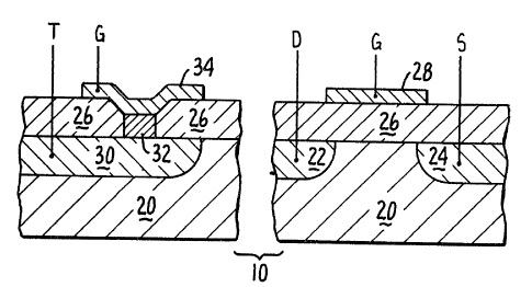
Referring Fiq. 2, there is shown a cross-sectional
view of the EANOM cell 10 of the present invention.
The EANOM cell 10 comprises the MOS transistor 12 a~nd
the tunnel device 14. The MOS transistor 12 is made
10 from a semi-conductive substrate 20 of a first
conductivity type, such as P type. Thus, an N channel
is formed. A first region 22 of a second conductivity
type, such as N is formed in the substrate 20~ A
second region 24, spaced apart from the first region
15 22, is of the second conductivity type, i.e., N . A
first terminal is connected to the first region 22 and
forms the D terminal to the EANOM cell 10. A second
terminal is connected to the second region 24 and forms
the source (S). As is well-known in MOS transistor
20 technology, the surface of the semi-conductive
substrate 20 between the first region 22 and the second
region 24 is the channel of the ~OS transistor 12. A
first insulative layer 26, such as silicon dioxide, is
grown over the semi-conductive substrate 20. A first
25 electrically conductive layer 28 such as a polysilicon
layer is deposited on the first insulative layer 26 and
forms the gate terminal G.
The tunnel device 14 can be fabricated from the
same semi-conductive substrate 20 as the semi-
30 conductive substrate 20 used to fabric~te the MOStransistor 12. A third region 30 o the second
conductivity type is formed in the semi-conductive
substrate 20. The terminal T is connected thereto. A
second insulative layer 32, which can be the same type
35 as the first insulative layer 26, such as silicon
dioxide, is grown on a selected region of layer 30. A
polysilicon layer 34 is deposited on the second
~2~
insulative layer 32. The second polysilicon layer 34
can be the continuation of the first polysilicon 28,
thereby forming the electrical connection between the
terminal G of device 14 and the gate G of the MOS
transistor 12.
In the preferred embodiment, the MOS transistor 12
is an MOS transistor of the enhancement type and, more
particularly, of the N-channel type. The advantage~ of
having an enhancement-type MOS transistor 12 will be
discussed later. The advantage of an N-channel type
MOS transistor 12 is that, in general, an N-channel
type transistor has the advantage of higher frequency
response and greater switching speed. This is due to
the higher mobility of electrons which conduct from the
source through the channel to the drain, rather than
P-type transistors which use holes to conduct from
drain to the source.
The third region 30 of the tunnel device 14 can be
N+ doping of arsenic, buried deep in the region 30.
The second insulative layer 32 in the region
immediately over the third region 30 is preferably less
than 200 angstroms. Thus, electrons can conduct from
the third region 30 to the second polysilicon layer 34
by tunneling through the second insulative layer 32
based upon the Fowler-Nordheim Principle.
The programming of the EANOM cell 10 of the
present invention is accomplished by putting a voltage
potential between terminal T and terminal G, The
application of a high potential voltage (on the order
of 7-15 volts) causes charges to be added or removed
from the second polysilicon layer 34 through the thin
oxide layer of the second insulative layer 32 over the
third region 30. This is due to the tunneling of the
electrons by the Fowler-Nordheim mechanism. Thus, the
tunnel device 14 is the programming means by which
charges (both positive and negative) are added to or
taken off from the gate G. The potential to terminal G
~Zti~ ~26
must be applied through capacitive coupling. This is
accomplished by connecting terminal T to ground;
terminal S is held floating; and terminal D is
connected to a high potential (on the order of at least
10-20 volts). The capacitance of gate G to drain D is
made large enough to provide the necessary capacitive
coupling.
After programming, the terminal G is held at a~
floating state; i.e., not connected to any potential.
Thus, the charges on the gate G remain on the first
conductive layer 28 and affect the conductivity o~ MOS
transistor 12. During the read state, the amount of
current flowing from the source S to drain D determine
the logical state of the EANOM cell 10.
Referring to Figs. 3a and 3b, there is shown
another schematic embodiment, which is the preferred
embodiment, of the EANOM cell 110 of the present
invention. The EANOM cell 110 is a four-terminal cell
and comprises the EANOM cell 10 as shown and as
described in Fig. 1. In addition, a capacitor ~0
having two terminals, 42 and 44, are connected to the
terminal G of the EANOM cell 10 of the present
invention and the drain to gate capacitance is made
small, as capacitor 40 provides coupling. The second
terminal 44 is connected to the terminal G of the EANOM
cell 10 with the first terminal 42 being the terminal C
of the EANOM cell 110. Schematically, the electrical
connection is shown in Fig. 3b. Although
schematically, the EANOM cell 110, 5hown in ~i<~. 3b,
has some 5imilarity to an EPROM transistor, i.e., there
being a drain D, a source S, a control gate C and a
"floating gate" G, there is no terminal T in an EPROM
transistor. Further, it should be emphasized that this
is only a schematic representation and that the EANOM
cell 110 is not comprised in part of an EPROM
transistor.
~2~ 2i~j
Referring to Fig. 4a, there is shown a topological
view of the EANOM cell 110 of the present invention.
Various cross-sectional views of the EANOM cell 110 are
shown in Fig. 4a-1 through 4a-3. F denotes field
oxide.
The EANO~ cell 110 comprises a semi-conductive
substrate 20 of a first conductivity type, such as P
conductivity type. A first region 22, a second reqion
24, and a third region 30, all spaced apart from one
another, are formed in the semi-conductive substrate
20. Each of the regions 22, 24 and 30 are of a second
conductivity type. The terminals D, S and T are
connected to the first region 22, second region 24 and
third region 30, respectively. A first insulative
layer 26 is grown on the semi-conductive substrate 20
and is generally disposed over the first, second and
third regions 22, 24 and 30. The first irsulative
layer 26 can be a material such as silicon dioxide.
Similar to that described for the EANOM cell 10, the
thickness of the second insulative layer 32 over a
portion of the third region 30 is generally on the
order of less than 200 angstroms. A first electrically
conductive layer 28 forming the gate G is deposited
over the first insulative layer 26 and is also
generally disposed over the first, second and third
regions, 22 24, and 30, respectively. The first
electrically conductive layer 28 can be made of heavily
doped polycrystalline silicon. A third insulative
layer 50, such as silicon dioxide, i9 grown or
deposited over the first electrically conductive gate
28. A second electrically conductive gate 52 is
deposited over the third insulative layer 50 and is
generally disposed over the first, second and third
regions 22, 24 and 30, respectively. The second
electrically conductive gate 52 can also be made from
heavily doped polycrystalline silicon. The terminal C
~2~7~
is connnected to the second electrically conductive
gate 52.
The operation of the EANOM cell 110, shown in Fig.
4a, is similar to the EANOM cell 10, shown in Fig. 2.
The only difference between the EANOM cell 110 of Fig.
4a and the EANOM cell 10 of Fig. 2 is the addition of
the capacitor 40. The capacitor 40 is formed by the
second electrically conductive gate 52 and the firs~t
electrically conductive gate 28. Terminal C connected
to the second electrically conductive layer 52 couples
capacitively to the first electrically conductive gate
28 which is one of the two terminals of the tunnel
device 14. The other terminal being terminal T
connected to the third region 30. In all other
aspects, the MOS transistor 12 is the same as described
in Fig. 2.
Referring to Fig. 4b, there is shown in
topological view another embodiment of the EANOM cell
110 of the present invention. Other cross-sectional
views of this embodiment are shown in Figs. 4b-1, 2 and
3. F denotes field oxide region.
In this em~odiment, the second electrically
conductive gate 52 is deposited on the third insulative
layer 50; however, the second electrically conductive
gate 52 is generally disposed only over the first and
second regions 22 and 24, respectively. However, the
application of a voltage to the second electrically
conductive gate 52 (terminal C) causes the second
electrically conductive gate 52 to be capacitively
coupled to the gate G. Since the gate G of the MOS
transistor 12 is connected through the first
electrically conductive gate 2a to the one terminal oE
the tunnel device 14, terminal C is capacitively
coupled to the tunnel device 14 - just like in Fig. 4a.
Referring to Fig. 4c, there is shown in
topological view another embodiment of the EANOM cell
110 of the present i~vention. Other cross-sectional
-- 10 --
'72~
views of this embodiment are shown in Figs, 4c-1, 2 and
3. F denotes field oxide region.
In this embodiment, the second electrically
conductive gate S2 is generally disposed over the
reqion 30. Similar to the embodiment shown in Figs. 4a
and 4b, application of voltage to terminal C causes
voltage to be capacitively coupled to the first
electrically conductive gate 28.
Referrinq to Fig. 4d, there is shown in
1~ topolo~ic~l view a~o~her embodiment of the EANOM ce~l
110 of the present invention. Other cross-sectional
views of this embodiment are shown in Figs. 4d-1, 2 and
3. F denotes field oxide region. In this embodiment,
the second electrically conductive qate 52 is disposed
1S in two parts. One part is over first and second
regions 22 and 24, and the other over the third region
30. This necessitates the application of two control
~ate termina~s, C1 and C2, A schematic representation
of ~his EANOM cell is shown in ~ig, 4d-4,
Capacitors 401 and 402 formed ~etween the first
conductive layer 28 and the two parts of the second
conductive layer 52 are connected to terminals C1 and
C2, respectively. The other capacitor terminals are
connected in common to terminal G,
Having two capacitors for coupling to the floating
gate G allows for selecting a potential to bias
floating ~ate G which is neither the potential at C
nor C2, but some voltage which is the result of the
capacitor divider between capacitor 401 and capacitor
402. This is particularly u~eful in a technique for
read margining a cell following programming, For
example, if read operation was designed to occur with
Ct at ground potential and C2 at ~ , then to test the
margin of conductivity of transistor 12, one could
temporarily tie C2 also at 9round potential, This
would capacitively couple the floating gate G to lower
than normal read potential. If the transistor 12 yet
'7 ~
conducted adequately, a safety margin has been
established which is an indicator of ample positive
charge storage on G.
The programming of the EANOM cell 110 is similar
S to that for the EANOM cell 1 a. A voltage potential is
applied between terminals T and C causing electrons to
move through the second insulative layer 32 to or from
the third region 30. However, because terminal C is
capacitive~y coupled through capacitor 40 - and not
directly connected - t~ the first conductive ~ate 2a ~
terminals C and T can be.c~nnected to a potential, such
as ground, after programming without the loss of charge
on G.
Referring to Fig. 5, there is shown a memory cell
1S circuit of the prior art using an EEPROM transistor 60.
The EEPROM transistor 60 has a gate CG, a floating qate
FG, a source S connected to ground potential, and a
drain D. Ketwee~ the drain D and f~oating ga~e FG,
there is a tunnel oxide area. A select transistor 62
~aving a yate G, a drain D and a source S is connected
to the EEPROM transistor 60 with the source S of the
select transistor 62 connected to the drain D of the
EEPROM transistor 60. ~he select transistor 62 and the
EEP~oM trans~stor 60 are activiated by a voltage
applied to the gate of select transistor 62 and the
gate CG of 60. Current can pass through a resistive
load R which is connected to the drain of the select
transistor 62. At the connection thereof is also the
voltage detection for the output of the memory circuit,
If electrons are on the 1Oating ~ate FG o~ the EEPROM
transistor 60, current would not conduct through the
drain D and source S of the EEPROM transistor 6~ and
thus VO~ would be hi~h. ~f electrons are removed from
the floating gate FG of the EEPROM transistor 60,
current would flow from the drain D to the source S of
the EEPROM transistor 60. This would cause a voltage
drop acrOss the resistive load R bringing VOUt to a low
- 12 -
3LZ~r~ 7Z~
voltage. Both EEPROM transistor 60 and select
transistor 62 are of N channel enhancement type.
The problems of an EEPROM transistor 60 are that
electron gain and loss onto the floating gate can occur
during the reading o the memory cell shown in Fig. 5.
This is because even under read conditions, a minimal
voltage, such as 2.5 volts, must be applied to the gate
G of the EEPROM transistor 60 while the drain coul~
range from 5 volts to zero ~olts, thereby causinq some
charge to be gained or lost from the floating qate,
through the tunnel oxide. In addition, EEPROM
transistor 60 typically fails by the rupturing of the
oxide layer between the floating gate and the drain
after a certain number of charge injection and removal
cycles. Finally, beca~se of electron trapping in the
thin tunnel oxide region between the floating gate and
the drain, there is a possibility of low endurance.
Of all the problems associated with an EEPRO.~
transistor 60, the most severe one is that of rupturing
of the oxide layer between the floating gate and the
drain. This causes the floating gate to be connected
to the drain of the semiconductive substrate, thereby
preventing the storage o~ any charges on the floating
gate. If the EEPX0~ transistor 60 is unable to store
a~y charges, the condition would be as i~ the floating
gate had the drain potential on it. Thus, current can
flow from the drain to the source. In short, a
catastrophic ~ailure would cause the EEPROM transistor
60 to conduct.
Referring to Fig. 6, there is shown a memory
circuit 120, using two EANOM cells 110 of the present
invention which overcomes the problems mentioned
heretofore The two EA~OM cells 11~ have the termina~s
C connected together and are connected to a source of
progLamming voltage labelled "PGM 1". The terminals T
of the EANOM cells 110 are connected together and are
also connected to a so~rce of programming voltage
- 13 -
1~i7i~2~; .
labelled "PMG 2". The ter~inal S of each of the EANOM
cells t10 are connected to ground potential. The
terminal D of each of the EANOM cells 110 are connected
together. A voltage source can be applied through a
resistance R to the drain of the EANOM cells 110. The
output of the memory circuit 120 is at the connection
of the drain of the EANOM cells 110 and the resistance
R.
In the operation of the memory circuit 120,
1V programming is accomplished by placing hiyh-volta~e
potential ~etween PGM 1 and PGM 2. If the ~OS
transistor 12 of each of the EANOM cells 1t0 is o~ an
N-channel enhancement type and if it is desired to
store a negative potential on the gate G of each of the
EANOM cells 110, a positive voltage potential is
applied to PGM 1 with PGM 2 being grounded. This
causes electrons to tunnel from terminal T through the
second insulative layer 32 to the gate G. Once
progr~nming has finished, PGM 1 and PGM 2 are both held
at ground potential. To store a positive potential,
the potentials of PGM 1 and PGM 2 are reversed.
In the read condition, if negative charye is
placed on the floating gate G of each of the EANOM
cells 11~, the MOS transistor 12 of each oE the EANOM
cells 11a, being of the enhancement type, will not
conduct any current from the drain to the source.
Thus, VOUt would be high. On the other hand, if a
positive potential is stored on the gate G of each of
the EANOM cells 110, the positive volta~e on gate 28
would cause each of the MOS transistors 12 to conduct
current from the drain to the source. Current would
then flow through resistance ~ and through each oE the
MOS transistors 12 to ground. VOUt would then be low.
It should be recognized that there are many
advantages to the memory circuit 120, shown in Fig. 6.
First, during the read condition, no external bias is
affecting the charge on the gate G. This is because
- 14 -
7X6
PG~ 1 and PGM 2 are at the same voltage potential,
namely, grounded~ Thus, there is no char~e gain or
charge loss during the read operation. Secondly, by
having two EANOM cell.s 110 of the present invention
connected in parallel, high reliabi~ity ~hrou~h
redundancy i5 achieved. In the unlikely event that the
oxide layer between the third region 30 and the first
electrically-conductive layer 28 ruptures, this wo~ld
cause the tunnel device 14 to short. That is, G would
be connected to PGM 2 and wou~d no longer be able to
hald any cha~ge. Xn that e~ent, however, since the MOS
transistor 12 is of the enhancement type, a ground
potential on G of the MOS transistor 12 would not cause
that MOS transistor 12 to conduct current. Thus, when
there is a short in the tunnel device 14, the
associated MOS transistor 12 is rendered inoperative in
the open circuit mode. It would be as if there were an
open circuit between the drain and the source of the
failed EANOM cell 110. The other EANOM cell 110,
2a however, would continue to function and operate and,
thus, the memory circuit 120 has high reliability, Of
course, many EANOM cells 110 can be connected in
parallel to further increase the reliability of the
circuit 120.
~eferrinq to Fig. 7, theee is shown anothe~ high
reliability memory circuit 150 using EANOM cells 110 of
the present invention. The memory circuit 150
comprises tw~ memory circuits 12~a and 120b of the type
shown and described in ~ig. 6. The two memory circuits
120a and 120b are connected such that the two terminals
C of the EANOM cells 110 of memory circuit 120b are
connected to the two terminals T of the EANO~I cells 110
of the memory circuit 120a and are then connected to
PG~ he two terminals T of the rnernory circuit 12nb
are connected together and connected to the two
terminals C of the memory circuit 120a and are then
connected to PGM 2. A latch circuit 160 is connected
- 15 -
77~
to the resistive loads of memory circuit 120b and
memory circuit 120a.
The latch circuit 160 comprises two P channel
transistors 164a and 164b, and two optional resistive
loads 162a and 162b. The two transistors 164a and 164b
are cross-coupled. The source of each of the
transistors 164a and 164b are connected to the
resistance loads 162a and 162b~ respectively, and ~re
supplied by a power supply +V.
In the programming operation of the memory circuit
150, a potential difference is applied between PGM 1
and PGM 2. The application of a high potential would
cause the gates of one pair ~Pair A~ of the EANOM cells
110 to be charged negative and the gates of the other
pair (Pair B) of EANOM cells 110 to be charged
positive. Reversal of voltage applied to PGM 1 and PG,~
2 would cause the charges to be removed from the gates
of the one pair of the EANOM cell 110 and charges to be
placed on the gates of the other pair of EANOM cell
110. Thus, following programming, the gates of one
pair of the EANOM cells 110 is char~ed positive, while
the other pair is charged negative. This represents
one logical state, such as "1". Application of a
reverse potential would cause the gates of the Pair A
EANOM cells to be charged positive and the gates of the
other pair, Pair B, of the EANOM cells to be charged
negative. This represents the other logic state, such
as "0". The latch 160 detects which of the pairs of
EANOM cells 110 has its gates charged. Thus, the l~tch
160 would then determine the lo~3ical 9tate of the
memory circuit 150,
Similar to the memory circuit 120, once
programmin~ has been accomplished, PGIY 1 and PGM 2 are
connected to ground potential. Suppose now the gates
of the EANOM cells 110 of the memory circuit 120b have
been charged positive, current would flow through the
MOS transistors 12 of the memory circuit 120b.
- 16 -
~ZS~ 6
Conversely, when negative charge is stored on the gates
of the EANOM cells 110 of the memory circuit 120a, the
MOS transistor 12 associated with that memory circuit
120a would not conduct any current. Thus, current
would begin to flow through the resistance Rb
associated with the memory circuit 120b. This would
cause the voltage at the gate of the MOS transistor
164a to be lower than the voltage at the gate of the
MOS transistor 164b. This would cause transistor 164a
to turn on which would cause the potential at the gate
of the transistor 164b ta be pulled up even more.
Transistor 164b would allow the voltage at its drain to
fall. This is an astable condition, and the result is
that the latch 160 permits VOUt to go to the potential
of the power voltage and the voltage potential at the
gate of the transistor 164a to fall to ground.
Transistor 164b would be off and transistor 164a would
be on. However, since there is no conductive path to
ground through the EANOM cells 110 of the memory
circuit 120a, little or no power or current is used.
The analysis set forth above would reverse where the
EANOMs 110 of the memory circuit 120a were charged
positive. Similar to the memory circuit 120, the
memory circuit 150, through the use of paired EANOM
cells 110, has high reliability. As discussed
previously, each memory circuit 120 can comprise more
than two EANOM cells 110 connected in parallel,
It should be recognized that there can be many
applications or uses for the E~NOM cell 10 or 110 oE
the present invention. While the ~IOS transistor 12 has
been described as being of the enhancement type, it
should be recognized that there may be uses for the
depletion type transistors. In addition, of course, P
channel or N channel transistors can be used. In
addition, any capacitive coupling means can be used to
connect the terminal C to the gate of the MOS
transistor 12.