Note: Descriptions are shown in the official language in which they were submitted.
1 ~67~
A CO~DUCTIV~ B~I TE5T SYST~MJ A D~COUPLING ~ErWOR~ ~ER~FO~
BAC~GRO~D O~ TBE I~VENTION
1. Field of In~ention
This invention relates to conducted electromagnetic
interference (EMI) testing and more particularly in a
preferred embodiment to decoupling apparatus and methods used
to determine EMI sources and receptors within electrical
equipment.
2. Description of the Prior Art
Various technigues have been employed to detect, ~1
measure and then suppress E~I in sensitive electrical
equipment or test items. Interference or susceptibility
detection and measuring should be conducted with the test
item operating as close to service conditions as possible.
Also the test item normally is operated in its intended
manner with anticipated inputs applied and its outputs
normally loaded.
A problem exists with simulating service conditions
and normal manner of operation. To bring a test item out of
its normal operating environment and to place it on a bench
for a test, an actual duplication of operation of the test
item seldom occurs. For example, if in a vehicle equipped
with an engine control system that includes a microcomputer
as a controller, assume it is desired to use a particular
portable mobile two-way radio. Discovering that the radio
works when the engine is cutoff but doesn't work well while
the engine is running, the engine control system is then
removed from the vehicle and placed in a bench test
environment for study. A simulator ~support for the engine
control system) is used to make the control system work as
~ ;79~ 1
if it is in the vehicle. Also assume the system responds as
if it is operating in the vehicle controlling what it is
supposed to be controlling. Assume also, the engine control
system generates the same interference that it was putting
out before it was placed on the bench; but now the
interference reacts with the simulator. By virtue of change
in wiring, the coupling between harnesses, other components
and the impedance and length of wires, the engine control
system generally radiates and conducts a different amount of
interference.
',
Efforts have bee~ made to standardize bench test
setups in order to gain data that approaches actual
circumstances.
In prior bench test, under similar circumstances,
line impedance stabilization networks (LISN's) have been
recommended in a number of interference and susceptibility
specifications, for insertion in power leads to offer
something approaching a standard impedance to the radio
frequency (RF) current from test items. The LISN's, as
required by some military specifications introduce a standard
50 ohm power-source impedance for the test item so that
conducted RF interference measurements can be compared to
pass/fail limits without accounting for a source-impedance
variable. But, however, in several ~ISN designs, a 5-
microhenry coil is usedl so the device is suitable for use
from 150 KHz to 25 MHz. Over this range, the source-
impedance varies from about 5 ohms at 150 KHz to 50 ohms at
25 MHz. It is not usable much above 25 MHz due to stray
impedance. While it does furnish a standard impedance, it is
not the impedance seen in the normal installation. It was
never intended to be anything other than an A. C. power line
simu1ator.
~ ~2G793~
Normally when trying to identify the potential of a
device being an interference source, it is thought that this
determination depends upon how you measured the interference
emanating from source. This implies that different test
processes produced different results for the same
interference source. Realizing the a~ove conditions exist,
efforts were made toward devising inteLference measuring
technique that didn't depend upon how the interference was
measured.
BRI~F S~MMARY OF TEE I~VENTIO~
i
¦ The present invention is concerned with apparatus
and methods used for analyzing EMI emissions and/or
susceptible of test items under bench test conditions. A
series of resonators are configured and interconnected in a
particular manner along with a shunt capacitance network to
form a decoupling device. This decoupling device, usually
disposed between the test item and its support system,
provides a means for coupling dc and lower frequency signals
needed for normal test item operations but decoupling
essentially aIl other high frequency signals. Interferring
¦ signals from the test item confront essentially open circuit
impedance with respect to the decoupling network input; and
the test item is forced to produce its highest noise voltage,
the decoupling network acting as a worst case load with
¦ respect to the output of the test item.
Departing from the normal approach to noise studies
of detecting, measuring and then suppressing EMI, using the
decoupling network and testing for worst case interference
parameters provide a repeatable scheme for determin;ng worst
case signals in any environment in which the test item may be
employed~ After establishing worst case inter~erence
parameters, modification technique o~ test item circuit
_ 3 _
L267934
components and connectors may be employed to ~inimize the
affect of generating EMI sources or to immunize susceptible
receptors within the test item.
BRIEF DESCRIPTION OF T~E DRA~ING
Fig. 1 is a side view of a decoupling network
within a block diagram of a bench test setup for analyzing
EMI;
Fig. 2 is block diagram of a noise source with an
unknown impedance being measured using a high impedance
decoupling network to evaluate its worst case noise
potential;
Fig. 3 schematically depicts the decoupling network
of this inven~ion;
Fig. jA is a graphical plot of a number of turns
needed to form resonators at a plurality of resonant
frequencies;
Fig. 4B is a "Q~ curve for a particular resonator;
Fig. 4C is a plan view of the decoupling network;
I
Fig. 4~ is a response curve for a typical bypass
capacitor used in this invention;
Fig. 4E illustrates the response curve for a bank
of capacitors employed as the bypass for this invention;
¦ Fig. 4F is the response curve for the decoupling
network; and
Fig. 5 is a block diagram of a susceptibility bench
test setup in accordance with this invention.
__
Il.
--~- l ~2~7g34
Fig. 6 is a side view ~f a decoupling netw~rk
within a block diagram of a bench test setup for measurin~
short circuit currents.
l DETAILED DESCRIPTION OF A PREP~RRED ~MBODIMæ~T
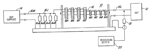
I Fig. 1 is a side view of a decoupling network
I within a block diagram of a bench test setup 10 or analyzing
¦ EMI. A test item or device under test (DUT) 12 is coupled to
its DUT support 14 via a decoupling network 16. The support
,1 14 provides all the power and data signals necessary to
¦~ operate the DUT. Illustratively, the DUT 12 may be an engine
¦¦ control system that includes a microcomputer as a controller
I¦ and the DUT support 14 may be a simulator that makes the
engine control system function just as it would in a vehicle
providing, e.g. the necessary voltages and sensor inputs and
output loads.
¦ Coupled between the input 16L of decoupl;ng network
16 and conventional measurement instrumentation 18, is a
i conventional high impedance probe 20 for coupling noise
signals from the input side of the decoupling device to the
instrumentation. The instrumentation may be the type used to
obtain time or frequency analysis data.
Decoupling network 16 presents a low passband to
the signals from DUT support 14 necessary for DVT operation
and essentially an open circuit impedance to signals from
¦ both the DUT and its support within a chosen frequency band.
Measurements of open circuit noise voltages from the DUT are
desired.
When one is interested in open circ~it voltage
! measurement, you load the DUT into the highest impedance one
j¦ can reasonably obtain. Fig. 2 is a block diagram
1, illustrative o a noise source with an unknown impedance
``- 11 1;~67934
being measured using a high impedance decoupling network to
evaluate i~s worst case noise potential~
To achieve this high impedance, a serially
connected network of resonators has been developed which
opera~e effectively over a broad band of frequencies shunted
by a bank of parallel capacitors which also operate over a
broad band of frequencies. Various compromises are made with
respect to the resonators that are formed and the capacitors
that are used to form the decoupling network 16.
I
In this preferred embodiment, the decoupling
network 16 is designed to produce substantially maximum
uniform input impedance over a frequency range illustratively
from 500 KHz to 300 MHz. ~etwork 16 provides DC resistance
of about 0.8 ohms for DC currents up to about 2 amperes.
To tailor the decoupling network to meet the above
requirements, several steps must be taken along with several
design compromises. Realizing that the intent is not to
design an ideal filter, but rather to design a device that
causes the DUT to emit worst case noise voltages, a high
impedance network should be formed.
Realizing that every inductor resonates at some
specific frequency and that it exhibits its maximum impedance
at its parallel resonance, the limitation on its usefulness
as a decoupling isolator is the "Q~ value which must be high
enough to meet the minimum impedance desired but low enough
to provide an acceptable bandwidth.
To form a high impedance network which spans a
broad range of frequencies, cascaded resonators ~ust be
formed. If maximum "Q" networks are used, a very large
number of high "Q" networks would be required. ~rhus to gain
- 6 -
679~4
a broad band high impedance network yet not employ an
excessive number of high "Q" networks, a compromise should be
made. To form the preferred embodiment one should optimize
the impedance of a chosen number of networks so as to provide
at le~st a minimum impedance of 500 ohms at the maximum
frequency of the voltages that each network will confront.
Also the ~Q" of each coil should be low enough to gain as
much handwidth of coverage for each cascaded impedance.
Typically, parameters for winding inductors are
specified by core manufacturers. The data supplied by the
manufacturers is usually sufficient for winding inductors of
practically any value within the limits of the core and wire
materials. But, however, such data isn't usually suitable
for forming a cascaded set of resonators ~sed in this
invention. Also, with respect to saturation of the core, one
should avoid establishing DC magnetizing forces that would
saturate the core at the desired current range of the
decoupling network. Thus the manufacturers core data should
be consulted for magnetic characteristics of the selected
core material.
Since the decoupling network isn't a filter but a
high input impedance cascaded resonator device, an equivalent
circuit of the decoupling network is depicted in Fig. 3
illustrating the equivalent components. The resonators are
designated 16A-16H. Each resonator is formed from an
inductor in parallel with a resistor and a capacitor to form
a tuned circuit of a chosen center frequency and a specific
"Qn. The parallel capacitance result from stray capacitance
which occur between windings about the toroidal cores. The
resistors result from the DC resistivity of the windings and
the Lagnetic core losses.
~%67913~
A terminating end of the lowest frequency resonator
16H ~nd one end of a gro~nd plane 16K disposed a chosen
parallel distance from the resonators is shunted by a bank of
parallel bypass capacitors, shown in the equivalent circuit
as a single capacitance 16J. The out:put terminals 16M taken
from across the shunt forms a single ended decoupler outp~t.
A lead end of the highest freguency resonator 16A and another
end of the ground plane 16K are connected to an input
~ terminal 16L to form a single-ended decoupler input.
I In establishing the number of resonators needed for
I ¦I the coupling network of Fig. 1, one must take into account
the relationship between ~a) the core material, wire size,
the number of turns of wire employed in constructing cores
that resonate at chosen frequencies and (b) the amount of
bandwidth achieved when lowering the "Q~ to provide for (1)
¦ an optimum impedance across a broadband of noise requencies
without core saturation and (2) a passband for desired
voltage signals. As shown in Fig ~A, there is depicted a
graph of "number of turns" e.g. number 22 wire about a number
of 106 toroidal core versus resonant frequency for the four
lower frequency resonators 16E through 16H. The number 106
core designates a core material of Amidon Associates of North
Hollywood, California. By taking from or adding windings to
the cores, an optimum "Q" and bandwidth for each core at a
¦¦ chosen related resonant frequency is established.
Figure 4B depicts the optimum "Q" for resonator 16H of Fig 4A
calibrated to resonate at 0.8 MHz and providing high
impedance from a lower 3db frequency of 0.7 MHz to an upper
3db fre~uency of 1.0 MHz. Each succeeding resonator is
adjusted similarly to form a family of resonators with
increasing resonant frequencies with overlapping bandwidths
as depicted in Fig 4F.
- 8 -
1.
1~67~
A similar procedure i5 performed for the bypass
capacitors 16J. ~he capacitors are more broad banded th~n
the inductors, thus a fewer number of capacitors are
required. Again we look at the DUT 12 of Fig. 1 and
determine what signal frequencies and voltages are required
for normal operation. For the DUT to operatel the
limitations of the capacitors must be considered. Fig. 4D
depicts reactance versus frequency of a typical capacitor
which might be used with the DUT. It is desired that DUT 12
drive the capacitance; i~e. at operating ranges of
frequencies used by the DUT, so that the capacitor will pass
the signals. As for the interfering signal frequencies, the
capacitors should provide a known, impedance return path to
ground. As in Fig. 4D, normally as you go higher in
freguency, the reactance of the capacitance goes down. When
you continue to go higher in frequency~ series resonance is
reached and the reactance drops way down. At frequencies
above resonancef the reactance rises and then spurious
reactions occurs. The capacitors are not useful in this
region. Thus, as depicted in Fig. 4, the several capacitors
16JA-16JD, that are used as bank of parallel capacitors, are
chosen to provide a low impedance return path to ground for
the noise frequencies but do not significantly alter the
operating frequency signals required by the DUT. Typical
values for the four capacitors are 1., 0.1, .01 and .001
microfarads.
The operation of system 10 will now be discussed.
The input connector 16C of decoupling network 16 is coupled
to D~T 12 and the output connector 16M is connected to the
output of DUT support 14. If we assume that the DUT is the
engine controller mentioned supra, and that it requires dc
and a 12 KHæ clock signal which can be fed from the DUT
sup2ort 14 over the single-ended decoupling network 16 to DUT
~ _g_
Il !
~;~6'79~L
12. If we also assume DUT 12 operates normally when the
signals form DV~ support 14 are supplied due to the pass band
capabilit;es of network 16. The interfering signal voltages
leaving DUT 12 will run into the high impedance of network 16
and be reflected back towards the DU~. Since the input to
network 10 will appear as an open circuit network, the
interfering voltages will increase to establish a worst case
interfering signal voltage. Then a high impedance probe 20
can be connected across the input terminal 16L to obtain a
time or fre~uency domain reading on suitable measurement
equipment 18 of the worst case noise voltage emanating from
DUT 12. Then a variety of suppression techniques may be
employed to minimize this worst case voltage, presenting the
user with an analysis tool that departs from the usual
approach of detecting, measuring and then attempting to
suppress the interfering voltages.
I
Figure 5 depicts another use or the decoupling
network in analyzing the susceptibility of DUT 12 to noise.
Here, a signal generator 22 is used as a substitute
interference source for what are suspected to be potential
interfering devices in the servise environment. The
generator 22 is coupled to the input of decoupling network 16
via a dc blocking capacitor 24 and an attenuator 26. The
attenuator 26 should be connected as close as possible to the
DUT. Suitable measurement equipment 18 may be coupled
through another decoupling network 16 to the input of DUT 12
to gain a measure of susceptibility of DUT 12.
Having developed a broadband high impedance
decouplin~ network to evaluate open circuit interference
voltages, with a minor modification, short circuit current
measurements can be made as well. This will give a measure
of the current potential of interference sources.
- 10 -
1;~67934
Thi~ modified network is shown in Fig.6 where the
6ame capacitor bank 16A-16D is placed at the DUT end ra~her
than at the other end of the network forming a low impedance
load for shunting the interference current to ground. A
current probe 19 is used on this shunted line to measure
worst case interference currents.
~ TABLE_I
¦ Freq. Range: 500 KHz - 300 MHz
Insertion Loss: 80 db or greater
(From Port 16L to Port 16M)
Input Impedance: 500 ohms or greater
¦ TABLE II
Core ~pes: EIGHER FRE~. CORES O.B INCH DIA. IRON PO~DER TOROIDAL CORL
LOWER FRE9. CORES 106 INC~I DIA IhON POWDER ~R~IDAL CORE
Fh 22 Guage Wire 0 Inductance ~MicroHenry)
Ru~2~er ofTurns: 16A 300 MHz 7 4 3~.5
16B 100 12 1. 0 7~. 5
16C 46 22 2. ~ 24+1
161) lB 35 4 . 0 63~3
l 16E 7. 5 Sl 6.5 175~5
: 16F 3. 0 60 9 374~a
16G 1. 5 75 11 582 l 10
16~ .8 100 16 1025~15
Table 1 specifies operating parameters of
decoupling network 16 and Table 2 provides parameters used to
I develop the preferred embodiment of this invention.
A person skilled in the art may make various
changes and substitutions to the layout of parts shown
without departing from the spirit and scope of the invention.
W~AT IS CLAIMED IS.