Note: Descriptions are shown in the official language in which they were submitted.
SWITCHING ARRANGEMENT FOR COMMUNICATION
OF DIGITAL SIGNALS, IN ~ARTICULAR PCM SIGNALS
TECHNICAL FIELD
This invention relates to switching apparatus,
having group couplers and a loop arrangement including a
plurality of single loop lines, for communication of
digital signals, particularly PCM signals, at a fixed
transmission rate to or from connection circuits connected
to a plurality of group buses on each of which parallel
digital signals can be transmitted in a predetermined
number of time compartments in cyclic repetition in pulse
frames.
BACKGROUNp ART
One kind of known switching arrangement or apparatus
is described in commonly assigned U.S. Patent No.
4,500,991, granted February 18, 1985 and entitled "Circuit
Arrangement For the Control of the Transmission of Digital
Signals, Particularly PCM Signals, between Stations of A
Time Division Multiplex Telecommunication Network. . .",
and which corresponds to German Patent No. 2,915,488. In
such an arrangement, it has been found that occasionally
the facilities of connection for the several connection
circuits, which may be subscriber circuits and office
relays, are too sharply limited. Also, the communication
capacity of this switching arrangement has sometimes been
considered inadequate, which has provided a motive for
enlarging the switching arrangement.
To enhance the communication capacity of a switching
arrangement of the kind initially referred to, it might
first occur to one to replace the loop arrangement inter-
connecting the several loop buses by a coupling network.
Coupling networks for time multiplex communications
systems are known in considerahle numbers (NTZ 1970, No.
9, pages 465 to 471). The known coupling networks
comprise space and time stages in various combinations. A
disadvantage of using such coupling networks to...
--1--
~X6796~
er~ance the initially considered switching arrangement, however, is that
the existing circuit structure presupposed by the sw~tching arrangement
would have to be completely altered.
There is 81so known a digital communic&tions system
with divided control (~er Fernmelde-lngenieur, No. 6, June 1984~ in
which use is made of a coupling network consisting of indiYidual coupling
blocks. To expand this ca7munications system, corresponding coupling
stages are provided. A disadvantage here i5 that, depending on load
condition of the communications systern, differing transit times may occur
~ithin the corlrnunications system for a given route.
A main object of the present invention is to further
develop the initially specified switching arrangernent such that connection
facilities for the several connection circuits are expanded, and such that
the corrmunications capacity of the switching arrangement is exp~ndable
in accordsnce with the needs or desires of the situation presented by a
given case.
SUMMARY OF THE INVENTION
The object stated aboYe is accomplished according to
the present invention by an irnproved switching ~rrangement or apparatus
for conmunication of digital signals of n bits esch (for exarnple 8), in
particular pulse code modulated (PCM) signals, at a fixed transmission
rate ~for example 8 kbits/second) to or from connection circuits which
are each connected to~ one of a plurality of group buses on each of which
parallel digital signals of n bits each CQn be transmitted in a total of m x
n tin~e corrpartrnents in cyclic repetition in pulse ~rames, where m is a
preassigned whole nwnber (for example 32) and n is the nwnber of bits
associated with one digital signal. The apparatus has a plurality of
group couplers and a loop arrangement including a plurality of single loop
line~ each provided with first and second connected segments and the
iirst and second segrnents and the group buses are connectable to one
another through the group couplers In the first embodiment of the
.
.. . ..
7~
present invention, the improvement comprises in corr~ination: a plurality
of mQin couplers each being connected to the first and second segments
of the loop arrangement and connectable to first and second line
segrnents of a respective main bus associated with each main coupler, the
first snd second line segments of each main bus serving to trQnsmit digital
si~nals in different directions, and wh~orein each group coupler is
associated with one of the n~in couplers and is connectabIe to the line
segrnents associated therewith.
In this basic embodiment, the invention offers the
advantage that the connection ~acilities ~or the several connection
circuits are considerhbly expanded compared to the known circuit
arrangement initially considered. This is achieved in practice through
the multistage structure of the bus system used, in which the loop
arrangernent is always incorporated.
In a second errbodiment of the improved switching
apparatus of the invention, the loop srrangement further includes a
central timing loop for cQrrying tirning and synçhronizing pulses, which is
provided with first and second connected segments respectively associated
with the first and second segments of the loop srrangernent. The first
segn ent of the central tinnng loop is connectable to a timing pulse
source. The apparatus of this second embodirnent further includes a
plurality of first tDning lines connecting the first and second segments of
the central tD~ung loop to the ITain couplers and a plurality of second
timing lines for providing timing signals between the group couplers and
the connection circuits. An advant~ge which results from this second
errbodiment is that pulse synchronized processing of the several digital
signals is ensured in a comparatively simple manner.
In a third embodiment of the improved switching
apparatus of the present invention, the following features are added to
the.second embodiment. Each main coupler has an additional timing loop
provided with an input connected to the first segment of the central
timing loop. Each additional timing loop is also provided with a pair of
--3--
the first timing lines associated with the first and second line segments of
the associated main bus and is connectable to the second tirning lines
through the associated group coupler. An advantage resulting from this
third errbodirnent is that a cornparatively srnall overall outlay of circuitry
is required to ensure the pulse synchronized processing of the digitaI
signals which are supplied to the several group couplers and/or received
from thern.
In a fourth errbodirr~nt of the improved switching
apparatus of the invention, the following features are added to the
second ernbvdirnent. Each m~in coupler has all addi~ionhl tirning loop
formed from one of the first tirning lines and provided with an input
connected to the first segment of the central tirning loop, a first segment
for supplying tirning pulses, and a second segment for returning tirning
pulses connectable through the associated group coupler to one of the
second tirning lines leading to at least one associated connection circuit
arranged for sending digital signals. Each rnsin coupler also has another
one of the first timing lines connectable through the associated group
coupler to snother one of the second timing lines leading to ~t least one
sssociated connection circuit arranged for receiving digital signals. An
advantage of this fourth embodirnent is that the pu}se synchronized
processing of the digital signals to be supplied to the seversl group
couplers and/or picked up from them becomes practically independent of
line lengths.
A fifth ernbodiment of the present invention has
additional elernents which can be incorporated into any of the
aforementioned embodiments of the invention. In the fifth embodirnent,
each loop line of the loop arrsngement in the improved switching
apparatus is operatively arranged such that digital signals of at least n
bits each can be transrnitted in pulse frarnes occurring in cyclic repetition
in a predeterrnined whole nwnber p (for exarnple 32) of successive time
cornpartments from its first segment to its second segrnent. Also, each
main coupler hss first exchange rneans for transferring in an outgoing
direction to the first segments of the single loop lines of the loop
--4--
~26~9~
arrangement vis the associsted group coupler digitsl signals from at least
one associated connection circuit arranged for sending such digitsl
sign~ls, the first exchange means including parallel-to-serial conversion
means and a space-time stage connected thereto, and second exchange
means for transferring in an incoming direction from the second segments
of the single loop lines of the loop arrsngement via the associated group
coupler digital signals to be transmitted by at least one associated
connection means arranged for receiving such digital signals, the second
exchange means including a space-time stage and serial-to-parallel means
connected thereto.
An advantage which results from the fifth embodiment is
that a cornparatively sn~ll overalI outlay of circuitry is required for
considerable expansion of the cormlunication capacity of the loop
arrengement and hence of the system as a whole, since a corresponding
numoer of loops are provided for the loop arrangement. This advantage
becomes especially clear when a subsequent eXpQnSiOn of the capacity of
the system is contemplated.
The sixth embodiment of the present inv~ntion adds to
the fifth ernbodirnent in the following manner. In each main coupler of
the sw~tching apparatus of the sixth ernbodiment, the first exchange means
further inciudes an inverter and first ~nd second registers arranged in
series between the serial-to-parallel conversion means and the first line
segment of the associated main bus. Ille outputs of the first register are
connected to the serial-to-parallel conversion means and the inputs of
the second register are connected to the first line segment. l}le first
segrnent of the central timing loop is connected by one of the first tin~ing
lines directly to the space-time stage, the serial-to-parallel conversion
means, the first register and the inverter, nnd through the inverter and
the additional timing loop to the second register, in order to provide
timing signaLs thereto. The second exchange means further includes a
third register arranged between the parallel-to-serial-conversion means
and the second line segrnent of the associated main bus, and the second
segment oi the central tirning loop is connected to the space-time stage
--5--
~2~9~;~
and the parallel-to-seriHl conversion rneans in order to provide timing
signals thereto, and the output of the inverter is connected to the third
register in order to provide timing signals thereto. The advantage which
results from the sixth ernbodiment is that there is an especially lo
overall outlay of circuitry required to implement the main couplers.
In a seventh ernbodiment of the switching apparatus of
the present invention, the loop lines of the loop arrangernent and the
central timing loop are each of such length thfit the digitsl signals and
timing pulses respectively transmitted thereover experience a transit tirne
corresponding to a maximwn phase shift of 180 degrees as detern~ined witl~
reference to the digital signals and timing pulses respectively delivered
to them. The advantage of the seventh embodiment is that secure or
reliable operation of the entire switching apparatus is facilitated for any
appreciable, that is reasonable, length of the loop arrangement. As will
become app~rent later, the length of the loop in question may be up to ~0
meters at ordinary PCM signal frequencies.
The eighth embodirnent of the invention adds to the
fifth ernbodiment~ In the eighth errbodiment, in each m&in coupler the
first exchange means further includes first and second registers arranged
in series between the seri~l-to-parallel conversion me&ns and the first
line segment of the associated main bus. A1SOJ the first segment of the
central tirning loop is connected by one of the first timing lines directly
to the space-time stage, the serial-to-paralIel conversion rnesns, the first
register and through the additional timing loop to the second register to
provide timing signals thereto. Moreover, the second segrnent of th
central tirning loop is connected by another one of the first tirning lines
to the space-tirne stage and the serial-to-parallel conversion rnPans of
the second exchange means to provide tirning signals thereto. An
advant~ge of the eighth errbodiment is that there is an especially low
overall outlay of circuitry for an alternative embodiment of the main
coupler.
6~
Integrated storage t~ns switch circuits msy be used il
desired ~n those of the foregoing embodiments of the present invention
which require space-time stages in their rnain couplers. This constitutes
the ninth en~diment of the invention, and has the advantage that an
especially low overall outlay is accordingly required for the space-time
stages in esch mQin coupler.
A tenth errbodirnent of the invention builds upon the
fifth ernbodiment of the present invention by providing the following
additional features. In ths first exchange means o~ eAch r~in coupler,
the space-time stage has x inputs and the parallel-to-seriRl conversion
msans has n inputs ~nd x outputs and is operatively arranged such that
digital signals presented in parallel to the n inputs of the parallel-to-
serial conversion rneans are successively delivered as serial words of n
bits each to the x inputs of the space-tirne stage connected thereto
Also, in the second exchange means of esch main coupler, the space-tims
stage has x outputs and the seri~l-to-parallel conversion means has x
inputs and n outputs and is operatively arranged such th~t serial digital
signals of n bits each presented by the space-tirne stage to the x inputs
of the serial-to-parallel conversion rneans are converted to digital signals
occurring in parallel on the n outputs thereof, and wherein x is a
positive whole nurnber satisfying the condition that x is less than or squal
to n. The tenth errbodiment affords the advantflge of parallel-to-serial
and serial-to-parallel conversion means of especially simple construction.
BRIEF DESCRIPTION OF THE DRAWINGS
.
Fig. 1 shows an embodiment of the switching
arrangernent according to the invention by way of example.
.
Fig. 2 shows a rnodification of main couplers used in the
circuit arrangement according to Fig. 1.
Fig. 3, in a pulse diagram, illustrates tl?e forrn oî pulses
at various switch points in the switching arrangemsnt of Fig. 1.
--7--
7~
Fig. 4, in a pulse diagram, illustrates the forrn of pulses
at various switch points in the switching arrsngernent represented in Fig.
2.
D~TAILED DESCRIPTION OF THE PREFERRED EMBODII~ENTS
With reference to the drawings, the embodiments of the
invention described above w~ll be further illustrated belou~ by way of
example.
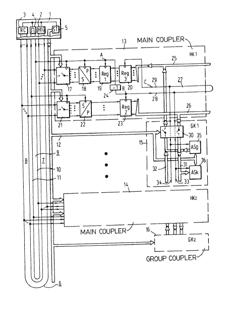
The switching arrangelrent or apparatus represented in
Fig. 1 comprises a central control meflns 1, which -- like the known
switching arrangement initially contemplated -- cornprises audio
generators (HTG) 2, receiving means (RC) 3, a timing pulse source 4
delivering timing and synchronizing signals, and a tirne channel assignment
circuit 5 assigning the time channel or compartment used within cyclically
recurring pulse frames for given routes to the several units. The units 2
to 5 in question may, as indicated in Fig. 1, be interconnected by way of
a line arrangen?ent.
To the central control means 1 is connected a loop
arrangement 6 co~Tprising a plurQlity of individual loops, for example eight
individual loops, each having a first segment 7 and a second segment 8
connected thereto. ll-e operation of the several loops of the loop
flrrangement 6 is such that a definite number P) (for exarnple 32) of time
compar~nents of n ~=8) bits each are each defined upon them in
successive pulse fr~nes cyclically repested. This corresponds to the
customary flow of data on a 2.048 MHz PCM transmission line. The audio
generators 2 n~y assume the same functions with respect to the receiving
means 3 as do the corresponding units in the known switching arrangement
initially contemplated. The number of loops flnd/or of time compar~ents
occurring per pulse frame may be greater than specified above when a
higher traffic capacity is called for.
--8--
i79~i~
Besides the central loop arrangernent 6 considered
above, in Fig. 1 a central tirni~ loop 9 is provided coiTprising a first
segment 10 and a second segrnent 11 connected therewith. Segment 10 oî
this central timing loop picks up the timing pulses delivered by the timing
pulse source 4, and segrnent 1~ delivers the ti~ng pulses in question to ~
sign~l sink or monitor circuit in the timing pulse source 4. The central
timing loop 9 with its loop segments 10 and 11 is associated with the
segments 7 and 8 of the central loop arrangement 6, and in practice, is
preferably topologically associated as well. This ensures that signals
occurring Gn the seg~nents associated with each other in a given case willl
have the sarne velocities of propagation.
Besides the line arrangements discussed above, an
omnibus line 12 is provided in Fig. 1 as well, by WRy of which information
is conveyed from the time channel or comp~rtment assignment system 5 to
the SeverRI units to be controlled through the time comparlments or
channels to ~e utilized in a given cQse. This will be further discussed
later on.
The switching arrRngement represented in Fig. 1 further
co~rprises mQin couplers (HKl to HKz) 13, 14, of which 8 plurality, for
exarnple eight, n~y be provided, snd which are connected to various
locations on the segments of the central loop arrangement 6 and the
central timing loop 9. To each of the main couplers 13, 14, in iFig. 1 at
least one group coupling means (GXl, GKz) 15, 16 is connected, each
containing a group coupler. These group coupling means n~y be groups
of c~nnections such as those that are connected by way of group couplers
to the loop provided in the knou~ switching arrangement initially
considered.
Now the main coupler 13 will be considered more
closely. It comprises two space-time stages 17, 21, each of which msy
preferably be cornposed of integrAted storage time switch arrangements
such as are com~ercially svailable (for example3 from the firm of Siemens
AG under the trade designation PEB 2070. The space-tirne stsge 17 is
_g_
connected on its output side to the segments 7 of the central loop
arrangement 6. The stage 17 in guestion is connected on its input side
to x outputs (where x is less than or equal to n) of R parallel-to-serial
conve~ion means 18, which is connected on its input side to the output
of a first register ~Reg 1) 19. This register 19 is connected on its input
side to the outputs of another register (Reg 3) 20, which is connected on
its input side to segrnent 25 of a msin bus. Besides the segrnent 25 in
question, this main bus includes an additional segment 26 thus enabling
digital signals to be transmitted bidirectionally on the main bus, as ~nay
be required in any given case.
The other space-time stage, stage 21, is connected on
its input side to segments & of the central loop arrangement 6. On its
output side, stage 21 is connected to x inputs (where x is less than or
equal to n) of a series-parallel conversion rneans 22, which is connected
on its output side to the ssid other segrnent 25 of the main bus, comprised
of segments 25 and 26, and associated with the main coupler 13.
1'he space-tine stages 17 and 21 of the m~;n coupler 13
are connected by control inputs to the omnibus line 12. By way of this
line 12, the space-tin~ stages 17, 21 receive setting info~tion
regarding the thne channels or cornpar~nents to be used within pulse
frames occurring in cyclic repetition for their connection to the central
loop arrangement 6, and regarding the spatial relaying o~ signals.
The space-time stage 17, the p~rallel to-serial
conversion means 18 and the register 19 are connected by tin~ing inputs
to segment lU of the central tirning loop 9. By way of an inverter 24,
the timing line in question is connected to the t~Ting input of the
register 23.
The timing inputs of the space-tin~ stage 21 and of the
serial-to-parallel conversion means 22 are connected to segrnent 11 of
the central timing loop 9.
--10--
79~
To the output of the inverting element 24 is likewise
connected on segment 28 of an additional tirning loop line 27 connected
by a segment 29 to the timing input of the register 20. The additional
timing loop 27 is associated with the l7~in bus having the two se~rnents
25, 26, and its two segments 28, 29 may be disposed ~ex~ctly like the two
segments 26, 25 of the main bus in question.
'rO the n~in bus comprising segments 25, 26 ~nd to the
additional timing loop 2?t in Fig. 1, is connected the group co~lpling
means 159 by way of a group coupler 30 having group buses 31, 32 ~nd
t~ng lines 33, 34 on its other connecting side. To group bus 32 and
tin~ng line 34, which latter may be connécted directly to the timing line
segment ~9, in Fig. 1, is connected ~ connection circuit (ASg) 35, which
is to deliver digital signals. To group bus 31 and tLning line 33, of which
the latter may be connected directly to the tirning segment 28, is
connected a connection circuit (ASk) 36 c~p~ble of picking up or
receiving digital signals. The two connection circuits 35, 36 Qnd the
group coupler 30 are connected by setting inputs received from the
~bove-mentioned omnibus line 12. The two connection circuits 35, 36
may pertain to one and the same subscriber circuit or rel~y means.
Overall, a plurality of them are provided.
Before going on to the mode of operation of the
switching ~rrangement represented in Fig. 1, the r,~di~lc~tion represented
in ~ig. 2 for the main coupler shown in detail in Pig. 1 will be discussed.
The mQin coupler (HK) 40 represented in Fig. 2 comprises two space-time
stsges 41, 45, connected, similarly to the space-tine st~ges 17, 21 of Fig.
1, to the central loop arrangement 6. The spsce-time stage 41 is
connected on its input side to the output side of a parallel-to-serial
conversion means 42, which in turn is connected on its inputs side to the
outputs oi a register (Reg 4) 43. This register 43 is connected on its
input side to the outputs OI another register (Reg 5) 44, which is
connected on its input side to segment 25 to the main bus previously
mentioned in connection with Fig. 1, to which segment 26 likewise
perte.ins. To this segrnent 26, in Fig. 2, is connected the output of a
79~
serial-to-parallel conversion me~ns 46, which is connected on its input
side to the outputs of ths space-time stage 45.
ln contrast to the situation repr~sented in Fig. 1, in
the circuit arrangement represented in Fig. 2, to the timing connection
line connection to the timing inputs of the space-time stage 41, the
parallel-series conversion means 42 and the register 43, is connected ehe
signals input of Another timing loop 47, which in turn is connected on its
output side to the tirninK input of the register 44. Timing loop 47 with
its two segments may be disposed just like the two seglr~nts 25, 26 of the
main bus. Further, the timing line connected to the tirning inputs of the
spAce-time st~ge 45 and of the serial-to-parallel conversion means 46 is
continued as a timing line 48. The timing pulses o~curring on the return
segrnent of the additional timing loop 47 and timing pulses occurring on
timing line 48 are delivered to the current group coupling meflns, which is
connected to the main coupler 40.
The mode of operation of the switching s~r~ngernent
re~presented in Figs. 1 and 2 will be described shortly. First, however,
with reference to Fig. 1, it is noted th~t the several group coupling
means, such as group coupling means 15, are so constructed thflt the
segments of their group buses, such ~s segrnerJts 31 and 32, each comprise,
for exsrnple, n - 8 single lines, on which ~ bits belonging to one binary
signal, or PCM word occur in parallel at ~ given time. Here provision is
rn~de so thst within pulse frames cyclically repeated at ~ rate of 125
microseconds, m x n = 256 tirne slots are determined in each instance on
the several segments 31, 32, so that, per group coupling means, 256
different time slots, or compartments, are available in the outgoing
direction of transmission and 256 slots or corrparbnents in the incoming
direction, wherein this case m is 32.
The digit~l signals occurring on the severAl lines of
segrnent 32 of the group bus of Ule group coupling rneans 15 are supplied
to a corresponding number (eight) of inputs of register 20. By this
register 20, the digital signals successively occurring are t~ken over by
--12-
'' ' . :,`.`' : - . .
7~
timing control. Then the digital signals in question srise in register 19,
from which they are successively supplied by way of the parallel-to-serial
conversion mesns 18 to various (for example eight) inputs of the space-
time stage 17. Th;s procedure may be such thst the parallel to-seri~l
conversion me~ns 18 successively delivers from its vsrious outputs serial
digital signals corresponding to the parallel digital signals supplied to it
on its input side. These digital si~na]s, with their bits occurring serially,
or PCM signals, are supplied by way of a space-time st~ge to one of the
loops of segrnent 7 of the central l~op arrangement 60 In stage 17,
accordingly, there occurs a sp~tial and a temporal conversion of the
digitQI signal, such as a PCM signal, supplied to it st a given time. The
digital or PCM signal delivered by the space-time stage then occurs ~s a
signal comprising for example eight bits in one time con~partment out of
for ex~ le 32 compar~nents in ~ pulse frarne pre~ailing on the particular
loop of the centraI loop ~rrangement 6.
The bits of digital signals, or PCM sign~ls, occurring
serially on segrnents 8 of the several loops -- which may ~or example be
eight in number -- of the central loop arrangement 6 are picked up at
the scheduled times by the time stages, corresponding to space-time stage
21, of the main coupler. Ihe digital signBls picked up by space-time
st~ge 21 then arrive at several (for example eightJ irlputs of -the serial
to-parallel conversion means 22 connected therewith, which thereupon
forwards the digital sign~ls, converted into parallel form, by way of for
example eight parallel lines to register 23. Register 23 ~orwards the
digital signals in question to segment 26 of the associated main bus.
In the switching arrangement represented in Fig. 2,
processes entire~y corresponding in principle to those explained above
with reference to Fig. l take place. The only essential difference
between the switchin~ arrangement represented in Fig. 2 and that
represented in Fig. 1 consists merely in that the switching ~rrangement
represented in Fig. 2 dispenses with any register corresponding to the
register 23 snd inverter 24 of Fig. 1.
--13--
~67~6~
A comnon feature of the switching srrangement
represented in Figs. 1 and 2 is that the digital or PCM signals are
transmitted in parallel on segrnents 25, 26 of the main bus in question and
that they occur AS serial digital or PCM signals on segments 7, 8 of the
several loops of the central loop arrangement 6. If in this context we
consider a connection from one connection circuit delivering digit~l or
PC~5 signals, such as connection circuit 35, to a connection circuit
picking up or receiving such si~nals, such as connection circuit 36, then
the switching arrangement illustrated turns out to be an exchange
switching system in which we have first a tirne stage (in the group
coupling me~ns 15 comprising connection circuit 35~, then a space and
tin~e stage (in stage 17), then a space-time stage ~in stage 21), and
finally a time stage again in group coupling means 15 with connection
circuit 36. Over~ll, this requires three different time compartments or
channels: one time c~npartment or channel on segment 32, 25, one time
compartment or channel on one of the loops of the central loop
arrangenent 6, and one time cornpartment Dr channel on segment 26, 31.
In the mode of operation of the switching arrangements
represented in Figs 1 and 2 as just outlined, the situation with respect
to the timing control of the several units has been disregarded for the
sal~e of sLmplicity. The timing situation in question is illustrated in Figs.
3 and 4. Figs. 3 and 4 thus illustrate the behavior of timing signal
voltages IJ at various switch points A, B and C in Fig. 1 and A and B in
Fig. 2 as iunctions of time t.
Fig. 3, in the line marked A, shows the form of the
timing pulses occurring at switch point A in Fig. 1, which may occur at a
seri~l frequency of 2.048 MHz. This meQns th~t the period of these
pulses is about 488 nsec. In line B, Fig. 3 shows the form of the timing
pulses occ~lrring at switch point B in Fig. 1. Line C1 illustrates the
timing pulses occurring at switch point C in Fig. 1 in the csse where the
timing loop 27 is assigned a length such that there is a timing pulse delay
by tl of about 244 nsec. C2 in Fig. 3 designates timing pulses occurring
at switch point C in Fig. 1 in the case where the timing loop 27 is shorter
-14--
36~
than in the case previously considered. The effecls of the delays in
question are indicated in Fig. 3 by arrows between ~he corresponding
pulse sequences.
From Fig. 3 ;t JT~y be seen that between the pulse
sequences represented in lines B and C1J there is a phase shift of 180,
or a time shift T1 of about 244 nsec. Between the puIse sequence
represented in lines B and C2, there is a phase shift corresponding to a
time interval T2 sma}Ier than the tirne interval Tl. Asswning a transit
time of 6 n~noseconds/meter for the tr~nsrnission lines used, this means ~
rnsximum length of about 40 meters for the timing loop 27 in the eas~e
~/Cl. Be it noted here that the central t~ming loop 9 and hence the
central loop arrangement 6 in Fig. 1 will be o corresponding length.
If -- as Fig. 3 suggests -- it is considered that the
anterior flanks of the tirning pulses occurring at the several switch points
A, ~, C serve ~or ti~ning control of the several units, then it r~y be seen
from ~ig. 3 that in R situation corresponding to lines A and Cl, there is a
sirnultaneous pick-up ~et tl) of the digital sign~ls occurring on segment
25 of the main bus by register 20 and register 19, whereas in the
situation corresponding to lines A ~nd C2 in ~ig. 3, there is first a pick-
up of the digital signals oceurring on segrnent 25 by register 20 (at time
t2) ~nd then a pick-up by register 19 (at time t3). In this way, phase
differences between pulses prevailing on the central timing loop 9 and the
"decentral" additional tirning loop a7 are compensated. At the same
time, this cornpensates for phase differences between the digital signals
occurring on the central loop ~rrangement 6 and on the several segments
of the main buses and the group buses shortly connected with them.
- Fig. 4 illustrates the situation, corresponding to that
previously illustrated, respecting the switching arrangement represented
in Fig. 2. Ilere the pulse forms shown in lines A and B1 of Fig. 4
illustrate the case where the timing pulses occur at switch point B in Fig.
2 are shifted in phase from the timing pulses occurring at switch point A
therein by 180~ (T1 nearly equsl to 244 nsec.), QS indicated by a
-15-
~3L267~
corresponding arrow. Line B2 illustrates the timing pulses occurring At
switch point B in Fig. ~ for the case where a shorter transit time (see
arrow) is to be anticipated fsr the timing pulses occurring on ti}ning loop
47 in Fig. 2. This trsnsit tirne is indicated in Fig. 4 by T3.
From Fig. 4, then, the following m~ be seen: If the
tirning pulses occurring on timing loop 47 in Fig. 2 suffer a delay of T1
relatjve to the timing pulses occurring at switch point A, then the digital
signals occurring on segment 25 of the main bus of the main coupler 40
are picked up in register 44 at the time t4 and picked up by the following
register 43 at a time tS. If the delsy between the timing pulses
occurring at switch poin~s B and A in Fig. 2 has a duration of T3, ~en
the digital signals occurring on segment 25 in Fig. 2 are picked up in
register 44 at the tirne t6 and in register 43 at a time t7. In this case
also, a compensation for phase differences prevailing between pulses on
the central timing loop 9 and timing loop 4~ is achieved. In this case
also, trsnsit time problems are solved, as they were solved in the
switching arrangement represented in Fig. 1.
With reference to Figs. 3 and 4, it may be sdded that
in the case of the embodiment o~ FigJ 1~ the loops o~ the central loop
arrangement 6 and the tirning loop 27, given a transit time of 6
nanoseconds/meter, n~y have a maximwn length of about 40 meters, and
that in the err~odiment of Fig. 2 the lengths oî the loops and tinung lines
are imnaterial in practice for purposes of maintaining proper operation at
all times in conjunction ~nth the given main coupler snd the m~in bus
connected ~erewith. With the assumed transit times on the several
lines, the lines of the central loop arrangement and of the central timing
loop will be of corresponding lengths.
.
As initially mentioned, information concerning the time
compartments or channels to be used from t~me to tim~ is transmitted from
the- time channel or compartrnent assignment means 5 to the several units
to be controlled by way of the omnibus line 12 indicated in Figs. 1 and 2.
To be able to convey this information, the time channel or compartment
-16-
~Z~ 36'~
assigning means 5 first requires appropriate data. For this purpose, the
central control unit 1, by way of separate polling channels ~not explicitly
shown), obtains calls from currently calling line connections. In the
context of this inquiry, both the calling stations and the stations to be
called, or the addresses designating these stations, are recorded. ~ese
data sre then stored, together with data on the time compartments or
channels assigned to the call in question, in coordination tables whose
contents will serve to trigger the several units by way of the o~ibus line
12. The polling means thus required and the coordination tables sn~y
therefore be part and parcel of the time channel or comparbnent
assigning system S.
In conclusion, it ~r~y be added that while the present
invention has been illustrated in terms of switching arrangements in which
the digital signals or PCM signals are transmitted serially by way of
individual loops of the central loop arrangement 6, it should be noted
that the subject matter of the present invention may dispense with such
serial transmission of the digital signals or PCM signals if the parallel-to-
serial and serial-to-parallel conversion means are eliminated.