Note: Descriptions are shown in the official language in which they were submitted.
9~i5
~, ~c i
FIELD OF THE INVENTION
The present invention relates generally to
semiconductor structures for analog or digital applications
which have ambipolar or unipolar current modulated by electric
fields produced due to a voltage applied to a control
electrode, and more particularly to two classes of field effect
transistor structures which may respectively be called DIFETs,
for double injection field effect transistors, and VMITs, for
vertical modulated injection transistors. Both DIFETs and
VMITs have an intrinsic or doped semiconductor region or body
located between two or more current path electrodes and at
least one gate or control electrode located adjacent to or
within the intrinsic region for modulating or switching the
ambipolar or unipolar current flo~ing between such current path
electrodes by voltage applied to the control electrode.
BACKGROUND OF THE INVENTION
The explosive growth of semiconductor technology in
the past several decades has produced a variety of transistor
devices~ almost all of which enable the current through two
terminals of such a device to be controlled by a signal
supplied to a third terminal. One such transistor ls the
bipolar transistor, which includes an emitter formed of a first
conductivity type, a base formed of a second conductivity type,
and a collector formed of the first conductivity type. At
least one amorphous silicon (a-Si) bipolar transistor has been
investigated3 as described in the Japanese Journal of Applied
Physics, pp. 714-715 (Sept. 1984).
3~ The technology has produced a number of field effect
transistors (FETs). In the typical field effect transistors,
the current in the active region or conduction channel of the
FET ls formed by carriers of one polarity only, that is, the
number of carriers of the other polarity in the current, if
any, is operationally insignificant~. One such FET is the
junction field effect transistor, or JFET, in which the voltage
supplied to a gate electrode varies the depletion width of a
reverse biased p-n junction formed between the gate electrode
- and the current conducting channel. The conductivity of the
channel is modulated by varying the percent of that channel
., -1-
,
879.1 ~ 9~
which is depleted as a result of voltage applied to the gate.
A similar device called the metal-semiconductor FET, or MESFET,
has a gate electrode made of a metal which forms a Schottky
barrier with the semiconductor material of the conducting
channel. Another well known type of field e~fect transistor is
one in which the gate electrode is separated from the
semiconductor channel by an insulator. Perhaps the most well
known of such insulated gate transistors is the
metal-oxide-semiconductor FET, or MOSFET, in which a metal gate
is separated from a semiconductor channel by a silicon oxide
insulator.
Also relevant to the background of the present
invention are those earlier field effect transistors in which
the semiconductor material connected between the two current
path electrodes is sufficiently conductive to allow current
flow in the absence of either an applied field created by a
control electrode. Such transistors include the JFETs and
MESFETs described above, in which the depletion region formed
by contact of the transistor's semiconductor channel region
with its gate electrode can be expanded or contracted by
applying a control voltage to the gate electrode.
A somewhat similar device is the depletion-mode MOS
transistor. This transistor differs from the JFET and the
MESFET just described in that its gate electrode is
electrically insulated from its semiconductor channel.
However, it is similar to those devices in that its
semiconductor channel is normally Uon", or conducting, in the
absence of a voltage applied to its gatP electrode and requires
the application of a voltage to its gate electrode to shift the
Fermi level of its channel so as to deplete that channel of
majority carriers, and turn the transistor "off" to make it
non-conducting.
The MOSFETs mentioned above also can be operated in an
enchancement mode9 wherein a voltage is applied to the gate to
induce a channel of minority carriers in a doped substrate
between the source and drain, thereby allowing the minority
carriers to flow therein in response to a voltage applied to
the source and drain. Enhancement mode MOSFETs have found wide
application, and, for example, are the building blocks from
which CMOS devices are made.
879.1
Various transistor structures having a gate or grid
electrode inside the transistor be~ween two current-carrying
electrodes have also been disclosed over the past three
decades. In U.SO Patent No. 3,385,731 to P.K. Weimer (1968),
there is disclosed thin film transistor having an insulated
grid disposed in the outer of a body of semiconductor material
such as cadium sulfide, with metallic current-carrying
electrodes on the top and bottom of the semiconductor body. S.
reszner and R. 6icquel, "Gridistor -- A New Field Ef~ect
Device," Proc. IEEE, Yol. 52, pp. 1502-1513 (1964), discloses a
plurality of epitax;ally grown multichannel FETs each having an
embedded grid and provides characteristic curves of
drain-current versus drain-voltage with both negative and
positive gate voltages. The grid is composed of a diffusecl
semiconductor of a type opposite to the semiconductor it is
embedded in. R. Zuleeg, "Multi-channel Field-Effect Transistor
Theory and Experiment", Solid-State Electronics, Vol. 10, pp.
559-576 (1967), discusses experimental and theoretical results
for a unipolar multichannel FET having a vertical channel
arrangement constricted from a crystalline substrate using
diffusion, masking and sequential epitaxial growth. CØ _
Bozler et al., "Fabrication and Microwave Performance of the
Permeable Base Transistor", IEEE Technical D~ , Int.
Electron Device Meet1ng, pp. 384-387 (1979), describes a
transistor having an embedded base electrode. It is somewhat
similar in basic concept to the MESFET described above. It is
a vertical structure having a crystalline n+ gallium arsenide
substrate on top of an emitter contact, an n-type crystalline
gallium arsenide layer over the substrate, and a thin metal
layer of tungsten deposited over the n-type layer. The
tungsten layer forms a Schottky barrier with the n-type gallium
arsenide. The tungsten is patterned using X-ray lithography to
create extremely fine slits which expose portions of the n-type
layer beneath It. Epltax~al overgrowth is then used to build a
layer of n-type crystalline gallium arsenide over the patterned
metal film, in order to continue the conductive path formed by
the n-type gallium arsenide below the metal layer. Then a
collector contact is placed over this top n-type layer. The
use of X-ray lithography enables the spacing between the slits
in the tungsten film to be sufficiently narrow so that the
-3-
"ÇI 7',~ t`--
879.~l ~L~ ~
Schottky barrier formed by the interface between the tungsten
and the n type gallium arsenide ~orms a po$ential barrier that
extends across the slits in the metal film. Tnis barrier
greatly reduces current flow between the emitter and the
collector of the device. By applying a positive voltage to the
metal layer, however, the ~idth and strength of the Schottky
barrier which extends across the slits can be greatly reduced,
which greatly increases the conductivity between the emitter
and the collector. Thus, the conductivity o~ the channel
between the emitter and the collector can be greatly modulated
by applying voltages to the tungsten layer~ which serves as a
kind of gate electrode.
J. Nishazawa et al., "Field-Effect Transistor Versus
Analog Transistor (Static Induction Transistor)", IEEE
Transactions, Vol. ED-22, pp. 185-197 (1975), discloses another
-
FET having an epitaxially grown gate or grid. In one version,
the vertically arranged channel between source and drain must
be pinched off by application of a negative bias to the gate,
in another, the vertical channel is pinched off without any
gate bias voltage applied. U.S. Patent No. 4,466,173 to 3.J.
Baliga (1984) discloses an all crystalline FET having a buried
grid formed by etching deep grooves and using planar epitaxial
growth to refill them with silicon of the oppos~te conductivity.
The aforementioned Nishizawa reference also discloses
that a thyristor structure constructed using the principles of
the static induction transistor (SIT), which is comprised of a
forward-biased diode provided with a line- or mesh-type gate
embedded in the n-type semiconductor portion of the diode.
D.E. Houston et al., "A Field Terminated Diode", IEEE
Transactions, Vol. ED-23, pp. 905-911 (1976), discloses two
somewhat similar thyristor devices called a field terminated
diode (FTD) and a field controlled thyristor (FCT). These
three terminal devices both feature a p~ anode an n base,
and an n~ cathode. The FCT includes a p-type grid embedded
in the n base. The FTD, includes a p-type grid adjacent to
the n base. 30th devices are fabrlcated in crystalline form
using standard photolithographic, diffusion and epitaxial
techn~ques, When the devices are in their on condition, the
anode and cathode junctions are forward biased and the grid
contact is open. The holes and electrons injected into the
-4-
879.i ~ 79 ~l3
n base region between the anode and cathode lower its
resistivity resulting in a low on state voltage drop. To turn
off the devices, a reverse bias is applied to ~he grid with
respect to the cathode~ The current from anode to cathode is
diverted to the grid since it is now an efficient collector of
holes. The FTD disclosed, however, cannot fully interrupt the
current due to ohm~c drops along the length of its fingers
which limit the amount of current which can be carried by the
grid. If the applied grid bias is large enough, the n-type
mater~al next to the grids is depleted of free carriers so that
the depletion regi~ns meet under the cathode and establish a
potential barrier, The potential well thus established is a
barrier to electrons which prevents them from being injected at
the cathode. Without a source of electrons, holes cannot be
injected at the anode, and thus the device is maintained in a
forward blocking statel B.J. Baliga, 'Grid Depth Dependence Of
The Characteristics of Vertical Channel Field Controlled
Thyristors", Solld-State Electronics, Vol. 22, pp. 237-239
(1979), reports that increasing the depth of the grid in such a
device results in exponential increase in the differential
blocking gain, and a significant decrease in turn-off time.
The unijunction transistor is a three-terminal device
having a high-impedance off state and low-impedance on state.
It has one emitter iunction and two base ohmic contacts which
all contact a body of semiconductor material which may be of
the n-type. The emitter iunction, which normally is
reverse-biased, injects holes into the semiconductor body when
it is forward-biased, thereby turning on the device by
increasing the conductivity of the bar between the emitter
junction and the more negative base.
The aforementioned thryristor devices, like the
unijunction trans~stor, utilize current which in at least a
portion of the active region of the device, is composed of
carriers of both polarities in quantities which are
operationally si~nificant. However, these thryistor devices
only operate in a depletion mode, i.e. 9 the electrical field
applied by the gr1d or gate serves only to reduce the over-all
current flow from what it would have been in the absence of
this applied field.
879.~ '7~ ~
The aforementioned ~ransistor devices haYe pro~ed
useful for many purposes, as ls witnessed by the tremendous
gro~th of the semiconductor industry in the recent past.
However, there are disadvantages associated with most of the
aforementioned transistor technologies. For example, the vast
majority of transistors made today are formed of crystalline
semiconductor materials, which generally can only be formed on
crystalline substrates. At present crystalline substrates are
limited in size to little more than six inches in diameter,
which greatly restricts the use of crystalline transistors for
very large area integrated circuits, such as is desirable for
the fabrication of large area flat panel displays or ultra
large scale integration electronic circuitry. Most of the
transistors described above are crystalline devices as shown
and discussed in the literature of solid state electronics.
Thus, they suffer from these and other limitations. For
example, the permeable base transistor described above not only
is limited to construction on a crystalline substrate, but
requires the use o~ the relatively complex, slow, and high
temperature procedure of epitaxial growth in order to form its
crystalline conducting channel between and above the metal
fingers formed in its gate electrode~
Efforts are being made to fabricate transistors of
non-crystalline semiconductor materials, such as amorphous
silicon alloys. By the term "amorphous" is meant an alloy or
material which has long-range disorder, although it may have
shorter intermediate order or even contain at times some
crystalline inclusions, which are sometimes referred to as
microcrystalline material. Such transistors are normally
formed of thin films of deposited conductive, insulating, and
amorphous semiconductor materials, and therefore are often
called thin-film transistors, or TFTs. Such TFTs are normally
transistors in which the gate is insulated from the conductive
channel between its two current path electrodes, and in which a
Yoltage must be applied to the gate in order to shift the Fermi
level in the conduction channel sufficiently so as to make a
normally nonconducting channel conducting. The assignee of the
present inventlon has contributed to the development of the art
of TFTs. See, for example, U.S. Patent Nos. 4,543,320 and
4,547,789, British Patent No. 2,067,353, and European Patent
-6-
" .
879.i ~ ~ ~ 7 ~ ~ ~
Application Serial No~ 0166261 laid-open January 2, 1986.
These U.S. patent references are of interest because, among
other things, they disclose vertical transistors having
amorphous silicon alloy conduction channels and planar TFTs
made with amorphous silicon alloys.
Although the TFTs previously disclosed by the assignee
of the present invention and others have a tremendous advantage
of not requiring crystalline substrates or the use of epitaxial
growth, there is an on-going desire to improve the speed,
curr~nt carrying capacity, over-all performance, reliability
and ease of fabrication of such devices, which provided major
reasons ~or creating the present invention.
SUMMARY OF THE INVENTION
-
Conventional field effect transistors typically
operate as noted above, by modulating the concentration of
unipolar charge carriers in a channel, either by changing the
volume concentration of carriers by band-bending, as in a
MOSFET, or by pinching off the normal cross-section of the
channel, as in a JFET or in a MESFET. We have established both
theoretically, by performing computer simulation, and
experimentally, by fabricating a solid-state device, that one
can also modulate the density and/or cross-section of ambipolar
current, which may be thought of as a plasma of electrons and
holes, using an electric field that extends along the current
path and typically projects perpendicularly into the current
path.
Our new electronic devices are preferably constructed
as field effect transistors which have ambipolar current in the
body of the semiconductor material between their
current-carrying electrodes. Accordingly, our new FET may be
called a double injection FET or DIFET. The ambipolar current
in the semiconductor body of our DIFET is subject to control by
an electric field created when a Yoltage is applied to the
control electrode of the device, which is preferably an
insulated gate or grid. Our DIFETs, depending upon geometry
and structural configuration, can operate in an enhancement
mode, in a depletion mode, or in both modes. This summary
shall briefly describe some of the many possible configurations
". " . ' . .
~ L2~67~
879.1
and opera~ing modes o~ o~r new devicesO
The present invention provides a solid-state
electronic device having first and second electrodes, a body of
semiconductor material arranged to form a current path between
the first and second electrodes, and means for ambipolar
carrier injection into the current path in response to an
externally applied voltage. In several preferred embodiments,
this electronic device also includes an electric ~ield means
for exerting an electric field substantially along the length
of the current path to increase ambipolar current flow in the
current path. The exerted electric field is distinct from the
electric field induced by the applied voltage, and typically is
substantially transverse to the nominal direction o~ the
ambipolar current flow in the current path. lhe exerted
electric field may be produced by at least one control
electrode adapted to receive an applied control voltage, which
is preferably independent of the voltage applied to the first
and second electrodes. The control electrode should extend
substantially along the length of and be in close proximity to
the current path between the first and second electrodes.
In several preferred embodiments, the electronic
device of the present invention is a solid-state light emitting
device haYing first and second electrodes, a body o~
semiconductor material formed in a current path between the
first and second electrodes, and means for ambipolar current
injection into the current path in response to an externally
applied voltage. Such light emitting embodiments also include
electric field means for exerting an electric field along at
least a portion of the current path to produce radiative
recombination of holes and electrons in the current path
resulting in a useful level of optical emissions. The exerted
electric field in these embodiments is also distinct from the
electric ~ield induced by the voltage applied between the first-
and second electrodes.
The electronic dev~ces of the present invention may
each include barrier means for minimizlng leakage current
between the control electrode and the current path. ~arrier
means may include an insulating material disposed between the
control electrode and the current path, a Schottky barrier, or
a reverse biased semiconductor-to-semiconductor ~unction.
879.~ 9 ~
When the electric field is exerted by the electric
field means while the voltage between the first and second
electrode is applied, the effective conductivity of the current
path is changed. Specifîcally, the electric field means causes
increased density of carriers of both polarities in at least a
portion of the current path. The increased density of carriers
of both polarities causes increased conductiorl between the
f~rst and second electrodes. The increased densities of
carriers of both polarities may, depending on device
lo conf~guration, constitute an enhanced conduction channel
between the first and second electrodes. If the semiconductor
body has a substantial number of defect states, the increased
density of carriers may fill a substantial portion of the
defect states in the conduction channel. In many of the DIFET
embodiments, the current in the current path will substantially
equal the rate of recombination of charge carriers in the
current path. During operation of the DIFET, the space charge
due to the carriers of the f1rst polarity will typically
neutralize at least a portion of the space charge due to
carriers of a second and opposite polarity. In the enhancement
mode DIFETs, a conduction channel of at least the carriers of
one polarity is typically created along the current path in the
semiconductor body where the exerted electric field is
relatively strong. The depth of this conduction channel may
increase due to neutralization, and typically may at least
double. Moreover, the ambipolar current may increase due to
the neutralization as well, and wîll typically at least double
due to the neutralization.
Several embodiments of the DIFETs of the present
invention include means for optimizing the space charge
neutrali7ation. Such optimizing means may include matching
effective areas of the first and second electrodes, or
electrode means for extracting charge carriers of one polarity
from the current path. This latter optimizing means may also
include either a preselected amount of overlap between the
second electrode and that portion of the current path extending
between the first electrode and the electrode means just
ment~oned or may include biasing means for controlling the rate
of injection of charge carriers of the f~rst polarity into the
current path.
879.7 ~ 79~
Our light emitting devices may also include means for
producing optlmal space neutralization in at least a por~ion of
the current path. To produce a laser, such devices may also
include optical cavity means, including an optical cavity, for
causing the optical emissions to lase within the cavity,
thereby producing coherent light emission from the device. The
light emitting devices may also include means for changing the
frequency of optical emissions by varying the exerted electric
field~ or means for varying the amplitude of the optical
IO emissions by varying the exerted electric field. Moreover,
these light emitting devices may include means for producing
optimal space neutralization in the current path to increase
the rate of radiative recombinations.
The ambipolar carrier injection means mentioned above
is typically comprised of the first and second electrodes. The
first and second electrodes may each include a region of
heavily doped semiconductor material for efficient injection of
one polarity of charge carriers into the aforementioned body of
semiconductor material. The electrodes may also each include a
metal region which makes ohmic contact with its respective
heavily doped semiconductor region.
The present invention also provides a family of field
effect transistor devices in various novel configurations, many
of which are preferably vertically arranged. Most of these
novel devices include two current path electrodes, a body of
semiconductor material between the two or more current path
electrodes to form a unipolar or ambipolar current path between
them, and one or more control electrodes located adjacent to
the current path to exert a controllably variable electric
field over it so as to create a controllably variable
enhancement of or impediment to the flow of the unipolar or
ambipolar current through the transistor. The various
embodiments of these transistors described below can be grouped
into two categories: single injection field effect transistors
which have unipolar current, and the preferred double injection
field effect transistors or DIFETs which have ambipolar current
and significantly enhanced performance, as will be explained
below.
In the preferred ambipolar embodiments of the present
invention, the transistor may be constructed by using
-10-
879.~ iL~ 7~3~
crystalline, polycrystalline, microcrystalline or amorphous
semiconductors and may be a horizontal structure, a vertical
structure9 a V-shaped structure, or any other suitable
structure. For example, one possible configura~ion and
structure is a monolithic or crystalline configuration having a
horizontal structure. Typically, such structures, when made
using formed integrated circuit techniques, have all electrodes
of the transistors formed or brought to the top surface.
- Another possible configuration and structure of the
ambipolar transistor is an amorphous configuration having a
vertical structure, typically formed above a substrate,
comprising a bottom elec-
trode, a body of substantially amorphous semiconductor material
deposited over the bottom electrode, and a top electrode formed
over the body of semiconductor material. The control electrode
is arranged between the top and bottom electrodes, and has at
leastone opening through which the semiconductor material and a
portion of said current path extend. The control electrode is
positioned and its opening is sized so as to be able to exert a
controllably variab1e electric field over at least that portion
of the current path in said opening, and thereby the flow of
current between the top and bottom electrodes, by either
enhancement or impediment of said flow. As will become more
apparent from the following description, the control electrode
in the ambipolar embodiments may be effectively utilized to
modulate the rate of injection of both positive and negative
charge carriers into the semiconductor material, and the
control electrode in the unipolar embodiments may be
effectively utilized to modulate the rate of injection of
either negative or positive charge carriers into the
semiconductor material. The various vertical embodiments may
each be called a vertical modulated injection transistor or
VMIT.
The ambipolar embodiments of the transistor of the
present invention, may operate in either an enhancement mode, a
deplet~on mode, or both modes, depending upon the particular
structure involved. In each mode, the presence or absence of a
particular gate voltage or range of gate voltages to the
control electrode basically determines whether or not the
transistor's current channel is rendered substantially
6~-
-. B79,;
conductive, as wi11 be explained.
In some embod1ments of the present invention, the
control electrode is designed to create a field which tends to
turn off the transistor in the absence of an applied ~ate
voltage, and the application of a gate voltage turns the
transistor on, that is, enhances the flow of current between
the top and bottom electrodes. In other embodiments the
transistor is on in the absence of an applied gate voltage and
the application of a gate voltage creates an electric field
over a portion of the current path which tends to turn the
transistor off, that is, impedes the current flowing between
the top and bottom electrodes. In other words, these
embodiments can be used to implement normally on or normally
off transistorsO The phrase "controllably variable impediment"
as used herein with respect to those embodiments where the gate
is a physical impediment which constrains the main current of
the transistor to flow through its opening or openings,
encompasses both of these variations in operation, since the
amount of current may, depending upon the specific embodiment,
be enhanced or impeded by the application of a selected voltage
to the gate, as will be further explained below.
According to certain embodiments of the invention the
transistor comprises a body of substantially intrinsic
semiconductor material and the two current path electrodes
include an electron injecting electrode, preferably made with
an n+ semiconductor material which tends to inject many more
electrons than holes into the intrinsic material, and a hole
injecting electrode, preferably made with a p+ material which
tends to inject many more holes than electrons. In such
embodiments, the semiconductor material connected between the
two injecting electrodes forms an ambipolar current path in
which both electrons and holes contribute to current flow.
Such ambipolar transistors tend to have much larger "on"
currents than simllar devices which are unipolar. In such
amblpolar, or double injection, embodiments, the control
electrode is located adjacent to at least part of, and
preferably substantially all of, the ambipolar current path so
as to exert a controllably variable electric field over a
portion of it, and thus create a controllabl-y variable
impediment or enhancement to the flow of both electrons and
. .
-12-
879.1 ~2~
holes be~ween the two injecting electrodes. The preferred
ambipolar embodiment which is to be used mostly or exclusively
to create a controllably variable impediment or enhancement to
ambipolar current is formed as a amorphous transistsr having a
vertical structure of the type described above. The preferred
configuration and structure of an embodiment whlch is to be
used mostly or exclusively to create a controllably variable
enhancement to ambipolar current is an amorphous9 crystalline,
polycrystalline or microcrystalline horizontally arranged
insulated gate field effect transistor.
Not all embodiments of the invention are of the
ambipolar or double injection type just described. In the
single injection embodiments, which are shown herein only as
vertical structures, both the top and bottom electrodes have
the property of injecting substantially only charge carriers of
the same polarity into the body of semiconductor material of
the current path. Such embodiments of the invention can also
be referred to as unipolar embodiments. In such embodiments it
is preferred that both current path electrodes have a layer of
n+ (or of p~ semiconductor material in contact wlth a
current path formed of substantially intrinsic semiconductor
material.
It is preferred in both the single injection and
double injection embodiments of the invention that the
semiconductor material of the current path be formed of a
intrinsic or doped semiconductor material, such as an amorphous
alloy of silicon including hydrogen or fluorine, or prefer~bly
both hydrogen and fluorine, as density of states reducing
elements.
In some embodiments of the invention the control
electrode is made of material which forms a rectifying junction
with the semiconductor material of the current path. In some
of these embodiments the current path extends through the one
or more openings in the control electrode opening or openings
which may be made so sufficiently narrow that the field
generated by the rectifying junction of the control electrode
extends across those openings without the application of an
external voltage to the control electrode. Such transistors
tend to be turned off in the absence of the application of a
voltage to their control electrode. In other embodiments one
879.1 ~ 2 ~ 9~ ~
or more layers of electrically insulating material are used to
insulate all, or a major portion, of the control electrode from
the current path.
In certain vertical embodiments of the invention the
size of the opening(s) in the control electrode and the spacing
between the control electrode and the two current path
electrodes, respectively, is selected so that the transistor
can be changed from a state in which it is substantially on to
a state which is substantial1y off~ and vice versa, by the
lo application of vottages to the control electrode which lie
within a range defined by the voltage applied to the top and
bottom electrodes. In certain horizontal embodiments of the
invention the same results may be achieved by transversely
positioning the gate electrode adjacent the current channel at
a selected place along the length of the current channel
between current path electrodes.
In some vertical embodiments of the invention the
control electrode includes two layers, one above the other,
separated from each other by a layer of semiconductor ~aterial,
with each of the control electrode layers including at least
one opening through which the current path extends. In such an
embodiment the openings in the two layers of the control
electrode may be staggered relative to each other to ~ncrease
the effective length of the passage through the openings.
Also, if desired, the portion of the passage between the two
layers may be made substantially narrower than the openings
within either of the two layers. In some horizontal
embodiments of the invention, the control electrode may include
two horizontal strips or regions spaced apart from one another
adjacent to the conduction channel and traverse to the length
thereof to achieve substantially the same results as having two
layers in the control electrode as ~ust described.
In other alternate embodiments of the invention, the
transistor includes a plurality of control electrodes, which
are electrically separate from one another and which each have
a separate electrical input. In such an embodiment each of the
control electrodes is located to exert controllably variable
electric field over a portion of the current path, enabling the
translstor to function as a multi-input logic gate.
-14-
- 879.1
These and other aspects, features and advantages of
the present invention will become apparent from the subsequent
description and the appended claims taken in conjunction with
the accompanying Figures.
BRIEF DES~RIPTION OF THE DRAWING
Figure 1 is a schematic representation of a partial
cross-section of a transistor according to a first vertical
embod~ment of the present invention, which transistor includes
a gate layer.
Figure 2 is a schematic plan view of one possible gate
layer for Figure 1.
Figure 3 is a schematic view of a partial
cross-section of the Figure 1 transistor, illustrating one
possible technique for fabricating the gate layer of the
transistor~
Figure 4A is a schematic view of a partial
cross-section of a unipolar embodiment of the transistor l; and
F~gure 4B is a graph illustrating the electric fields produced
by the gate layer as a function of horizontal position along
the opening in the gate layer~
Figures 5 through 9 are partial cross-sectional
schematic views of the gate layer of the Figure 4A transistor,
with a graph of electrical field intensity similar tc that
: shown in Figure 4B superimposed in the opening of the gate
wherein:
Figure 5 shows the electric field lntensity in the
absence of an applied voltage to the gate;
Figure 6 shows the electric field intensity produced
by a small voltage applied to the gate;
Figure 7 shows the electric field intensity produced
by larger voltage applied to the gate;
Figure a ~llustrates that the electric fields w~ll
extend entirely across the opening even in the absence of the
applied voltage when the opening is made sufficiently narrow;
: and
Figure 9 illustrates that the electric fietds o~
Figure 8 may be reduced by a voltage applied to the gate.
-15-
879.
7~3~
Figure lOA is a schematlc view of a partial
cross-section of another embodiment of the present invention
having top and bottom ohmic layers formed of differing
semiconductor materials, thus allowing ambipolar current to
flow; and Figure lOB is a graph of two current voltage curves
comparing unipolar and ambipolar conduction.
Figure llA is a schematic diagram of the Figure lOA
embodiment showing how the voltage naturally tends to drop
between the top and bottom electrode in the intrinsic layer;
and Figure llB is a graph of the channel current versus gate
voltage curve for the device of Figure llA.
Figure 12A is a schematic view showing a cross-section
of the Figure 10 embodiment of the transistor of the present
invention with the gate substantially closer to the top
electrode than the bottom electrode; and Figure 12B is a graph
of the channel current versus gate voltage curve for the Figure
12A device.
Figure 13A is a schematic view of a cross-section of
the Figure 10 embodiment of a transistor of the present
invention with the gate much closer to the bottom electrode
than the top electrode; and Figure 13B is a graph of the
channel current versus gate voltage curve for the Figure 13A
transistor.
Figure 14A is a schematic view of a partial
cross-section of the ambipolar device of Figure 10 wherein the
openings in the gate are spaced closer together; and Figure 14B
is a graph of the current-gate voltage curve of the Figure 14A
device.
Figure 15 shows a variation of the Figure 1 device
having a layer of insulating material above and below the gate
layer.
Figure 16 shows the transistor of Figure 15 in a
partially constructed state and ready for an etching step.
Figure 17 shows the partial transistor structure of
Figure 16 after several layers have been etched.
Figure 18 is another version of the Figure 1 device
having an insulating layer that totally envelopes the gate
layer in the vicinity of its openings.
Figure 19A shows an alternate embodiment of the
transistor of the present invention which has a high operating
-16-
879.i ~ ~ ~7~
speed; and Figure l9B shows a variant of the Figure l9A
embodiment.
Figure 20 shows a schematic view in cross-section of a
partially constructed transistor of Figure l9 before etching.
Figure 21 shows the structure of Figure 20 after
etching.
Figure 22 schematically shows a partial cross-section
of an alternate embodiment of the transistor of the present
invention hav~ng two gate layers.
Figure 23 schematically illustrates how the device of
Figure 22 may be formed.
Figure 24A schematically shows a partial cross-section
of an alternate embodiment of the transistor of the present
inventlon which has staggered gate layers; and Figure 24B is a
partial cross-section of the gate layer of the Figure 24A
device taken along lines 24B-24B.
Figure 25A schematically shows a partial cross-section
of an embodiment of the invention attached to an external
circuit so as to form an OR gate; Figure 25B is a truth table
for the Figure 25A logic gate; and Figure 25C is a partial
cross-section of the gate layer of the Figure 25A device taken
along lines ?5C-25C.
Figure 26A schematically shows a partial cross-section
of an embodiment of the 1nvention attached to an external
circuit so as to form an AND gate, Figure 26B is a truth table
for the Figure 26A logic gate; and Figure 26C is a partial
cross-section of the gate layer of the Figure 26A device taken
along lines 26C-26C.
Figure 27A schematically shows a partial cross-section
of an embodiment of the invention having a plurality of
electrically distinct gate layers connected to an external
circuit so as to form a NAND gate; and Figure 27B is its truth
table.
Figure 28A schematically shows a partial cross-section
of an embodiment of the inYention having a gate layer part1ally
covered by an ~nsulating layer connected to an external circuit
so as to form a NOR gate; Figure 28B is its truth table; and
Figure 28C is an alternate embodiment of lts gate layer.
Figure 29A shows an alternate embodiment of the
transistor of the present invention in which it is formed as a
- ~79.1
horlzontal DIFET shown in an amorphous embodiment; and Figure
29B is another DIFET embodiment having an extra layer of
semiconductor material beneath the channel layer to improve
turn-off time.
Figure 30A shows another embodiment of the horizontal
DIFET of the present invention which is similar to that shown
in Figure 29h except that it has a second gate for more
- complete channel shut off; and Figure 30B is a version of the
Figure 30A having an alternative arrangement for the second
gate.
Figure 31 schematically shows a partial cross section
of a horizontal ambi polar embodiment of the invention having a
gate layer adjacent the substrate.
Figure 32 shows a four terminal embodiment of the
transistor structure of the present invention used to produce
the device curves shown in Figures 33 and 34.
Figure 33 is a plot showing the common-source drain
characteristics of the n-i-n transistor structure of Figure 36
with the anode electrode open clrcuited.
Figure 34 is a plot of the common cathode anode
characteristics of the n-i-p transistor structure of Figure 36
with the drain electrode open circuited.
Figure 35 schematically shows two more embodiments of
the present invention simllar to that of Figure 32, wherein:
in Figure 35A, the conductivity type of the current-carrying
electrodes is reversed and the electrode spacing is altered
from that of Figure 32; and in Figure 35B, the location of
cathode and drain electrodes is reversed from that of Figures
32 and 35A.
Figure 36 shows another ambipolar embodiment of the
transistor of the present invention having four terminals,
illustratlng one configuration for maximizing current by
carrier balancing.
Figure 37 is an alternate embodiment of the four
terminal ambipolar translstor device of the present invention
illustrating another current balancing technique
Figure 38 is an alternate embodiment of the four
terminal transistor device featuring current-balancing and
electroluminescence.
879,i ~ 9~,~
Figure 39 is an electroluminescent ambipolar
transîstor of the present invention having a plurality of
step-graded junctions in the conduction region for producing a
variable frequency optical output.
Figure 40A is a perspective view of a light emitting
ambipolar transistor of the present invention having a tuned
optical cavity for coherent light emission; and Figure 40B is a
partial cross-section of the Figure 40A devicle taken along
lines 40B - 40B showing the thickness of various layers in
terms of wavelength.
Figure 41A schematically shows a crystalline
embodiment of the ambipolar transistor of the present invention
having a conduction ehannel region of intrinsic semiconductor
material; Figure 41B shows an alternative crystalline
embodiment having a nu-type conduction channel region; and
Figure 41C shows another crystalline embodiment having a
pi-type conduction channel region.
Figure 4ZA schematically shows a CMOS-l~ke application
of two ambipolar translstors of the present invention connected
together to form an inver~er; and Figure 42B shows a circuit
symbol for the two transistor circuit of Figure 42A.
Figure 43 schematically shows a partial cross-section
of a vertical DIFET of the present invention shown in an
amorphous embodiment.
DETAILED DESCRIPT~ON OF THE PREFERRED EMBODIMENTS
Yarious aspects of the present invention are described
below in the following general sequence: vertically formed
unipolar transistors and vertically formed ambipolar
transistors, which for convenience may both be called VMITs;
preferred methods of making various VMITsi YMIT structures for
implementing various logic functions; horizontal ambipolar
transistor structures constructed wlth amorphous semiconductor
materials; four terminal ambipolar transistors inctuding
electroluminescent versions; and horizontal ambipolar
transistor structures constructed with crystalline
semiconductors, In reading the following detailed description
of the preferred embodiments, however, it is to be understood
that the practice of the present invention is not l~mited to
-1 9-
879.7
the exact transistor devices and methsds described herein.
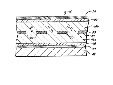
Referring now to Figure l, the transistor 40,
according the the present invention, is shown. Transistor 40
is a vertical thin film transistor formed of materials
deposited on a substrate 42, which substrate can be formed of a
wide variety of materials including glass. Deposited upon the
substrate 42 is a conductive layer of metal 44 which is used to
form one of the two current path electrodes of the transis~or
40. The metal layer 44 may be molybdenum, chrome, or aluminum
for example. Over the metal layer 44, a layer 46 of doped
amorphous silicon alloy, either n+-type or p~-type, is
deposited. On top of the layer 46, a layer 48 of substantially
intrinsic amorphous silicon alloy is deposited, which forms the
conduct~on channel or current path of the transistor 40. (For
convenience, layer 48 is often hereinafter referred to as t~e
i-a-S1, the intrinsic layer, or simply as the i layer.) A gate
layer 50, which may take the form of a grld, is located in the
i layer 48. In the embodiment of the invention shown in Figure
l, the gate layer 7s made of a ~aterial which forms a
rectifying junction with the semiconductor material of the
layer 48. The material of the gate 50 can comprise a metal,
such as platinum, which forms a Schottky barrier with the
intrinsic material of the layer 48, or it can be formed of a
doped semiconductor material which forms a rectifying
semiconductor junction with that material. The gate 50 is
formed as a layer containing openings 51 through which the
semiconductor material of layer 48 extends. Above the layer 48
a second layer 52 of doped amorphous silicon alloy is placed.
As is described below, this layer may be made of either n+ or
p material. Finally1 over the layer 52, a layer 54 of
conducting material, such as molybdenum, chromium or aluminum
metal, is deposited to form the second current path electrode
of the transistor.
The thicknesses of the various layers of transistor 40
can be ta110red to obtain desired electrical properties. The
metal electrode layers 44 and 54 should be thick enough to
provide eff1cient conduction to their associated ohmic contact
layers 46 and 52. For most uses a thickness of 500 to 3,000
angstroms should be sufficient. The ohmic contact layers 46
and 52 need be no thicker than 500 angstroms. The thickness of
-20-
879.1 ~L~ Z3
the ~ntrinsic layer 48 in general should be determined by a
trade-off between the increased current injection which results
from the layer 48 being thin, versus the increased ability to
withstand voltages caused by increasing the thickness of the
layer. Since intrinsic amorphous silicon alloys can withstand
approxlmately fifty volts per micron without semiconductor
breakdown, a device in which the layer 48 is one micron thick
will provide satisfactory operation for most low voltage
applications. The thickness of the gate layer 50 may be varied
in accordance with the desired operating characteristics of the
transistor 40. Preferably the gate should be thick enough that
its conductivity is sufficient to enable its various parts to
maintain a relatively uniform voltage (i.e., to ensure there is
no appreciable voltage drop within the gate layer itself). If
the gate is made of a conductive metal, a thickness of 20~ to
laO0 angstroms should be sufficient. If the gate layer is made
of a doped semiconductor material (without a metal core), the
gate layer may have to be somewhat thicker. The desired
geometry of the openings 51, especlally the width of the
openings, may also influence the thickness chosen for gate
layer 50. The openings 51 may thus range in size from a few
tenths of a micron to several microns.
Figure 2 shows a top view of one embodiment of gate 50
in which the openings 51 are formed as a plurality of parallel
slots. It is to be understood, however, that the openings 51
in this embodiment and most of the other embodiments may be
formed in other shapes, such as circular holes, and depending
on the application, may vary in number from one to many. Also,
in a number of applications the openings need not be of the
exact same size or uniformly spaced apart one from another.
They may even be positioned in a relatively random fashion in
the 9? te layer.
Preferably the amorphous silicon allsy of layers 46,
48 and 52 contain hydrogen and fluorine as density of states
reducing materials to improve their semiconductor properties.
The doped semiconductor layers 46 and 52 greatly improve the
ohmic nature of the contact between their associated current
path electrodes and the intrinsic material of layer 48. When
the material of layer 46 or 52 is doped to be n~ type, lt has
the characteristic of being able to in~ect many more electrons,
21~
879.1
or negative charge carriers, into intrinsic semiconductor
material than holes9 or positive charge carriers. On the other
hand, when the material of either of those contact layers is
doped to be p -type, 1t has just the opposite property, and
injects many more holes into intr1nslc sem1conductor material
than electrons.
Methods of depositing the materlals used to form
transistor 40 are well known in the art. Amorphous sil1con
alloys can be deposited in multiple layers over large area
10 substrates to form a multitude of circuits in high volume
continuous processing systems. These clrcuits may be designed
to employ many structures of the type shown in Figure 1.
Continuous processing systems for the fabrication of amorphous
siticon alloy circuit elements are disclosed, for example, in
U.S. Patent No. 4,400,409, issued August 23, 1983 and entitled
"A Method of Making P-Doped Silicon Films and Devices Made
Therefrom"~ U.S. Patent No. 4,542,711 issued September 24, 1985
for "Continuous Systems for ûepositing Amorphous Semiconductor
Material"; U.S. Patent No. 4,410,558, issued October 18, 1983
20 and entitled "Cuntinuous Amorphous Solar Ce11 Production
System"; IJ.S. Patent No. 4,438,723, issued March 27, 1984 and
entitled "Multiple Chamber Deposition and Isolation System and
Method"; and U.S. Patent l~o. 4,492,181 issued January 8, 1985
for "Method and Apparatus for Continuously Producing Tandem
Amorphous Photovol taic Cell s". As disclosed in these patents
a substrate may be
continuously advanced through a succession of deposition
chambers, whereln each chamber is dedicated to the deposition
of a specific material.
In making the layers 46, 48 and 52 shown in Figure I,
a single deposition chamber system can be used for batch
processing, or preferably, a multiple chamber system can be
used wherein a first chamber is used for depositing, for
example, a n -type amorphous silicon alloy for layer 46, a
second chamber is used for depositing an intrlnsic amorphous
sllicon alloy- for layer ~8, and a third chamber is used for
depos~ting an n+ or p~-type amorphous silicon alloy for
layer 52. Since each deposited alloy, and especially the
intrinsic alloy~ must be of rather high purityl the deposition
40 environment in the intrinsic deposition chamber is preferably
-22-
879.1 ~ ~ ~ 7 3 6'j
.
isola~ed from undesirable doping constituents within the other
chambers to prevent the dlffusion of doping constituents into
the intrinsic chamber. In the previously mentloned patents and
applications, wherein the systems are primarily concerned with
the productlon of photovoltaic cells, isolation between the
chambers is accomplished by gas gates through which
unidirectional gas flow is established and through which an
inert gas may be "swept" about the web of substrate material.
Deposition of the amorphous silicon alloy materials is
accomplished by glow discharge decomposition of process gases.
Among these processes, radio frequency energy glow discharge
processes have been found suitable for the continuous
production of amorphous semiconductors. An improYed process
for making amorphous semiconductor alloys and devices is
disclosed in U.S. Patent No. 4,517,Z23, issued May 14, 1~85 and
entitled "Method of Making Amorphous Semiconductor Alloys and
Devices Using Microwave Energy".
This process utilizes
microwave energy to decompose the reaction gases to cause the
deposition of improved amorphous semiconductor materlals. This
process provides substantially lncreased depos;tion rates and
reaction gas feed stock ut;1ization. Microwave glow discharge
processes can also be utilized in high volume mass production
of devices, as disclosed in U.S. Patent No. 4,515,107, issued
May 7, 1985, entitled "An Improved Apparatus for the
Manufacture of Photovoltaic Devices".
The gate 50 may be formed in the intrinsic
semiconductor layer 48 in the manner indicated in Flgure 3. As
is indicated in Flgure 3, a partial portion 48a of layer 48 is
deposited, and then a layer of material out of which the gate
50 is to be formed is deposited on top of the partial layer
48a. Then the gate layer 50 is patterned by convent;onal
photolithographic or electron beam techniques or the like so as
to create the openings 51. At this point the partially
completed translstor 40 has the appearance shown in Figure 3.
Then further deposition of the intrinsic amorphous silicon
alloy is performed on top of the gate 50, filling openings 51
and formlng partial portion 48b of 1ayer 48, so as to create
~40 the composite layer 48 7ndicated in Figure l.
-23-
879.l
As can be understood by those skilled in the art of
intergrated circuit fabrication, photolithographic techniques
can be used to provide electrical contact to the bottom
elestrode 44 at one location, to the gate e1ectrode 50 at a
second location, and to the top electrode 54 at a third
location. As can also be understood by those skilled in the
integrated circuit art, a plurality of transistors such as the
transistor 40 can be formed by photolithographic means on one
substrate and can be connected with each other and other
elec~ronic circuits components to create more complex
electronic circuitry.
Referring now to Figure 4A, a unipolar, or single
injection, embodiment 40a of the present invention is shnwn in
schemat;c form, with the substrate 42 and the metal layers 44
and 54 of the current path electrodes omitted to simplify the
Figure. In this single injection embodiment both of the doped
semiconductor layers 46 and 52, which form the ohmic contacts
for the two current path electrodes, are made of n
mater~al. As was stated above, n~ material ls efficient at
lnjecting electrons into intrinsic semiconductor material but
very inefficient at injecting holes into such material. As a
result, when one of the n~ electrodes is connected to the
negative terminal of a power supply and the other is connected
to positive terminal of a power supply, the current which tends
to result in the current path in the intrinsic semiconductor
material 48 between them is comprised almost exclusively of
electrons. Since this current consists substantially of charge
carriers of only one polarity, the device of Figure 4A is
properly called a unipolar device. When device 40a is
connected to a power supply PS as shown in Figure 4A, the
electron current (-ID) flows from current electrode 46, which
acts as the source (S), to current electrode 52, which acts as
a drain (D). It should be clear to those in the art that
transistor 40a may just as readily be connected to a voltage
source to make layer 46 the drain and layer 52 the source.
In the transistor 40a, the gate electrode 50, when
uninsulated, is preferably made of a material which forms a
rectifying junction with the intrinsic semiconductor ~aterial
of layer 48. Th~s rectifying junction helps prevent current
leakage from the gate electrode into the material of layer 48
- -2~
879.i ~b79~
when a voltage is applied to the gate to modulate current flow
through the transistor. In the $ransistor 40a, as was stated
above, both the current path electrodes have n~ ohmic
contacts and the current flow is comprised substantially only
of electrons. Thus the application of a negative voltage VG
to the gate 50 creates a barrier to the flow of electrons
through the opening 51 that tends to turn the transistor 40a
off. For this reason, the gate 50 of the transistor 40a is
preferably made of a metal such as a platinum or a
semiconductor material such as p+ doped amorphous silicon
alloy which forms a reverse biased junction with intrinsic
amorphous silicon alloy when it has or is giYen a potential or
voltage equal to or lower than that of the surrounding material
of layer 48. In this manner, the material of gate 50 forms a
small negative electric field E extending into the portion of
layer 48 which immediately surrounds it, thereby creating a
depletion region as is indicated in Fi~ure 4A by the dotted
lines 54. Figure 4B shows a qualitive graph of the magnitude
and extent of the fields EL and ER along the "x" direction
between two opposing left and right elements of the gate 50
when the potential of the gate is allowed to float. In Figures
5 through 9, qualitlve graphs of the electrical field intensity
EL and ER similar to that shown in Figure 4B are
superimposed between opposing elements of gate 50. As is shown
in Figure 5, in the absence of an applied voltage to the gate
50, the fields EL and ER extend onlg partially across the
opening 51, and thus do not substantially bar the flow ~f
electrons across the channel 51 of transistor 40a. As is shown
in Figure 6, however, as the voltage applied to the gate 50
relative to the intrinsic material of layer 48 which surrounds
it is increased, the fields EL and ER which extend across
the opening 51 increase, so that a much laryer portion of the
opening 51 has a net negative field which tends to repel the
flow of electrons across it. This effectively narrows the size
of opening 51 to electrons and decreases the current flowing
between the contacts 46 and 52. As is shown ln Figure 7, if
the negative voltage applied to the electrodes 50 is lncreased
even further, the combined negative field of EL and ER will
extend all the way across the opening 51, so as to
substantially cut off the flow of electrons in the current path
-25-
.. .
879.l ~ 9~
of the transistor 40a.
It should be clear from the foregoing description of
transistor 40a that the application of an appropriate biasing
voltage to gate 50 will tend to turn transistor 4~a off, and
that the absence of such a biasing voltage on gate 50 allows
transistor 40a to be on. It ~s possible, however, to fabricate
a transistor similar to transistor 40a which is off in the
absence of an applied voltage, and which turns on with the
application of a positive gate voltage. Th~s can be done by
making the opening between the gate elements 50 very narrow, as
is indicated schematically in Figures 8 and 9, and by selecting
the material of the gate 50 so that the depletion region in the
intrinsic material which surrounds the gate extends all the way
across the openings between its elements in the absence of an
applied voltage, as is indicated in Figure 8. In such a
device, electron flow through the opening 51 will be
substantially prevented in the absence of an applied gate
voltage. However, if a positive voltage is applied to the gate
50, the wldth of the depletion region surrounding the gate will
be decreased, as is indicated in Figure 9, and the barrier to
electron flow through the opening 51 will be reduced, thereby
increasing current through the transistor containing such a
gate. To prevent current conduction between the gate 50 and
the current-carrying electrodes 46 and 52, especially when the
gate is forward-biased with respect to either current-carrying
electrode. The gate is preferably substantially or co~pletely
insulated as will be further described in conjunction with the
embodiments of Figures 15 and 18.
In the discussion above, the unipolar transistor 40a
has two n+ ohmic contact layers 46 and 52 and has
substantially only electrons as the current carriers. It
should be understood, however, that a unipolar device of the
opposite polarity can be created by fabricating a similar
transistor in which both of the current path electrodes have
p~ ohmic contact layers. In such an embodiment of the
present invention, the gate 50 is formed of a material which
tends to form a depletion region in the surrounding portion of
the layer 48. In such a device the p+ layer supplied with a
relatively pos~tive voltage tends to lnject only holes into the
semiconductor material of the layer 48, ~nd thus the current
-26-
879.l ~ 6~
flow consists substantially only of positive charge carriers.
In such a devlce, the application of a positive vol~age to the
gate 50 would tend to increase the extent and magnitude of a
positive field generated by the gate, causing that field to
extend across the one or more openings 51, creating a barrier
to the flow of holes through those openings, and thus tending
to reduce the current flow across such a transistor.
Figure lOA shows another embodiment of the present
invention. The transistor 40b shown in Figure lOA is
substantially identical to the transistor 40a shown in Figure
4A except that its top ohmic layer 52 is formed of a p~
semiconductor material rather than the n+ semiconductor
material shown in Figure 4A. This small difference in
construction results in a substantial change in operation. It
causes the current flowlng in the transistor 40b to be
ambipolar, that is, comprised of carriers of both polarities,
i.e., both holes and electrons, rather than iust carriers of
one polarity, as is the case with regard to the transistor
40a. This difference results from the fact that the p+
material of layer 52 ln Figure 10 tends to inject holes into
the intrinsic material of layer 4~ when it is supplied with a
positlve voltage relative to layer 48. Thus, when the
translstor 40b is electrically connected as indicated in Figure
llA with the n~ layer 46 connected to a relatively negative
voltage and the p~ layer 52 connected to a relatively
positive voltage, the layer 46 (which may be called the
cathode) injects electrons into the intrinsic layer 48 which
are attracted towards the positive voltage on layer 52, and the
layer 52 (which may be called the anode) injects holes into the
layer 48 which are attracted towards the negative voltage on
layer 46. Because both electrons and holes are injected into
its layer 48, the transistor 40b is also referred to as a
double injection device. In such devices, it is preferable to
insulate the gate 50 to m~nimize conduction through the gate to
e1ther of the current-carrying electrodes 46 or 52.
The ambipolar, or double injection, nature of
transistor 40b provides a very important advantage over the
unipolar transistor of Flgure l: it enables significantly
larger currents to flow. Although the amount of current which
flows in both single and double injection devices depends on
-27-
879,1 ~7~
. .. ~ ~; .
many variables, such as temperature, thickness o~ the
semiconductor current path, and applied voltage, it is easily
possible for ambipolar devices to have on currents a thousand
times greater than those obtained by similar single injection
devices under the same operating c~nditions. This is
illustrated by Figure lOB, which shows experimentally produced
current dens~ty versus voltage (anode to cathode) curves of
similar single injection (n-i-n) and double injection (p-i-n~
a-Si alloy diodes at 25C. M. Hack, et al., "A Comparision
lo of S1ngle And Double-Carrier Injection In Amorphous Silicon
Alloys", Journal of Applied Physics, Vol. 58, pp. 1554-1561
(1985), presents results from both experimental and theoretical
studies which explain in detail the mechanisms of single and
double inject~on in unipolar and ambipolar diodes formed from
such alloys, including the curves shown in Figure llB.
The reason an ambipolar device makes such an increase
ln current possible may be explained as follows, In the
unlpolar device of the type shown in Figure 4A substantially
all of the conduction is performed by charge carriers of one
polarlty, such as electrons. As more electrons are injected
into the current path of the unipolar transistor, the negative
space charge created by excess electrons in the intrinsic 1ayer
48 tends to retard the injection of further electrons, and thus
tends to limit the rate at which current may increase in
proportion to increases in applied voltage between the top and
bottom electrodes. Thls effect is known in the art as space
charge limited conduction, However, in an ambipolar device an
increase in voltage between the top and bottom electrodes
causes an increased number of charge carriers of both
polarities to be injected into its current path, and thus there
tends to be a very much smaller increase in space charge caused
by an increase ln charge carriers, since the positively charged
holes tend to cancel the space charge caused by the ne~atively
charged electrons. The 1ncrease ln the number of charge
carrlers made possible by double inject~on makes amb~polar
devices capable of handling much larger currents than single
injection devices for the same bias. In addition, the
increased number of charye carr1ers made possible by double
-2~-
-- 879.~
injection tends to fill a high percent o~ the traps or defect
states which occur in amorphous silicon alloys at energies in
the forbidden gap, increasing the drift mobility of both
electrons and holes and thus further increasing the
conductivity of double injection transistors.
The foregoing results of ambipolar operation may be
explained in slightly more theoretical terms as follows. In
both amorphous and crystalline semiconductor materials,
electron band mobility is known to exceed hole band mobility.
Accordingly, n-p-n bipolar transistors and n-channel MOSFETs
may generally have a greater current capability while operating
at a given bias voltage than do corresponding p-n-p bipolar
transistors and p-channel MOSFETs. In the p-i-n transistor 40b
of the present invention described above, the net space charge,
defined as the excess of electrons over holes per unit volume
of intrinsic semiconductor material in the conduction channel,
still operates to limit channel conduction, but at much higher
current levels than are possible in a similarly constructed
unipolar FET. When the p-l-n transistor is turned on by
application of a suitable gate voltage (or allowing the gate to
float), a current path or channel, whlch extends in a generally
vertical direction through the lntrinsic material above and
below the gate layer, is formed. The channel may, for example,
narrow to fit through the channel opening(s) and flare
outwardly therefrom above and below in an hourglass shape.
Both electrons and holes begin to move or flow in the channel
on account of the electric field created by the anode-cathode
voltage. The number of electrons throughout most of the
channel is greater than the number of holes, due to the
superior band mobility of the electrons as well as the
asy~metrical density of states distribution in the band gap of
undoped a-Si material. For convenience, then, electrons may be
called the primary or dominant charge carriers, and holes may
be called the neutralizing or compensating charge carriers.
(This condition can also be reversed, as will be explained in
greater detail later.) The forward bias at the p-i junction at
the boundary between layers 52 and 48 reduces the barrier
height at the junction, allowing more holes to diffuse into the
intrinsic channel from the p+ current path electrode. (The
forward bias at the i-n junction between layers 48 and 46
-29-
879.1 ~ 3~
similarly allows more electrons to diffuse ;nto the intrinsicchannel from the n current path electrode 46.) Once in the
intrinsic channel, the holes, upon application of forward bias,
tend to be drawn toward the negatively biased current electrode
due to the over-all field in the channel. The additional holes
or compensating carriers tend to neutralize the space charge
due to excess electrons or primary carriers in the channel,
which allows even more electrons to enter the channel. The
~oregoing process continues until other mechanisms, perhaps
such as hole mobility or the rate at which the p+ layer 52 is
able to e~ficiently inject holes into the intrinsic layer 48,
lim1t the number of holes which can be simultaneously present
with electrons in the channel. As that equilibrium point is
reached, the number of excess electrons levels off due to the
net space charge creating space charge limited conduction. The
significance of the double inject~on process over single
injection may be more forcefully presented by the following
simplistic illustration. Let us assume that on account of
space charge limited conduction, the maximum net charge per
unit volume throughout most of the channel region adjacent the
insulated gate is ten carriers for a specified gate voltage.
Thus, in a unipolar system operating under these assumptions,
the maximum the number of carriers contributing to conduction
per unit volume cannot exceed ten carriers. However, in an
ambipolar system operating under these assumptions and having
the same mobilities, the maximum number of carriers may be, for
example, 1,010 primary carriers and 1,0~0 neutralizing
carriers, resulting in 2,01a carriers contributing to
conduction per unit volume. Note that the net space charge is
st111 ten carriers (1010 - 100~ - 10). Accordingly, in this
lllustration, the current in the ambipolar system is 201 times
higher than the current of the unipolar system for the same
mobil~ties.
Those in the art should appreciate that the teachings
of the present invention can be appl~ed to create ambipolar
devices having holes as the dominant charge carrier and
electrons as the compensating charge carrier. This is done,
for example, in VMITs which operate by stopping the ftow of the
holes through the opening in their gates, which greatly0 diminishes the flow of electrons through the opening as
-30-
879.1 ~ ~ ~ 7~3~ ~
previously explained. Our computer modeling indicates (or atleast suggests) that in the operation of an ambipolar device of
the present invention, the dominant carriers are controlled
directly by the voltage applied to the gate, and the
compensating carriers are cGntrolled indirectly by the voltage
applied to the gate, in that the compensating carriers are
primarily responding to the current and space charge density
fluctuations of the primary carriers~ In other words, a gate
voltage of one polarity controls charge carriers of both
polarities. Other exemplary embodiments of the present
invention having holes as th~ dominant charge carrier are shown
in Figures 39 and 40.
Our computer modeling for a-Si al10y ambipolar devices
of the present lnvent10n also indicates that in general the
holes are distributed relatively uniformly throughout the
conduction channel, and that the recombination of holes and
electrons occurring in the conduction channel consumes most, if
not all, holes injected into the intrinsic material by the p+
current path electrode. It shows that a heavy concentration of
majority carriers very near the i-n junction ~l.e., electrons)
consumes any holes which may have travelled that far, or which
are created near the vicinity of the i-n junction. There may
be other localized perturbations to the generally uniform
distribution of holes, such as at the p-i junction or at the
interface or boundary between the insulated gate and intrinsic
semiconductor region. When the intrinsic material is an
amorphous semiconductor, such as an alloy of silicon, the
greatly increased number of holes and electrons is believed to
fill many or most of the defect states or traps in the
materlal, thus allowing more of the injected electrons to go
into the conduction band and the injected holes to go into the
valence band. This trap-filling phenomenon pushes the electron
quasi Ferml level further toward the conduction band and the
hole quasi-Fermi level further ~oward the valence band than is
possible in a comparable unipolar system. The phenomenon
should also split the quasi-Fermi levels in semiconductor
material, such as polycrystalline material, which does not have
nearly as many defect states as amorphous material. This
process leads to ambipolar devices having increased current0 flow for any given channel depth as compared to unipolar
-31-
~- 879.1 ~ ~ ~;
current flow.
In any semiconductor electrons and holes can recombine
both radiatively and non-radiatively. When the quasi-Fermi
livels are split by an energy approximately equal to the band
gap of the material, a significant amount of the carr~er
recombination will be radiative and hence the device will
exhibit electroluminescence, Yet another advantage of the
trap-filling phenomenon ~s that it is possible to construct
ambipolar transistor devices of the present invention from
amorphous silicon alloys which exhibit electroluminescence.
When the injection levels become sufficiently high so that the
difference between the quasi-Fermi levels becomes comparable to
or greater than the energy gap, then light emission, and, with
the 1ncorporation of a suitable optical cavity, coherent light
emission (i.e., lasing) may occur as will be explained in
greater detail later with respect to Figures 39 and 40.
One more significant advantage of the ambipolar
operation is that wider conduction paths or channels can be
achieved for a given gate voltage than is possible with the
n-i-n or p-i-p transistor devices on account of neutra1ization
of space charge. This enables higher current for a1most any
given transistor geometry. This advantage will be explained in
more detail in conjunction with the horizontal ambipolar
embodiments shown in Figures 29A and 36.
The expected current-Yoltage curve of the transistor
40b is shown in Figure llB. As indicated in Figure llA, which
is a schematic diagram of another version of transistor 40b
similar to that shown in Figure lOA, there is a voltage drop
across the intrinsic layer 48. The voltage drop within the
layer 48 ~s generally nonlinear with respect to distance
between the current path electrodes and varies with the amount
of current flowing therethrough. For the purposes of the
following discussion, however, we will assume a relatively
linear voltage drop through layer 48. This voltage drop causes
the voltage of the material of layer 48 to range fro~
approximately zero volts at the portion of that layer which
touches the n~ layer or cathode 46 to approximately five
volts at the por~ion of the layer which touches the p~ layer
or anode 52. If the gate 50 is located approximately midway
through the layer 48, the voltage of the intrinsic material
-32-
879.1
with which it ~s in contact, based on the assumption oflinearity, will be appro~ima~ely 2.5 volts. The gate 50, if
allowed to float9 will be at approximately that voltage. As is
shown in Figure llB, the current flowing through the transistor
has its maximum value when the gate 50 ls at approximately 2.5
voltsO If a voltage is applied to the gate 50 which is lower
than this floating potential, the gate tends to, depending on
the applied gate voltage, more weakly attract or even repel
electrons, which tends to decrease the flow of electrons
through the opening between its gate elements~ Preliminary
experimental results suggest that the application of a voltage
below the floating potential of the gate decreases not only the
flow of electrons through the openings in the gate, but also
decreases the flow of holes, alkhough the decrease in the flow
of holes is somewhat less than the decrease in the flow of
electrons. This decrease in the flow of holes is caused by the
tendency to maintain space charge neutrality. Similarly, if a
voltage is applied to the gate 50 which is above the gate's
floating potential, the positive f1eld induced at the gate may
tend to initially 1ncrease the flow of electrons ~and by
compensation, holes) through its openings 51. However, the
reduction in electric potential between the gate electrode and
the anode electrode reduces the device current, as shortly will
be further explained. The graph of Figure llB ~llustrates in a
general way how the anode current IA may vary as a function
of gate voltage VG in the field effect transistor device 40b
of Figure llA. As will also be explained, a number of factors
will ~nfluence preclse shape of this curve.
The most likely explanation-for why the application of
a voltage to gate 50 which more weakly attracts or repels
carriers of one polarity also repels carriers of the opposite
polarity or at least reduces their number is as follows.
Energy considerations create a strong preference for space
charge neutrality throughout the current path between the
electrodes 46 and 52. If a voltage is supplied to the gate 50
which tends to keep charge carriers of one polarity out of the
opening 51, the tendency toward space charge neutrality tends
to greatly reduce the presence of charge carriers of an
opposite polarity in that opening since there is a limit to
overall nek charge that can be contained in any given volume.
-33-
~- 879.1 ~ ~ ~ 7 ~ ~ ~
The floating potential of the gate 50 in the Figure
llB transistor is a function of the voltage drop across the
thickness of the layer 48 between the positive and negative
potentials of fiYe and zero volts, respectively, applied to
contacts 52 and 46. If, as is shown in Figure 12A, the gate 50
is placed nearer the p+ layer 52 than the n layer 46, the
gate will tend to float at a voltage which is nearer five volts
than zero voltsO Assuming for purposes of example that the
gate in Figure 12A floats at approximately four volts, then the
anode current IA f the Figure 12 device should vary with
applied gate vo1tage VG roughly as shown in Figure 12B, and
should reach its peak at a gate voltage of approximately four
volts, as shown. On the other hand, if the gate 50 is placed
substantially closer to the n contact 46 than to the p+
contact 52, as is shown in Figure 13A, the gate 50 will tend to
float at a voltage which is substantially closer to zero volts
than five volts. Assuming for purposes of example that the
gate 50 in Figure 13A is placed in a position so that it ~loats
at approxlmately one volt, then the current-voltage curve of
the resulting device, should be roughly as is shown in Flgure
13B, and will tend to reach its maximum current at a gate
voltage of approximately one volt, as shown.
The current-voltage curves of Figures llB, 12B and 13B
show that by controlling the position of the gate 50 relative
to the current electrodes 46 and 52, it is possible to greatly
alter the current-voltage characteristic of a device of the
general type shown in Figure lOA. The current-voltage curve
shown in Figure llB is that of a device which is substantially
off when the voltage of either of its two current path
electrodes is applied to its gate, but which is turned on to a
maximal current flow when the gate is supplied with a suitable
intermediate voltage, or is allowed to float. The
current-voltage curve shown in Figure 12B is that o~ a device
which is substantîally on when ~ts gate ls supplied with a
voltage close to that of its higher voltage current path
electrode (anode), but is substantially off if its gate is
supplied with the voltage close to that of its lower voltage
current path electrode (cathode), The current-voltage curve
shown in Figure 13B is just the opposite, since it is that of a
device which is substantially on when its gate is supplied with
-34-
879.1 ~i796~
the voltage close to that of its lower voltage current path
electrode, and is substantially off when its gate is supplied
with the voltage close to that of its higher voltage current
path electrode~
Figures 14A and 14B i11ustrate how the current-voltage
curve of the ambipolar device of the present invention can be
tailored in another significant way. The width of that portion
of the curve in which the transistor is substantially on can be
narrowed or widened as a function of the width of the openings
51 between thP elements of its gate SO. If the openings 51 are
narrowed, smaller voltages between the gate and its surrounding
intrinsic semiconductor material are capable of generatlng an
electric field of sufficient strength to substantially stop
current flow all the way across the openings 51, and thus
substantially turn the transistor off. This greater
sensitiv~ty to gate voltages is shown in Figure 14B. On the
other hand, if the gate openings 51 are widened, much stronger
(i.e., more posi~ive or negative) voltages must be applied to
the gate relative to the surrounding intrinsic material in
order to generate a field of sufficient strength to
substantially limit current flow all the way across the
openings 51. ~hus in a transistor with such widened openings
51, the sensitivity of the device to changes in gate voltages
will be decreased.
It should be understood that the current-voltage
diagrams shown in Figures llB, 12B, 13B and 14B are logarithmic
in their vertical direction, and that the change in current
flow between a transistor 40b which is on and which is off may
vary by several orders of magnitude depending upon device
geometry. It should also be understood that these diagrams are
only approximate, since the actual shape and position of such
curves depends upon many factors. For example, one very
important factor is the size of the opening(s) 51. Another is
the th~cknesses of the upper intrinsic layer 48a and the lower
intrinsic layer 48b. Also, in transistors of the present
invention in which the gates are made of a material which
creates a depletion region in neighboring intrinsic material in
the absence of an applied voltage, the current-voltage curve
will tend to be shifted to either the right or the left by the
presence of such a self-generating field across the openings
-35-
~79.1
51. In addition, since the mobility of electrons and holes are
not identlcal, the current-voltage diagram is not symmetrical
about its point of maximum current. The current-voltage curve
also tends to be asymmetrical because the number of defect
states in amorphous silicon alloy at energies close to the
conduction band, in which electrons are trapped, is different
than (i.e~, lower than) the number of defect states at energies
close the the valence band, in which holes are trapped~ The
thickness of the gate layer 50 relative to the size of the
openings 51 can also be an important factor, since it
influences the shape of the electric field induced by a voltage
applied to the gate. In addltion, the relative strength of the
voltage applied across the current path electrodes 46 and 52
has a bearlng upon the resultant current-voltage curve.
In both the unipolar and ambipolar embodiments of the
invention where it is desired that the transiskor have a high
current capacity, the semiconductor material of the current
path should be selected to provide relatively long carrier
lifetimes. When the current path is made of amorphous silicon
alloy, this normally means the current path should be made of
intrinsic amorphous silicon alloy, since such intrinsic
material has far less defect states than doped amorphous
silicon alloys. In certain ambipolar embodiments of the
transistor of the invention where it is desirable to turn off
the transistor rapidly, certain elements may be mixed in with
the amorphous silicon alloy of the current path to reduce
carrier lifetimes. For example, materials such as gold may be
mixed into the silicon alloy to create recombination centers
having energy levels approximately half way between the
energies of the conduct~on and valence bands. The benefit of
such recombination centers is that they greatly increase the
rate at which holes and electrons recombine in the current
path, and thus they shorten the length o~ time it takes the
current path to be cleared of carriers when the transistor is
turned off.
Figures 12A and 13A show that the gate 50 may be
asymmetrically placed with regard to the two current path
contacts 46 and 52 to shift the current-voltage curve. In
certain ambipolar embodiments of the invention, however,
there is another reason for asymmetrical placement of the gate
-36-
- 879.1
50 with regard to the contacts 46 and 52. This reason relates
to the reduction of leakage current. In ambipolar embodiments
of the invention in which the gate 50 is made of an n+ or
p+ material that forms a rectifying junction with the
material of the current path, unacceptable levels of current
will tend to leak from the planar surfaces of the gate unless
its junction with the current path is reverse biased. If the
planar surfaces of the gate covers a relatively large area,
such gate leakage current could be substantial even though the
gate leakage current density is relatively l~w. If, however,
the gate is supplied with a voltage between that of the two
current path electrodes 46 and 52, as is described above with
regard to Figures 12B through 14B, the gate will be forward
biased with regard to both the anode and the cathode, which
creates substantial and undesirable currents between both
current-carrying electrodes 46 and 52 and the gate 50.
Accordingly, it is highly recommended that the gate 50 be
almost fully or ~ully insulated for those amblpolar embodiments
of the ~nvention to be operated with gate voltages between that
of the two current path electrodes 46 and 52.
The leakage current between the gate 50 and the
current path electrode 46 or 52 which has the same conductivity
type as the gate is unipolar due to single injection. Such a
single injection gate current path (for voltages greater than
about 0.7 volts) normally conducts substantially less current
than does a double injection current path between the gate and
the current path electrode of the opposite conductivity type.
These facts may be utilized to minimize overall gate leakage
current to or from both of the planar surfaces of the gate in
the following ways~ First, the transistor may be operated in a
voltage range in which the gate is reverse biased with regard
to the electrode with which it forms the double injection
leakage path, and forward biased with regard to the electrode
with which it forms the single injection gate current path.
This substantially shuts off leakage current in the more
conductive double 1njection gate leakage path, and limits it to
the less conductive single injection gate leakage path.
Second, asymrnetrical placement of the gate 50 allows the single
injection leakage current to be reduced even further, i.e., the
gate is placed so the single injection gate leakage path is
-37-
879.1
longer than the double injection gate leakage path. Such
shortening of the double injection gate leakage path has little
adverse effect on double injection gate leakage current, which
is virtually zero due to the aforementioned reverse bias. But
the lengthening of the forward biased single injection gate
leakage path substantially reduces gate leakage current~ since
the conductivity of a single injection curren~ path decreases
rapidly with lncreasing leakage path length.
The devices in all of the embodiments of the invention
discussed in detail above which do not include an insulating
layer around the gate rely upon depletion regions formed
between the gate 5Q and the intrinsic material of layer 48 to
prevent or reduce the leakage current from the gate into the
layer 48, and through that layer to the translstor's current
path electrodes. Although such depletion regions do
significantly reduce leakage current, experiments have
indicated that substantially increased performance can be
obtained by insulating as much of the surface of the gate 50
from the layer 48 as possible.
Referring now to F~gure 15, the transistor 60 therein
shown is substantially identical to the transistor 40 shown in
Figure 1 except that the bottom of its gate 50 is insulated
from the lower portion 48a of intrinsic material 48 by a bottom
insulating layer 62 and the top of its gate 5Q is insulated
from the upper portion 48b of layer 48 by a top insulating
layer 64. Such a device may be readily fabricated in the
manner indicated in Figures 16 and 17.
Figure 16 shows the transistor 60 in a partially
constructed state in which the bottom current path electrode 44
and its nl ohmic contact 46 have been deposited upon the
substrate 42 and have been covered by the bottom portion 48a of
the ~ntrinsic layer 48. On top of the layer 48a the bottom
insulating layer 62 has been deposited. The conductive
material of the gate 50 has been deposited upon the layer 62.
Finally, the top insulating layer 64 has been deposited on top
of the gate layer 50. Preferably, the layers 62 and 64 are
formed of deposited insulating material such as silicon oxide
(sixoyj or sllicon nitride (SiXNy)~ Preferably, each
of these insulating layers ~s between 200 and 5,000 angstroms0 thick. A layer 66 of photoresist is deposited upon the top
-38-
- 879 1
insulating layer 64 and is patterned by exposure to actinic
radiation through a patterning mask and by subsequent
development. After the photoresist 66 has been patterned, the
partially completed transistor 60 has the appearance shown in
Figure 16. Then the structure is submitted to a plasma etch,
such as an NF3 etch or a CF4 and 2 etch, which removes
the portlon of the insulating layer 64 exposed through the
openings in the photoresist layer 66. The structure is next
submitted to an acid or plasma etch of a type known in the art
(such as a CHC13 etch) to remove the metal material of the
layer 50, so as to form the openings 51. Preferably the
structure should be submitted to this etch for a sufficient
length of time to cause some undercutting in the layer 50
(indicated by dotted lines 50u in Figures 15 and 17) so that
upon the next deposition of intrinsic semiconductor material to
fill openings 51 and form the top portion 48a of layer 48, the
intrinsic material will not contact the gate 50, thus reducing
leakage at the uninsulated edges of the layer 50 which define
the openings 51. After the portions of the layer 50 which are
not covered by the photoresist 66 have been removed by such an
etch, the structure ~s submitted to another etch, such as an
NF3 etch, to remove the insulating material of layer 62 that
: is exposed through the openings in the photoresist 66. Care
should be taken in performing this final etch, since most
etchants that will remove materials such as silicon oxide and
silicon-nitride used in layer 62 will also tend to etch
amorphous silicon alloys of the type used in layer 48a. Thus
this final etch step should be timed so as to allow the entire
exposed portion of layer 62 to be removed, while minimizing the
amount of subjacent intrinsic layer 48a which is also removed.
Once this final etch has been completed, the partially
constructed transistor 60 has the structure shown in Figure
17. At this point the photoresist layer 66 is removed, and
then a second deposition of intrinsic silicon alloy is
performed, so as to create the upper portion 48b of the layer
48. After this has been done, the n~ or p~ layer 52 and
the metal electrode 54 are formed in the manner described above
with regard to Figure 1.
As was stated above, the structure sho~n in Figure 15
has markedly less leakage current between its gate electrode
-: -39-
8 7 9 ~ ~ r ~
and its current path electrodes than the previously shown
embodiments of the invention. The previously mentioned
undercutting of the metal of its gate layer 50 should make it
possible to substantially avoid electrical contact between the
gate 50 and the layer 48. Figure 18A shows another way to
virtually eliminate the leakage current from the gate electrode
SOO In the Figure 18A device 70, the electrode 50 is made
smaller in horizontal extent than either the top or bottom
insulating layers 62 and 64, and thus it is totally
electrically insulated ~y them. As can be understood by those
skilled in the photolithographic art, such a structure is made
by depositing the layer 62 upon the top surface of the layer
48a, which top surface is indicated in Figure 18 by the dotted
line 489. Then the gate layer 50 is formed upon the insulating
1ayer 62 and is patterned via photolithographic techniques~
Then the top insulating layer 64 is formed as a continuous
layer over the patterned gate 50. After the deposition of the
insulating layer 64, photol~thographic techniques are used to
etch through portions of the layers 64 and 62 located between
the fingers of the gate 50. The photolithographic process is
designed, however, so that portions of the 1ayer 64 which cover
the top and side surfaces of the layer 50 are not removed.
Then the top portion 48b of the intrinsic layer 48 is deposited
in the manner described above, followed by the ohmic layer 52
and the electrode layer 54.
Referring now to Figure l9A, a transistor 80 according
to an alternate higher speed embodiment of the invention is
shown. The transistor 80 is somewhat similar to the transistor
60 shown in Figure 15, but the insulating layers 62 and 64
above and below its gate electrodes are much thicker, and the
intrinsic semiconductor material 48, instead of surrounding the
gate electrode 50, as is shown in Figure 15, instead is only
deposited ~n openings between the gate electrodes in the
transistor 80. The benefits of the transistor 80 include
reduced leakage from its gate electrodes due to the thicker
insulator layers, and reduced eapacitance between its
electrodes since the relative permittivity of the insulator
layers is higher than that of the intrinsic amorphous silicon
alloy of layer 48. Reduced capacitance is important, since it0 increases the speed of operation of such a translstor. In
-40-
879.l ~ 6 ~
;: addition, the greater distance between the top electrode 54 andthe gate 50, due to the thickness of the layer 48 which
overlies the gate 50~ results in a further reduction in
capacitance in the transistor 80, thus increasing speed of
operation.
As is shown in Figures 20 and 21, the transistor 80 is
constructed by depositing a plurality of layers of different
material upon the substrate 42, etching through a group of
those layers to create the structure shown in Figure 21, and
then depositin~ the intrinsic layer 48 and the top ohmic and
electrode layers 52 and 54.
Before the etching steps take place, the bottom
current path electrode layer 44, preferably made of a
conductive metal such as chrome or molybdenum and preferably
1,000 to 5,000 angstroms thick, is deposited. On top of that a
layer 46 of n+ material is deposited for purposes of making
an electron injecting ohmic contact. This layer is preferably
approximately 500 angstroms thick. On top of the layer 46 a
thin layer 82 of aluminum or molybdenum is depos~ted preferably
2~ about 500 angstroms th~ck. As is described below, this layer
functions as an etch stop or end puint detector. Over the
metal layer 82 a relatively thick layer of insulating material
62 is deposited. Preferably layer 62 is made of a deposited
insulator such as silicon oxide or silicon nitride. The
preferred thickness for the layer is between 200 and 5,000
angstroms. Next a layer of metal preferably about 200 to l,OOO
angstroms thick is deposited to form the gate layer 50. A
plurality of different metals can be used for this purpose,
including chromium and molybdenum. Above the layer 50, an
insulating layer 64 is deposited, preferably made of the same
material and of the same thic~ness as the layer 62. Once all
o~ these layers have been deposited, a layer of photoresist 84
is deposited on top of the layer 64 and is patterned by
exposure and subsequent development, so as to create a
patterned etch mask as is shown in Figure 20.
After the photoresist layer 84 has been patterned, the
entire structure shown in Figure 20 may be submitted to a
plurality of etches so as to etch through the layers 64, 50,
62, and 82 and thus produce the structure shown in Figure 21.
An etch, such as an NF3 etch or a CF4 and 2 plasma etch,
-41-
879.~ 796~
is used to remove the portion of the top insulating layer 64
which is exposed through the photoresist mask 84. Then the
structure is submitted to an acid or plasma etch of a type
designed to remove the metal material of layer 50 exposed by
the photoresist mask 84. After that, the structure is
submitted to another NF3 etch or CF~ and 2 etch to
remove the insulating material in layer 62 exposed by the mask
84. This etches the layer 62 down to the metal layer 82, which
is either an etch stop or the end point indicator for a laser
detection system. An etch stop is necessary with an NF3
etch, and most other etches which are effective in removing
materials such as silicon nitride, since they also tend to be
effective etchants against amorphous silicon alloys. After the
exposed portion of the bottom insulating layer 62 has been
removed, the structure is submitted to a second acid or plasma
etch of a type which removes the exposed portions of the metal
in the layer 82.
When layers 50 and 82 are made of a suitable metal,
such as molybdenum, a suitable plasma etch such as a CF4 and
2 etch, may be used to remove the insulating layers 62 and
64 and the metal layers 50 and 82 in one continuous etching
step. A laser end point detection system may be employed
during such a step to monitor the progress of the etching. As
~s known in the art, such a detection system works by
illuminating the layered structure to be etched with the laser
and then monitoring the changing reflectivity due to
interference as the etchant successively exposes each
underlying layer. The reflectivity increases as each
molybdenum layer is encountered and decreases when an
intrinsic, n~, p~ or insulating layer is encountered.
Accordingly, the drop in reflectivity immediately subsequent to
the second rise in reflectivity indicates that the etching has
reached layer 46, and therefore should be stopped. After
completing the foregoing processing steps, the partially
constructed translstor 80 has the structure shown in Figure 21,
in which a complete opening has been made through the
multilayered structure formed by layers 64, 50, 62 and 82 in
the gaps 51 between the gate elements 50, and in which the n~
layer 46 of the bottom electrode is exposed in each of these
openings.
-42-
879,l ~2~7~
Once this has been done, the photoreslst layer 84 is
removed and a layer 48 of substantially intrinsic amorphous
silicon alloy is deposited, as shown in Figure l9A. It is
important to remove the photoresist layer 84 before depositing
the semiconductor layer 48, because otherwise the organic
compounds in the photoresist may contaminate th~ layer 48 and
severely damage its electronic properties. The thickness of
the layer 43 deposited should be sufficient to fill the
openings formed in the multilayered structure formed of layers
64, 50, 62 and 82. Once layer 48 has been deposited, a layer
52 of doped amorphous s~licon alloy is deposited having a
thickness of approximately 500 angstroms. Then on top of the
layer 52 a layer 54 of metal, such as chromium, molybdenum or
aluminum, preferably having a thickness of 300 to 5,000
angstroms, is deposited to form the top current path electrode.
Preferably the etching steps in which the metal of
layer 50 and the metal of layer 82 are removed are allowed to
continue sufficiently long so that the metal in the layer 50 is
sufficiently undercut, as ls indicated 1n dotted lines 50u in
Figures l9A and 21, so as to reduce the likelihood of contact
between the conductive metal of layer 50 and the deposited
intrinsic amorphous semiconductor of layer 48. If this is done
the gate electrode 50 should be substantially electrically
isolated from the layer 48, thus reducing leakage current from
the gate almost to zero.
As was stated above, one of the maior advantages of
the transistor 80 is its low capacitance. The c~pacitance of
this transistor can be reduced even further if the bottom
electrode comprising layers 44, 46 and 82 are patterned before
the deposition of layer 62 so as to not cover the portion of
the substrate 42 wh1ch is to be covered by the gate elements
50. Similarly the top electrode comprised of layers 52 and 54
may also be patterned by photolithograph1c means so as not to
cover the portions of the translstor 80 aboYe the gate elements
50. Such a removal of the top and bottom electrodes from the
portions of the transistor in which the gate elements 50 are
located will substantially further reduce the capacitance
between the current path electrodes and between the current
path electrodes and the gate, thus increasing the speed of the
transistor. Also, by using ion milling or other suitable
-43-
879.l ~ X ~ ~ 9~ ~
techniques, the portions 48d of layer 48 above the top
insulating layer 64 may be removed so as to have the intrinsic
material and current conducting path therethrough substantially
confined to the openings in the layers 62, 50 and 64. Finally,
transistor 80 may, if desired, be constructed with a single
openin~, rather than the plurality of openings lndicated in
Figure l9A.
The transistor 80a shown in Figure l9B is an example
of a transistor structure which is basically constructed like
transistor 80, but which incorporates the last two
suggestions. Note that transistor 80a advantageously provides
a planar top surface upon which further layered structures or
elements may be deposited or otherwise formed.
Although the transistor 80 can be constructed to be
unipolar by having the ohmic contact layers 46 and 52 be doped
to have the same conductivity type, such as n+ conductivity
type, it is preferred that one of the ohmic contact layers be
n+ and the other be p~, so that the transistor ~0 wi~l be
an ambipolar device in which current conduction is performed by
both holes and electrons. As is described above, such an
ambipolar device has the great advantage of a much greater
current flow. Such an increase in current flow not only
results in the ability of the transistor to handle more power,
but also tends to increase the speed of the transistor by
reducing the time required to charge and discharge the
capacitances associated with its electrodes~
Referring now to Figures 22 and 23, an alternate
embodiment of the invention, in the form of a transistor 90, is
sho~n. The transistor 90 is substantially identical to the
transistor 40 shown in Figure l except for the fact that it has
two gate layers SOa and 50b, instead of the single gate layer
50 shown in Figure l.
The two gate layers SOa and 50b are each formed in
substantially the same manner as is the single gate layer 50 of
the transistor 40 d~scussed above. In fact, the first gate
layer 50a is formed in exactly the same manner as the gate 50
shown in Figure 3. After the deposition of a first portion 48a
of the intrinsic layer 48, the flrst layer 50a is deposited and
patterned by photolithographic means. In Figure 23 the upper
boundary of th1s f~rst portion 48a of the intrinsic layer is
-44-
~2~
- ~ 879.1
shown in dotted lines. Then a second or middle portion 48c of
the intrinsic layer 48 is deposited, and after its deposition,
a second gate layer 50b is deposited by photolithographic
means. Over this structure the upper and final portion 48b of
the layer 48 is deposited and then the ohmic contact layer 52
and the metal electrode layer 54 are deposited to complete the
construction of the translstor 90.
One advantage of the transistor 90 with its
multilayered gate is that since each of its gate layers 50a and
50b is capable of turning on or off the transistor 90, the
transistor acts as a two input logic gate with each of its gate
layers functioning as a separate logic input. It is to be
appreciated, of course, that it would be possible to have more
than two gate layers function in such a manner so as to create
a three or more input logic gate. It is also to be understood
that by varying the position of the individual gate layers, 50a
and 50b, relative to the current path electrode at the top and
bottom of the structure, the voltage at which each such gate
will turn off current flow can be varied in the manner
descr~bed above with regard to Figures llA and llB through 14A
and 14B. It is also ~o be understood that a multigate
transistor of the type shown in Figure 90 can also be
constructed in which the gates are insulated in the manner
shown in Figures 15, 18 and 19.
In at least those VMITs having an insulated gate 50
whose open~ngs 51 are sufficiently small, it should be possible
to substantially turn off the device by applying a voltage to
gate 50 whlch is about equal to the voltage of the more distant
of the two current-carrying electrodes 46 and 52. With
suitably small openings Sl, such a gate voltage will
effectively reduce the voltage drop across the portion of layer
48 whlch is between the gate and the more distant electrode to
very near zero volts. Accordingly, charge carriers will no
longer drift rapldly across this portion of layer 48. In
general, thls technique of shutting off a VMIT should also work
if the voltage applied to the gate is made the same as the
closer of the two current-carrying electrodes, provided that
the portion of layer 48 between the gate and the closer
electrode is sufficiently thick relative to the si~e of the
openings 51.
-45-
879.~
YMITs of the typ~ illustrate by transistor 90 in
F~gure 22, which have a plural ity of gates spaced vertically
apart by a sufficiently thick layer 48c, may be turned off even
more completely by creating a reverse bias across layer 48c, or
alternatively across layers 48a and 48b. Once again, each of
these techniques assumes that the relative size of the openings
51 in the plurality of gate layers is sufficiently small to
allow the voltage applied to gate layer to extend across the
open1ngs. The reverse bias across layer 48c can be created in
the Figure 22 device, for example, by making gate voltages
VGl and VG2 two-thirds of V+ and one-third of ~+,
respectively. V+ is the voltage applied to electrode 54 when
electrode 44 is grounded, i.e., at zero volts. To create a
reverse bias across layers 48a and 48b, the gate voltage V
can be made lower than zero volts, and the gate voltage VG2
can be made higher than V+. In both cases, each reverse biased
portion of layer 48 tends to be depleted of charge carriers
which effectively interrupts almost all current flow.
Accordingly, extremely low off currents may be achieved in
VMITs having a plurality of vertically spaced control gates.
Referring now to Figure 24A, an alternate embodiment
of the invention is shown in the form of a transistor 95. The
transistor 95 is substantially identical to the transistor 90
shown in Figure 22, except that its two gate layers or
electrodes 50a and 50b are staggered relative to each other, so
that the openings 51a between the elements of gate layer 50a
are substantially covered or masked in a vertical direction by
gate elements in gate layer 50b, and the openings 51b between
the elements of gate layer 50b are substantially covered or
masked by gate elements in gate layer 50a. One possible
arrangement for gate layer 50a is shown in Figure 24B, which is
a partial cross-section taken along lines 24B-24B of Figure
24A. A major advantage of such staggered gate layers is that
they make it very easy to fabricate a combined gate structure
in which the passages ln the gate structure through which the
current path in layer 48 extends are longer, and if desired
very narrow. It is presently much easier in the fabr~cation of
deposited semiconductor structures to finely control the
vertical distances between structures, such as thlckness of
portion 48e of intrinsic layer 48 between gate electrodes 50a
-46-
879.1 ~ 6 ~
and 50b, which are determinad by the thickness of one or more
deposited layers, than it is to finely control the horizontal
distances between structures, which are normally determined by
photolithographic techniques. Thus, for example, by
controlling the thickness of intrinsic semiconductor material
deposited between gate layers 50a and 50b it is quite easy to
cause the spa~ing of portions 48e of intrinsic layer 48 between
such layers to be less than a half or a quarter of a micron in
thickness, although it would be much more difficult to obtain
such a submicron spacing for the width or length openings
between the elements of a single gate layer by
photolithographic means, such as openings 51a or 51b. The
ability to fabricate such small spacings between gate layers
makes it easier to fabricate transistors in which the depletion
region caused by the gate electrodes are sufficient to make the
device be turned off in the absence of any applied voltage, as
is discussed above with regard to Figures 8 and 9. Such close
spacing also makes possib1e transistors which can be turned on
and off with smaller applied gate voltages, as is indicated
above in the discusslon regardlng Figures 14A and 14B. Note
that even if portion 48e is an order of magnitude thicker
(e.g., five microns) the staggered gate arrangement is still
very beneficial in that it may be used to increase the over-all
length of any given current path through the gate layers, which
allows a weaker electric field produced by the gate layers to
choke off as much current as a so~ewhat stronger electric field
applied over! a somewhat shorter current path.
It should be understood that the two gate layers 50a
and 50b of transistor 95 need not be electrically connected as
indicated in Figure 24A. For example, each of the two gate
layers can be connected to a different electrical input,
causing the transistor 100 to function as a logic gate in a
manner analogous to the transistor structure configured as a
logic gate and described below with respect to Figure 27A.
Referring now to Figures 25A through 28C alternate
embodiments of the present invention are shown in circuit
configurations which illustrate four of the basic types of
logic gates. Figure 25A shows a transistor structure 100 which
is designed to perform an OR gate function as indicated in the
truth table of Figure 25B. The trans~stor 100 has a gate layer
879.1 ~ 6~
50 formed of two coplanar, electrically separate electrodes
Gl and G2 that are separa~ed by an opening 51, through
whlch the current path between the bo~tom and top contacts 46
and 52 extends. The gate layer 50 is placed closer to
electrode 46 than it is to electrode 52 in accordance with the
teachings of the Figure 13A embodiment. This vertical
positioning of the gate layer SO, the spacing of the opening
51, resistance value of resistor 101, and the tnickness of the
gate layer are selected so that when a voltage signal
representing a "logical l" (e.g., approximately +5V) is applied
to either of the two gates Gl or ~2~ lt produces an
electric field sufficient to turn off most of the portion of
the current path lying ln the opening 51. When both gate
electrodes are at a logical 1 value, the current through the
current path will be fully off. Thus only when a "logical O"
(e.g., approximately zero volts) is applied to both gate
electrodes Gl and G2 will a relat~vely large current be
allowed to flow through opening 51. In the circuit
configuration shown ~n Figure 25A, a pull-up resistor lOl in
series with DC power source 102 serves to make output terminal
VO a logical l whenever current I is mostly off or fully off,
and a logical O whenever current I is relatively large. As a
result the transistor lOO in the circuit configuration of
Flgure 25A acts as an OR logic gate which is turned on if
either of its two gate inputs Gl or 62 receives an input
which represents a logical l.
Figure 25C shows a partial cross-sectional view of one
possible arrangement of gate layer 50 of Figure 25A taken along
llnes 25C-25C, wherein each of the gate electrodes Gl and
G2 has a plurality of fingers interdigitated with the fingers
of the other gate electrode. The opening 51 provided between
the ~nterdigitated fingers is thus an elongated channel of
substantial length which advantageously provides transistor lOO
wlth increased current handling capacity.
Figure 26A shows an alternate embodiment of the
invention in a circuit conf1guration which functions as an AND
gate as indicated in the truth table of Figure 26B. The
transistor llO shown in Figure 26A has two coplanar,
electrically separate gate electrodes Gl and G2 that are
separated by an open1ng 51 in a manner very similar to that oF
-48-
879.1
the Figure 25A device, except that its opening 51 is
substantially wider. The opening 51 may take the elongated
channel form showing in Figure 26C, which is a partial
cross-sectional schematic view oF the gate layer of transistor
110. The opening 51 in transistor 110 is sufficiently wide so
that, in order to create a depletion region all the way across
open;ng 51 to turn off the current ~low through the opening,
both gates Gl and G2 must have a logical 1 voltage value
applied to them. Accordingly, transistor 110 operates as an
AND gate.
Figure 27A sho~s a transistor 130 in a circuit
configuration which operates transistor 130 as a NAND gate, as
indicated in the truth table of Figure 27B. The transistor 130
is basically identical to the transistor 90 discussed above
with regard to Figure 22, except that the two gate electrodes
Gl and G2 have been moved upward toward the more positive
of two current path electrodes to obtain the type of gate
operation described with respect to the Figure 12A transistor.
Accordingly, each of the openings 51f and 519 is able to
2~ conduct when a logical 1 voltage is applied to lts associated
gate Gl or G2. Since the openings 51f and 519 are
electrically in series with each other~ the entire current path
across the transistor 130 will be turned on only if both of the
openings 51f and 51g are turned on. Thus the transistor 130
functions as a NAND gate in the circuit configuration
illustrated in Figure 27A.
Figure 28A shows an alternate embodiment of the
invention in a circu1t configuration which forms a NOR gate,
that operates as indicated in the truth table of Figure 28B.
The transistor 140 shown in Figure 28A has two coplanar
electrodes 50c and 50d whose top surfaces are covered by
1nsulator layer 64. The electrodes Gl and G2 are arranged
to be much closer to electrode layer 52 than electrode layer 54
to obtain operating characteristics like those disclosed in
F19ure 12B. The gate electrodes Gl and G2 are separated
from one another by openings 51h and 51i and a portion 64a of
insulating layer 64. Those skilled in the art wiil appreciate
that transistor 140 including insulating layer 64 with portion
64a can be readily formed9 for example, by modifying somewhat
the method steps disclosed wlth respect to the construction of
-49-
879.1 iL~ ~7~36~
transistor 60 shown in Figure 16. The insulating layer 64
confines current flowing through intrinsic layer 48 to pass
either through openings 51h or 51i. Opening 51h is sized so
that a logical O input voltage applied to gate electrode Gl
shuts off virtually all current flowing through opening 51h,
and so that a logical 1 input voltage allows current to flow
between current path electrodes 52 and 46 via the portion of
the path in the intrinsic layer 48 that passes through opening
51h. Opening 51i is sized in the same manner with respect to
10 logical O and logical 1 input voltages applied to gate
electrode G2. Moreover, openings 51h and 51i are each sized
so that it can pass sufficient current by itself to cause
output YO to assume a logical O state when the opening is
biased to conduct. Accordingly, the transistor 140 circuit
configuration will operate as a NOR gate.
The gate layer 50 shown in Figure 28A is comprised of
a plurality of control or gate electrodes 50c and 50d which
define in part openings 51h and 51i. Insulating portion 64a
defines the remainder of openings 51h and 51i.
~0 An alternate arrangement for the gate layer 50 of
transistor 140 is shown in Figure 28C. Gate layer 50 shown
therein has a plurallty of coplanar gate electrodes 50c and 50d
covered by insulating layers 62 and 64 and horizontally
separated from each other by a volume of space filled with a
portion 64a ~nsulating material from layer 64.
The foregoing discussion concerning Figures 25 through
28 serves to ~llustrate that the transistor of the present
invention may typically be configured in more than one way to
ach~eve any given logic gate function. Alternative
3a implementations for various logic gate functions may be readily
created by those skilled in the art by selectively combining
various teachings of the present invention. Also, even though
the embodiments of Figures 25 through 28 show only two inputs
for each of the logic gates, an advantage of the transistor of
the present invention is that multiple (e.g., three, four or
more) inputs may simply and readily be provided by including
additional gate or control electrodes. Those in the art will
also appreciate that significantly changing the operating
voltages, for example from five to fifteen volts, will
40 typically necessitate changing the spacing and/or geometry of
-50-
~ 6~9~j
879.1
the transistor's structure to preserve the se1ected logic gate
function. Moreover, changing the vertical position of the gate
layer(s), or changing (such as reversing) the operating
voltages may alter the logic gate function performed by the
transistor in a manner that is qualitively predictable based
upon the teachings of the present invention, Thus, another
important advantage of the present invention is that it
provides a basic transistor whose operating characteristics can
be modified to a remarkable degree to implement a wide variety
(perhaps entire families) of analog (i.e., linear) device
functions and digital (i.eO, switching) device functions.
Referring now to Figure 29A, a horizontal embodiment
150 of the ambipolar transistor of the present invention is
shown. The transistor 150 is similar in appearance to certain
planar thin film transistors known in the art. However, it
should be noted that ohmic contact layers 46 and 52 are of
different conductivity types, and that the transistor functions
as an ambipolar device, rather than as a unipolar device.
The ambipolar transistor 150 is formed by depositing a
layer 48 of substantially intrinstc amorphous silicon alloy,
such as a-S1:H with or without fluorine added as a density of
states reducing element, upon an insulating substrate 42.
Photolithographic techniques may then be used first to pattern
an n contact 46 and then a separate p+ contact 52. This
may be done by depositing and then patterning layers of n~
and p amorphous silicon alloys. After the ohmic contact
layers 46 and 52 are formed, a layer of metal is deposited and
patterned to form the electrical contacts 44 and 54. Then a
layer 152 of gate tnsulating material is deposited and
3Q patterned to cover the gap between the contacts 44 and 54.
Finally a layer of gate metal is deposited and patterned to
form a gate 50.
Transistor 150 may be operated as a depletion mode FET
or as an enhancement mode FET. When operated as a depletion
mode device, the length of the conduction channel in layer 48
between ohmic contacts 44 and 54 is preferably made
sufficiently small so that the channel is substantlally
conducting in the absence of a voltage applied to gate 50. In
the depletion mode, the application of a suitable voltage to
yate 50 directly repels the dominant charge carriers from the
-51-
~ 6 5
879.1
channel, which also tends to deplete the channel of charge
carriers of the other polarity (i~e., the compensating charge
carr1ers) due to the tendency toward space charge neutrality
described above.
Transistor 150 is preferably operated as an
enhancement mode device~ For such operation, the length and
width of the oonduction channel between the ohmic contacts 44
and 54 should be chosen as a suitable compromise between speed
and the ease an~ cost of fabrication, which generally is a
function of feature size. The channel is prefPrably
substantially non-conducting in the absence of the application
of a voltage to gate 50 that induces charge carriers of the
dominant polarity in the channel region, even though an
electric potential (VAK) is applied between current path
electrodes 44 and 54. When a suitable voltage is applied to
gate 50, dominant carrlers will be drawn from within the
intrinsic layer 48 and from the current path electrode which
readily injects such carriers toward the insulated gate, and
will tend to accumulate predominantly in the intrinsic layer
adjacent to the gate insulating layer 152, and will form a
conduction channel therein. For example, if the intrinsic
layer 48 is made of hydrogenated amorphous silicon alloy, and a
positive voltage is applied to gate 50, an excess of electrons
will be drawn toward the gate, forming a conduction channel,
as in a conventional, horizontally formed n-channel MOSFET.
In a conventlonal insulated gate FET (IGFET), which has
substantially only charge carriers of one polarity, the depth
of the conduction channel is limited by the self-screening
effect of the induced charge carriers drawn into localized
states and the conduction band in the channel by the applied
gate voltage~ The intensity of the screening field is
dependent to the net charge density, which in conventional
crystalline I6FETs is virtually equal to the majority charge
carriers in the conduct~on band, and in amorphous IGFETs, is
equal to the sum of the trapped and moblle majority charge
carriers in the conduction channel. In the ambipolar dev~ces
of the present invention, however, the compensating charge
carriers from one electrode tend to greatly neutralize the
space charge created by the primary carriers from the other
~lectrod~, thus greatly reducing the electric field generated
-52-
879~ 7~ 6 ~
by the primary carriers. Our computer modeling shows that the
strength of this gate induced field and the density of both
types of charge carriers in general monotonically decreases in
the channel region wi~h increasing distance from ~he gate.
Nevertheless, since the electric field induced by the applied
gate voltage sees reduced space charge per unit volume in the
intrinsic region, it extends to a greater depth in the
intrinsic layer. Thus~ the depth of the concluction channel in
the ambipolar IGFETs of the present invention is at least few
or several times greater than ~hat of the unipolar insulated
gate FETs, which allows substantially increased currents to
~1 ow.
In conventional horizontal IGFETs having an n-i-n
structure wherein the i layer is composed of alloys of
amorphous silicon, the depth of the conduction channel is very
shallow due to the high charge density in the localized
states. Alternatively stated, relatively high charge densities
are experienced in such devices which limit channel depth.
This is due in large part to the large number of electrons
utilized in filling just some of the many traps in the band
gap. These trapped electrons significantly contribute to the
net space charge without contributing much to increased
electron conduction. The accumulated space charge screens the
gate-induced field over a short distance, so that substantially
all of the current in such devices is constrained to flow in a
very shallow region adjacent the insulated gate-intrinsic
material interface. Moreover, although the overall depth of
the band-bending region increases with increasing gate
voltagesg the effective channel depth of conventional a-Si
I~FETs operating in an enhancement mode has been shown to
decrease when higher gate voltages are applied. (The effective
channel depth has sometimes been quantitively defined as the
thickness of the portion of the channel region where 90% of the
current flows.) As gate voltage is increased, apparently more
of the traps are filled, thus leading to an even higher charge
density. For very large gate voltages, the channel depth may
be less than 100 angstroms. Shallow channel depth limits the
current capabilities of these conventional unlpolar FETs.
Slnce the ambipolar devices of the present invention
have much greater channel depth, they can largely overcome the
879 . 1 1~796~i
shallow channel depth problem of conventional a-Si FETs. Our
calculations show that our first prototype DIFET, which is
further described in conjunction with Figure 32, achieved a
channel depth about four times thicker than an equivalent n-i-n
IGFET would have. 8y fine tuning the DIFET structures of the
present invention to more closely balance the number of primary
carriers with the number of compensating carriers, greater
channel depth and increased transistor currents will
undoubtedly be achieved. Some of the DIFET structures, such as
the embodiments shown in Figures 36 through 39, have been
designed with this goal in mind. In the limit, virtually the
entire intrinsic region between the two current path electrodes
may be filled with charge carriers of both types.
Increased channel depth, however, only partially
explains the increased current flow which is achievable by our
ambipolar FETs. Our computer modeling also shows that the
conduction channel of ambipolar devices of the present
invention has a far higher number of majority charge carriers
per unit volume than do unipolar FETs o~ either the n-i-n or
P-i-P type. This may be explained by the fact that a slightly
fewer number of minority or compensating charge carr~ers are
also present in any given unit volume of the conduction
channel, and they tend to neutralize the localized space charge
created by the primary or majority carriers. Hence for any
given net space charge density in an ambipolar system, the
number of carriers contributing to conduction can be much
greater than the number in an unipolar system.
Moreover, as described in the Shockley- Read--Hall
recombination model, further developed for amorphous alloys by
Simmons and Taylor, at 0K the probability of ocsupation by
an electron of traps lying between the trap quasi-Fermi levels
is less than unity, and hence any given amount of charge will
fill more traps in an ambipolar system than in a unipolar
system, where the occupation probability is unity below the
Fermi level. Hence 9 for any given level of net space charge,
it may be said that more of the traps are filled for an
amblpolar system than in a unipolar system. Similar arguments
apply for temperatures greater than temperatures greater than
0K. For further details regarding the aforementioned0 recombination model for amorphous alloys, see the following
-54-
879.1 1 ~ ~ 7~3~
article, G.W. Taylor and J.G. Simmons, Journal ofNoncry_tall~ne Solids, Yols. 8 to lO, p. 940 et. seq. (1972).
In a-Si unipolar FETs operated at sufficiently high
gate field and source-drain voltages, the space charge residing
in the localized states is the principal factor which limits
mobile charge density, and therefore current density. The
foregoing discussions show khat ambipolar currents of the
double ~njection transistors of the present invention provide a
technique for overcoming the space charge limitations imposed
by the localized states in a-Si FETs and in other types of
unipolar FETs which have a relatively large density of trapped
charge in the semiconductor material of the channel region.
In intrinsic crystalline silicon at 300K (i.e.,
room temperature), electron mobility is roughly in the range of
1300 to 1400 cm /~-s, while hole mobility is roughly in the
range of 400 or to 500 cm2/V-s. Thus, achieving relatively
substantial currents in crystalline FETs in response t~
reasonably low applied source-drain and gate voltages has not
been difficult. In FETs constructed of amorphous semlconductor
materials, however, achieving substantial currents in response
to relatively low source-drain and gate voltages has been
difficult, and many scientists in the amorphous semiconductor
materlals field have long sought ways to achieve a field effect
electron mobility as high as 1.0 cm2/V-s. The achievement
about a few years ago of an field effect electron mobility of
about 1.0 for amorphous silicon, after almost a decade of
research, by uslng fluorinated and hydrogenated amorphous
silicon alloys to reduce the number of dangling bonds and other
defects, is considered a major accompl1shment. Research in
this area continues. The ambipolar currents produced in the
transistor FETs of the presert 1nvention do not alter the
fundamental physical properties of such amorphous silicon
alloys, yet they do effectively provide channel currents which
would require electron band mobilitles of at least five in
conventional ~unipolar FETs, and quite possibly far higher. The
ambipolar FETs of the present invention have high switching
speeds. They turn on fast, since they have relatively high
current. Also, a plentlful number of both holes and electrons
are always present in the conduction channel of the FETs of the
r ~ ~ 5 5 ~
-879.1 ~ ~37~6~
present invention5 allowing them to be turned off very quickly,
when the voltage applied to the gate electrode is removed, on
accnunt of carrier recombination in the channel. The large
number of recombination centers in a-Si material helps reduce
turn~off time. Turn-off tlme can be further improved by the
use of a recombination layer as disclosed in the Figure 29B
embodiment of the present invention, and possibly by the use of
a second insulated gate to assist in obtaining complete
turn-off as disclosed in the Figure 30 embodiments.
The increased current capability of ambipolar devices
also leads to the faster charging and discharging the various
device capacitances, which greatly improves switching speeds.
Realistically~ switching speeds of at least several tens of
megahertz can be achieved by certain ambipolar amorphous
silicon embodiments of the present invention, especially if the
device geometry ls optimized for speed by reducing device
capacitances for example, and/or by alloying the intrinsic
amorphous semiconductor material of the intrinsic layer using
well-known techniques to optimize carrier llfetimes. Switching
speeds of 100 MHz or more may be obtainable by the amb~polar
transistor devices of the present invention, since research and
development of the ambipolar devices of the present invention
has just begun.
The presence of relatively large currents in the
conduction channel, as a result of a plentiful number of holes
and electrons allows the ambipolar thin film FETs of the
present invention to have channel lengths in the range of about
five to about twenty microns or more, and still achieve
switching speeds of at least several megahertz to several tens
of megahertz. This is a substantial advantage, since it means
that high performance ambipolar F~Ts can be fabricated using
conventional five or ten micron photolithography, which is far
less expensive than many techniques used to form smailer
channel lengths and other micron- or submicron-sized device
features. In very large area thin film transistor
applicatlons, such as active matrix displays which require
extremely high yield over areas in excess of 100 mm by 100 mm,
the use of conventional five or ten micron (or larger)
photolithography should be very advantageous. Those in the art
will also appreciate, however, that the DIFETs of the present
-56-
879.1 ~ 2 ~ 7 ~ ~ ~
invention can also be constructed with short channel lengths,
(e.g~, submicron to five microns) to drastically improYe
frequency response. Such short channel devices may be of the
type disclosed herein wlth appropriately small feature sizes,
or may be of the type a1ready known in thP art.
The DIFET 155 shown in Figure 29B is identical in
construct10n to the DIFET 150 shown in Figure 29A, with one
exception: it has an additional layer 148, which may be called
a recombination layer, adjacent to and in intimate contact with
layer 48. Layer 148 is comprised of a deposited semiconductor
material having a far greater number of defect states, whlch
trap electrons and holes, than does the material of layer 48.
Suitable materials for layer 148 include pure amorphous silicon
or an amorphous silicon alloy without any density of states
reducing elements like hydrogen or fluorine. Layer 14~ is
positioned on the side of layer 48 opposite from the insulated
gate 50, so that the traps in layer 148 do not significantly
reduce or otherwise interfere w~th maximum current conduction
when transistor 155 is turned on. Layer 48 is preferably made
thick enough so that the electric field induced by the voltage
applied to gate 50 is mostly or fully screened by the net
accumulated charge that defines the depth of the conduction
channel in layer 48 when the transistor 155 is fully on. For
low gate voltages, such as under fifteen volts, a thickness for
layer 48 in the range of 250 to 800 angstroms should be
sufficient. Layer 148 may be 50 to 10,000 angstroms thick, and
is preferably 100 to 300 angstroms thick.
In operation, layer 148 speeds up the turn-off tlme of
DIFET 155 by prov~ding recombination centers and traps for
mobile electrons and holes extremely close to the conduction
channel, wh~ch, as soon as the gate field is removed, tend to
be drawn toward the anode and cathode respectively, or diffuse
away from the interface between gate insulator 152 and layer
48. In the DIFET 155 shown in Figure 29B, excess electrons and
holes initially ln the channel of layer 48 when the gate 50 has
just been turned off tend to typ1cally travel somewhat
perpendicularly to the channel length toward layer 148 on
account of diffusion effects, which at least initially
predominate over the applied f~eld between anode 52 and cathode0 46. Thus, the DIFET 155 may turn off up to an order of
-57-
879.1 ~ i7~
magnitude or more faster than the DIFET 150, which itself has aconsiderably faster turn off time than a similarly constructed
unipolar FET whose excess charge carriers must be swept out of
the channel to fully turn off the device.
Figure 30A shows a transistor 16n which, just like
transistor 150 shown in Figure 29A, may be operated in an
enhancement mode to turn it on. However, transistor 160 can be
turned off harder (that is, have lower off current between
current-carrying electrodes 46 and 52) than transistar 150 can,
due to a second gate electrode 162O Gate 162 is preferably
formed of a metal such as aluminum, molybdenum, chrome, or ~he
like deposited upon insulating substrate 42. Like gate layer
50, gate layer 162 need only be thick enough, such as about 200
to 1,000 angstroms, to ensure there is no appreciable voltage
drop within the gate layer itsel f during the operation of the
transistor, especially when quickly changing the voltage
applied to the gate. Gate 162 is shown disposed below and
juxtaposed near the center portion 161 of the channel layer 48,
and so that it is between and horizontally spaced apart from
each of the current-carrying electrodes 46 and 52 so as to
define spaces 163a and 163b respectively. Gate 162 may
juxtapose or overlap less than fifty percent, and preferably
less than twenty percent, of the channel length. &ate 162
extends tranversely across the entire channel width, preferably
perpendicular to the channel length. Gate 162 is vertically
spaced apart from and is insulated from the channel region
layer 48 by a thin film layer 164 of insulating material, which
is preferably deposited silicon oxide or nitride that may be
annealed after deposition for improved dielectric strength.
Layer 48 and the subsequent layers are then formed in the same
manner used to make the of Figure 29A transistor.
When the Figure 30A device is turned on, gate 162 is
preferably allowed to float. In many of the applications
presently contern,~lated for DIFETs such as transistors 150 and
160, the transistor will be turned off by removing the applied
volta~e from the gate 50 and allowing gate 50 to float, or by
reducing the applied gate voltage to near zero volts, while the
anode to cathode voltage remains applied. As is further
explained elsewhere, this leaves the p-i-n diode formed
respectively by layers 52, 48 and 46 forward biased, allowlng
-58-
879 .1 :~2~,79~
some off current to f10w even though the transistor is
nominally off. This off current may be considerable, depending
upon geametry of layer 48 and its conduction channel te.g.,
short channel length) and the type of semiconductor materiai
from which the body layer or body 48 is made (e.g., leakage
current will be greater 1f doped crystalline, polycrystalline,
or other relatively conductive semiconductor material is used
for the channel body or region 48). To largely or completely
eliminate such off current in transistor 160 shown in Figure
1~ 30A, a biasing voltage is applied to gate 162 which, depending
upon its polarity and amplitude, will tend to repel one of the
charge carriers injected into layer 48 by the current-carrying
electrodes, or at least greatly slow their drift along the
length of layer 48. For example, a bias voltage on gate 162
which is lower than the cathode voltage will repel electrons
away from the central portion of the channel located adjacent
to ~i.e., above) gate 162. A bias voltage slightly above the
cathode voltage will not necessarily stop all electrons from
being injected into layer 48 at the n-i junction, but wlll
greatly reduce their drift speed once in the layer 48, since
there wi11 only be a slight difference in potential between the
cathode and the portion of the layer 48 adjacent to gate 162.
As previously explained, any reduction in the number of charge
carriers of one polarity entering layer 48 eventually results
in a corresponding and almost equal reduction in charge
carriers of the other polarity entering layer 48.
Those in the art should recognize that the transistor
turn-off operation performed by gate 162 in transistor 160
utilizes the principles of operation associated with the VMITs
discussed earlier herein. Accordingly, the relative size of
the spaces 163a and 163b between gate 162 and each of the
electrodes 46 and 52 may be varied to enhance the ability of
gate 162 to help turn off. Specifically, the spacing between
the gate and the current-carrying electrode which is
reverse-blased or at about the same potential as the gate may
be enlarged, while the spacing between the gate and o~her
current carrying electrode is correspondingly reduced.
Figure 30B shows DIFET 165 which is constructed in a
manner similar to and operates like the DIFET 160 in Figure0 30A, but has an alternative arrangement for the second gate
-59-
879.1 ~ 7~ ~
162, In transistor 160, the second gate 162 is comprised of aplurality of electrode portions or elements 162a and 162b
spaced horizontally apart from each other and from the cathode
and anode electrodes 46 and 52. Like gate 162 in Figure 30A,
gate portions 162a and 162b each preferably traverse the entire
width of the conduction channel in layer ~8, and are each in
close proximity to the central portion of layer 48 and spaced
apart therefrom by insulating layer 164. Like gate 162, the
gate portions 162a and 162b may be formed by deposition of a
layer of suitable conductive material such as a metal, which is
then photolithographically or otherwise conventionally formed
into separate elements.
By removing the biasing voltage applied to gate 50 to
turn on transistor 1~5, the conduction channel of transistor
165 will turn off. By applying an appropriate voltage or
voltages to gate portions 162a and 162b, the transistor 165 can
be turned off more completely. As a ~irst example, gate
portlons 162a and 162b are b~ased with the same voltage (which
may be any voltage), the induced fields extending from the gate
2~ portions will cause the central section 161 of layer 148 above
space 163c and above the gate portions to be electrically
neutral, that is, no potential difference will exist in the
section. Accordingly, charge carriers will move through the
section 161 substantially only as a result of diffusion. This
greatly reduces speed of the carriers through the section, and
substantially increases the effective resistance of the section
and, hence, of the overall layer 48. As a second example, the
same voltage, which is either below or above the voltage
applied to the cathode 46 or anode 52 respectively, is applied
to gate portions 162a and 162b. Such a voltage will reverse
bias at least a portion of the layer 48 with respect to one of
the current-carrying electrodes. This bias will effectively
prevent the injection of charge carriers at that junction, thus
greatly reducing any off current between the current-carrying
electrodes.
Gate portions 162a and 162b may be constructed so that
they are electrically connected to one another by a common
longitudinal connecting member (not shown) which may be made of
the same material and at the same-time as the gate portions.
This would be advantageous if the transistor is to be operated
-60-
87 9 . ~ 79~j
in the manner described in the two foregoing examples.
As a third example, gate portions 162a and 162b may be
electrically isolated as shown in Figure 30B and different
voltages applied thereto to more completely turn off transistor
165. For instance, five volts and zero volts may be
respectively applied to gate portions 162a and 162b. In the
absence of an overriding voltage applied to gate 50, this will
create a potential barrier which strongly inhibits the flow or
diffusion of both electrons and holes through the central
10 section 161 of layer 48, thus greatly reducing off current when
transistor 165 has no voltage applied to its first gate 50.
Those in the art will appreciate that the potential difference
between gate portions 162a and 162b in this example may range,
for example, from a few tenths of a vol t to much greater than
five vol ts.
Although the embodiments shown in Figures 29B through
30B are ambipolar FETs, those in the art will readily
appreciate that the structures and operating principles of
these devices may be readily adapted for use in unipolar FETs
20 as well. Specifically, novel horizontal a-Si alloy IGFETs of
the unipolar type may be readily constructed in the same basic
configuration as the transistors shown in Figures 29B, 30A and
30B by simply changing layer 52 therein from p -type material
to n~-type material.
The horizontal transistors 150, 155, 160 and 165 can
be formed by the thin film deposition techniques described
above with regard to the formation of the vertical transistor
40 shown in Figure 1. In these horizontal transistors, unless
otherwise previously specified, the channel layer 48 is
30 preferably 200 to 10,000 angstroms thick, the ohmic contact
layers 46 and 52 are preferably 100 to 500 angstroms thick, the
metal contact layers 44 and 54 are preferabl y 500 to 3000
angstroms thick, the insulating layer 152 is preferably 200 to
5000 angstroms thick, and the gate layer 50 is preferably 500
to 3000 angstroms thick.
Although the present invention can be built using
horizontal structures, as Figures 29A through 30B show, it is
believed that for a number of appl ications the use of vertical
structures, such as those shown in Figures 1 through 28, will0 be preferred. This is because of the ease in fabricating
--61--
` 879.~ ~2~7~6~
short inter-electrode distances by means of vertical deposition
techniques. Yertical embodiments of the present invention also
have the advantage of making it easy to fabricate transistors
having many conductive openings 51, enabling such transistors
to handle much larger currents.
Figure 31 shows a horizontally formed a~bipolar thin
film transistor 170, which has a conductive gate layer 50
deposited upon an insulating substrate 42. An insulating gate
layer 152 is next depos;ted or otherwise formed over gate 50.
If desired, the insulating layer 152 may be annealed to reduce
the-number of its internal defects and improve its insulating
properties, which allows the layer to be made thinner than
would otherwise be possible. Next, amorphous semiconductor
layer 48 is deposited. Photolithographic techniques may then
be used to selectively deposit the n~ layer of contact 46 and
the p+ layer of contact 52, and the corresponding metal layers
44 and 54 respectively above them, in the locations shown in
Figure 31. The transistor structure 170 has reduced
capacitance between its gate 50 and its current-carrying
~0 electrodes in comparison to transistor 150, and is simpler to
construct.
Transistor 170 helps illustrate that the horizontal
DIFETs and horizontal unipolar FETs of the present invention
may be configured in any number of ways. For example,
transistors 160 and 165 may, like transistor 170, be
oonstructed with gate 5G as the bottom layer and gate 162 as
the top layer of the device.
Transistors 150 through 170 all feature substantially
reduced inter-electrode capacitance since overlap between the
gate layer 50 and the two current path electrodes is
minimized. When these transistors are used as enhancement mode
FETs in applications where extremely high speed is not
required, it is preferred to utilize conduction channets having
a length of flve or ten microns to a few tens of microns or
more, not only because such feature sizes are easily achieved
by inexpensive photolithographic techniques, but also because
of the higher effective resistivity of such channels when the
DIFET is in its off state. For low anode-cathode voltages, the
channel resistance of an ambipolar FET when off (e.g., no
voltage applied to the gate) is a function carrier injection in
-62-
879.1 ~ 6S
a forward-biased p-i-n diode, as discussed in the earlier-cited
journal article by Hack, et al. Nevertheless, it is also
dependent on the length of the channel, and inversely dependent
the cross-sectional area of the channel. Thus, it may be
readily appreciated that the off-state resistance may be varied
by altering the device geometry. Alternatively, the channel
may be doped to modify channel resistance and/or change carrier
lifetimes. ~n conventional TFTs made with intrinsic a-Si:H
channel material, channel lengths are often minimized to
L0 improve transconductance and to decrease turn-off times. The
conductivity of the channel when the transistors are turned on
with normal gate voltages is typically fairly low as previously
mentioned (electron mobilities as high as about 1.0
cm2/V-s). With the ambipolar TFTs of the present invention,
however~ channel lengths can be much longer, since the
transconductance is substantia11y improved due to the ambipolar
current in the channel, which also greatly decreases turn-off
times due to carrier recombination as previously expla~ned.
As is known in the art, it is beneficial if reduced
operating gate voltages are desired, to keep insulating layer
152 as thin as possible, while still being thick enough to
avoid tunneling or punch-through. As previously explained, the
neutralization of space charge in ambipolar FETs on account of
the second or minority carrier in the conduction channel allows
substantially thicker conduction channels to be formed at any
given gate voltage than was previously possible with unipolar
insulated gate FETs operating in the enhancement mode.
Accordingly, those in the art will appreciate that ambipolar
FETs can be operated at gate voltages which are even further
reduced in comparison to conventional unipolar insulated gate
~ETs.
Figure 32 shows a simplified schematic diagram of a
test circuit used to test a prototype FET 180 of the present
invention, which is schematically illustrated therein in
partial cross-section. FET 180 is a four terminal device
having two current-carrying aluminum electrodes 44 and 182 with
n ohmic contact layers 46 and 52 thereunder, one aluminum
electrode 54 with p* ohmic contact layer 52 underneath, an
intrinsic a~Si:H layer 48, a gate insulating layer 152 of
silicon nitride, and a aluminum gate electrode 50. FET 180 is
-63-
8 7 9 . ~ 3~;
constructed on a glass substrate ~not shown). The approximate
thicknesses of the various layers are as follows gate 50 --
1,009 angstroms; insulator 152 -- 2,000 angstroms; intrinsic
layer 4B -- 5,000 angstroms; ohmic contact layers 46, 52 and
184 -- 500 angstroms; and metal electrode layers 44, 54 and 182
-- 1,000 angstroms. Electrodes 44, 54 and 182 and the
horizontal distance 185 separating them were photolitho-
graphically defined and formed. The separation distances 185
and 187 between adjacent electrodes is about twenty microns,
which is the approximate channel length between the p
electrode 52 and the n+ electrode 46. The channel length
between the two n+ electrodes 46 and 184 is about sixty
microns, since it includes the the separation distance 187 as
well as length of p+ electrode 52, which is about twenty
mlcrons. The width of the channels is about 1,000 microns,
resulting in a W/L ratio of about 50 for the ambipolar p-i-n
FET ~ormed with n+ electrode 46 and p~ electrode 52, and a
W/L ratio of about 16.7 for the unipolar n-i-n FET formed with
n~ electrodes 46 and 184.
The test circuit for FET 180 included a conventional
curve tracer having two variable voltage DC power supplies 186
and 188 for respectively supplying the applied gate voltage
VG and the applied drain-source voltage VDs or the applied
anode-cathode voltage YAK. T~o position switches 190 and
192, shown schematically and in their open position in Figure
32, permitted FET 180 to be operated either as a unipolar n-i-n
FET by closing switch 190 and opening switch 192, or as an
ambipolar p-i-n FET by opening switch 190 and closing switch
192. The direction of the travel ~or electrons and holes in
both of these FETs within FET structure 180 is schematically
shown is Figure 32, as is the relative position of the
conduction channels in the two FETs.
The n-i-n FET of FET structure 180 produced the
various ID-VDS curves shown in Figure 33 at the gate
voltages indicated therein~ The p-i-n FET produced the various
IA-~AK curves shown in Figure 34 at the various gate and
indicated therein. Our analysis of the data presented in
Figures 33 and 34, which took geometrical and channel size
differences into account, indicates that the Figure 34 curves0 obtalned with the ambipolar FET could only be obtalned by an
-64-
879.1
equivalently sized unipolar n-i-n a-Si:H FET which had field
effect mobilities of about five. Alternatively, our analysis
also indicates that such results could be achieved if the
conduction channel in the ambipolar FET was about five times
thicker than it would have been for an equivalently sized
unipolar n-i-n a-Si:H FET. For reasons previously explained,
it is likely that increased currents were achieved and
accordingly the increase in actual channel depth would have
been correspondingly less. Nevertheless we believe
substantially increased channel depths were obtained in our
prototype ambipolar FET in comparison to the unipolar n-i-n FET
built and tested at the same time, as is suggested by the
dotted 1ines 194 and dashed line 196 shown within the intrinsic
layer 48 of FET structure 180, which respectively represent the
possible boundaries of the conduction channels formed by
operation of the aforementioned amblpo1ar and unipolar FETs of
transistor structure 180.
Transistor 180 can be operated as a unipolar FET
having a super-enhancement mode of operation characterized by
ambipolar operation. To operate as a normal, unipolar FET,
switch 190 is closed and switch 192 is opened. To operate in
its super-enhancement mode, switch 190 is opened and switch 192
is closed. Alternatively, switch 190 could be continuously
closed or eliminated by shorting electrical lead wires 197 or
198 together, and the normal and super~enhancement mode
selected by opening and closing switch 192 respectively. When
switches 190 and 192 are both closed, FET 180 operates as a
four terminal DIFET. Tests on prototype FET 180 operating with
both switches 190 and 192 closed at the same time shows that
almost all of the current flows through the n+ electrode 52
and almost none flows through the p+ electrode 214.
Other embodiments of a four terminal DIFETs are
illustrated in Figures 35 through 40. The following discussion
describes how at least certain of these DIFETs can more readily
achi eve a closer balance between the number of holes and
electrons in the conduction channel through various
I'carrier-balancing" techniques and configurations, which leads
to higher current capabilitles, light emission and even lasing.
Figure 35A shows an alternate embodiment of the
present invention which is similar to FET 180 in Figure 32.
-65-
~ 879.1 ~
FET 210 has spaced apart p electrodes 54 and 212 with ohmic
contact layers 52 and 214 underneath, one aluminum electrode 44
with n~ ohmic contact layer 46 underneath, and intrinsic
layer 48 of amorphous semiconductor material such as a-Si:H, a
gate insulator 152, and gate electrode 50. Separation distance
1~5 between p+ electrode 52 and n electrode 46 is
substantially larger than the separation distance 187 between
n+ electrode 46 and p+ electrode 214. Accordingly, large
ambipolar currents are produced over a greater portion of the
over-all device than occurs when FET 180 is operated a four
terminal FET.
Figure 35B shows FET 215, which is quite similar to
FET 210 in Figure 35A, except that the position of the cathode
electrode 44 with n+ ohmic contact 46 has been interchanged
with the drain electrode 212 with p~ ohmir contact 214.
Given the same voltage on electrodes 46 and 214, arrangement
should allow a greater number of holes in the conduction
channel to enter the drain electrode than happens in the Figure
35A device, and help promote ambipolar current flow over the
full channel length of layer 48. Since FETs 210 and 215 are
also four terminal devices capable of either ambipolar or
unipolar operation, they each can be operated in all of the
modes associated as the Figure 32 device, as can the other four
terminal FETs described below.
Yet another four terminal embodiment of the ambipolar
transistor of the present invention is shown in Figure 36. The
upper half of transistor 230 resembles a normal insulated gate
field effect transistor with gate 50, gate insulator 152, and
n+ ohmic contacts 52 and 46 respectively connected to metal
electrodes 54 and 44. The bottom half of transistor 23~ is
preferably formed on an insulating substrate (not shown), and
consists of two distinct portions, the left portion being an
insulating material 232 and the right portion being a
conductive layer 234, such as a metal 9 upon which is deposited
a layer of p+ semiconductor material 236. (The insulating
portion 232 merely serves to provide a planar sur~ace upon
whlch the next layer can be placed and could be omitted if
des~red.) The next layer 48 is doped or intrinsic
semiconductor material, preferably a deposited substantially
intrinsi~ amorphous silicon alloy. Once layer 48 has been
-66-
879.1 ~2~
deposited or otherwise formed, the layers above may be
deposited or formed in a manner similar to the technique
described w~h respect to Figure 29. Preferably conductive
layer 234 is 50D to 3,000 angstroms thick. The ohmic contact
1ayers 469 52 and 236 need be no thicker than 500 angstroms,
since any additional thickness will have no appreciable effect
upon the ability of these ohmic contacts to efficiently inject
charge carriers into tne intrinsic layer 48~
The two current conducting electrodes 52 and 46 of
transistor 230 ~ade of the same type of heavily doped
semiconductor material may be called the source S
and the drain D, respectively. The source S may also
be called the cathode K, since it is negatively biased with
respect to the anode A. The source and drain are spaced apart
from one another and each is in electrical
contact with a layer of substantially intrinsic amorph- -
ous sem1conductor alloy into which a channel of charge carriers
of a first polarity, such as electrons, is induced by an
appropriate b~as applied to the insulated
metal gate electrode 50 and between the source and drain. The
transistor 230 also includes a fourth electrode called the
anode A (or sometimes the base) comprised of a metal layer 234
and a semiconductor layer 236 which is heavily doped with
impurities of the
type opposite of that from those of the source and drain
electrodes, so that it tends to inject charge carriers of the
opposite polarity from that of thesource electrode 52. Charge
carriers of a first polarity, namely electrons, are injected by
the source S into the intrinsic layer 48, where they travel
along the conduction channel to either the drain electrode 46,
or the base electrode 235. Charge carriers of a second
polarity, namely holes, are injected by the anode A into the
intrinsic layer 48, and tend to migrate upward to~ard the
charge carriers of opposite polarity in the conduction channel
and horizontally toward the source S on account of the
localized electrical fields produced by the negative space
charge of the electrons resident in the conduction channel and
the fields induced by the source-drain voltage and the
anode-cathode voltage. Holes injected in this manner in an0 a~bipolar transistor device 230 of the present invention in
-67-
879.1 ~ ~
general tend to d~stribute themselves throughout the conductionchannel, where they recombine with electrons at recombination
centers within the intrinsic material. The recombination
current is significant, and hence current conduction in the
device is enhanced.
With the p+ electrode 236 (i.e., the anode A) out of
the circuit, as is represented schematically by two position
switch 240 being in its open position in the circuit of Figure
34, transistor 230 behaves as a standard planar n-i-n a-Si FET.
As such, it has a channel 242 of very short depth as suggested
by dashed lines 244 in Figure 36. With the anode A in the
circuit of Figure 36, as would occur when switch 240 is moved
to its closed position, the operation of transistor 230 does
not change significantly with the gate off, but changes
dramatlcally when the gate is on. With no voltage applied to
the gate 50, the off current from the p~ contact 236 will be
relatively low, especially if the distance between anode and
cathode 1s relatively large, such as 5 to 10 microns. When the
gate 50 is turned on by application of a positive voltage, such
as +10 volts, electrons initially tend to accumulate in the
channel region indicated by dashed lines 242, but the holes
drawn into the channel region from p+ contact 236 neutralize
almost all of this negative charge thus largely reducing
self-screening field produced by the electrons within
conduction channel 242, which allows the externally applied
field of gate 50 to extend much further into the intrinsic
layer 238, as previously explained. The increased number of
electrons and holes in the material fills a substantial
percentage of the traps in the intrinsic layer 238, thus
allowing a substantial number of free carriers, i.e., electrons
in the conduction band and holes in the valence band, to
contrlbute to the channel current. The channel size also
increases substantially since the neutralization o~ the space
charge by the injected holes allo~s the electric field of the
gate to project much further lnto the channel~ as suggested by
dotted lines 246 representing possible boundaries of the
ambipolar channel. Modulation of current through the
transistor is still possible due to the number of charge
carriers of one polarity, namely electrons, being slightly0 greater than the number of charge carriers of the opposite
-68-
87g . 1 ~796~
polarity, namely holes.
Those in the art will appreciate that if transistor230 succeeds in pushing the quasi-Fermi levels of the electrons
closer to the conduct~on band, and also fills a very
substantial number of the traps or defect states present in the
intrinsic layer 489 that the transistor should exhibit
electroluminescense. The wavelength of this
electroluminescense can be altered by alloying the amorphous
semlconductor material of layer 238 to vary the band gap. The
band gaps for amorphous silicon alloys are about 1.7 eV which
corresponds to wavelengths in the deep red range of the
electromagnetlc spectrum. The band gap may be widened with
silicon alloys containing elements such as carbon, nitrogen or
oxygen, or lowered with silicon alloys containlng elements such
as germaniu~, tin or boron. Additional detailed information
about how to adjust the band gap of various amorphous
semiconductor materials is given U.S. Patent ~o. 4,342,044 to
Ovshinsky et al. (1982)
and other patents and publications from the
photovoltaic arts. In light of the foregoing transistor 230
may be used a~s a light emission device in the same manner that
an LED is. In Figure 36, light rays 248 are shown being
emitted from side surface 247 of layer 48, which may be formed
by etching through and removing a portion of layers 54, 52 and
48.
To achieve max~mum current in an ambipolar FET, it is
highly des~rable to adjust the densities of dominant and
compensating charge carriers in layer 48, especially in the
conduction channel, so as to achieve optimal space charge
neutralization. This increases channel width and/or current
density, which allows the gate-induced field to modulate the
greatest posslble number of carriers in layer 48. Figures 36,
37 and 38 disclose three exemplary ways to achieve such optimal
space charge neutralization. Any technique employed to achieve
such neutralizatlon should preferably take in account the
charge due to^free carriers in layer 48, as well as the charge
arlsing from any ionized dopants ~if present) in layer 48, and
the trapped charge (if any) which accumulates in the defect
states (if any) of layer 4~, during operation of the DIFT.
40~ In FET 230 shown in Figure 36, optimal neutralization
~ '~, .
~ ~ -69-
~ 79~
879.1
may be achieved by careFully selecting the amount of overlap
249 between the p+ layer 234 of the base electrode, and the
channel region 242. Increasing the amount of overlap Z49
allows lncreased hole injection to take place. The number of
holes injected into layer 48 of DIFET 230 is a function of the
numb~r of electrons injected at the source, which in turn is a
function of gate bias and anode-cathode voltage for any given
FET. The precise amount of overlap needed to obtain optimal
balancing ~or a four terminal DIFET for a given size and a
given range of operating voltages can be experimentally
determined by testing overlaps of different sizes.
Figure 37 shows an alternate embodiment of the four
terminal DIFET of the present invention arranged in a manner
similar to DIFET 230 of Fi~ure 36, except that the conductivity
types of the current carrying electrodes have been reversed and
the amount o~ overlap 249 between the base electrode 236. and
the channel region 242 has been reducedO DIFET 255 represents
a preferred embod~ment of the four terminal devices of the
present invention having layer 48 made of an amorphous silicon
alloy since electrons serve as the compensating carrier. In
a-Si FETs, this is desirable since electron band mobility
exceeds hole band mobility by four or ~ive. The gate, when
biased to turn FET 230 on, generates an electric field which
acts directly upon the dominant carrlers, namely holes, which
require the most assistance ~o achieve reasonably high field
effect mobilities.
Optimal neutralizatlon is achieved in the Figure 37
device by regulating the charge carriers injected into layer 48
by base electrode 236. This can readily be accomplished by
regulating the voltage applied to the base electrode 236
relative to the voltage applied to the drain electrode 214.
Electron injection from the base 236 is at its maximum
practical level when the base and drain are at about the same
potential. Increasing the level of electron injection beyond
this maximum by substantially lowering the base voltage
relative to ~hat of ~he drain is considered undesirable since
it would result in substantial for~ard biased diode current
between the drain and base not subject to control by the
applied gate voltage. Raising the voltage of the base 234
relative to that of the drain 214 reverse biases this diode,
-70-
879.1 ~ t;
preventing drain-base current flow. The voltage applied to the
base may come from the same power source supplying power to the
drain electrode. This voltage may be controlled, for example,
by opening and clDsing switch 240 and/or varying the voltage by
adjusting variable resistor 258. AltPrnately, it may be
supplied from an independent controlled source of current or of
voltage VA applied to terminal pad 259. The precise voltage
di~ferential required between the drain and b,ase electrodes for
any given four terminal FET such as FET 280 may be readily
determined by testing.
Figure 38 shows another four terminal FET 260 which is
configured very similarly to FET 215 in Figure 35B, and can be
operated in the same manner. Achievement of optimal
neutralization may be aided in FET 260 by carefully selecting
the ef~ective surface areas of p~ electrode layer 52 and n~
electrode layer 46 in intimate electrical contact with active
semiconductor layer 48 to provide the correct ratio of holes
and electrons to layer 48 for a given anode-cathode voltage
when FET 260 is turned on by a suitable gate voltage.
Increasing the e~fective area of an electrode enables it to
inject more of its specie of charge carriers into layer 48,
although we expect that this relationship is nonlinear. In FET
260, the effective area of the n+ electrode layer 46 should
be the amount of area in the overlap 262 between the layers 46
and 48. The effective area of the p+ electrode should be the
amount of the area in the overlap 264 between layers 48 and
52. For any given semiconductor material-injector material
combination forming the interface between layer 52 (or layer
46) and layer 48, carrier injection efficiency, i.e., the
number of carriers per unit area at a given bias applied to the
interface, can be readily determined experimentally. The
effective areas of the two interfaces can then be selected ~or
experimentally determined) to optimize space charge
neutralization at the desired operating voltages of the FET.
Note that in the Figure 38 device, as the space charge
becomes more closely balanced, fewer carriers should leave
layer 48 by entering the p drain electrode layer 214. Th1s
is because it is much easier for holes to recombine in layer 48
than it is to be collected by the contact layer 214. Also, as0 the space charge neutralization approaches its optimized
-71-
879.1 ~2~7~S
condltion, more traps should fill and radiative recombinationshould account for a higher proportion of the overall carrier
recombination. Thus, DIFET 260 may emit appreciable amounts of
light. Other DIFETs of the present invention which are
suitably constructed and employ optimi2ed neutralization may be
made to emit light as well, as is illustrated by the next
Figure.
Figure 39 shows an a-Si alloy three terminal FET 270
constructed with different sized p electrodes and n
electrodes to assist in optimized neutralization by the
matching of effective areas of electrodes as just described.
The FET 270 may be constructed in the same basic manner as FET
170 of Figure 31, but with an additional set of photoresist
deposition, patterning and development steps to create vertical
outer sides 271 and 274 along layers 44, 46, 48 and 52 as
shown, and to create vertical inner sides 272 and 273
respectively along layers 52 and 54 and layers 44 and 46. The
horizontal distance between sides 271 and 272 serves to define
one dimension of the effective area of p+ layer 52, and the
horizontal distance between sides 273 and 274 serves to define
one dimension of the effective area of the n+ layer 46. If
DIFET 270 is rectilinearly designed, as is customary for
integrated circuit devices, the ratio of distances 262 and 264
should define the ratio of effective areas of layers 46 and 52.
Layer 48 of the Figure 39 device may be comprised of a
plurality of sublayers 48d and 48e as shown. Sublayer 48e, it
wlll be noted, is separated from gate insulator 152 by sublayer
48d. Alternatively, layer 48 may be comprised of a single
layer of semiconductor material. In the former case, ~ach of
the sublayers has a band gap distinct from the other to allow
DIFET 270 to selectiYely emit radiation (e.g., visible light)
at two or more wavelengths. The wavelength of the emitted
light may be less than the band gap, particularly in amorphous
materials where substantial numbers of the defect states remain
unfllled. Layer 48d, for example, may be made of substantially
intrinsic amorphous silicon alloy which has a band gap of 1,7
e~ ~corresponding to an emission wavelength of about 7300
angstroms, or more). Layer 48e, for example, may be made of
substantially intrinsic amorphous silicon alloy with
significant amounts of carbon added, so as to produce a band
-72-
~ 879.1 ~ 7~
gap greater than 1.7 eV, for example, 2.5 eY (corresponding to
an emission wavelength of about 5000 anystroms, or ~ore~. In
operation9 the width of the space charge region of DIFET 270
increases as gate voltage is increased. Thus, the spectrum of
the optical output of DIFET 270 may be varied by appropriately
varying the applied gate voltage as follows. The FET 270 is
driven at a selected first gate voltage to produce emissions
whlch are largely at one wavelength due to carrier
recombination in layer 48d, and is driven at a second larger
gate voltage to produce emissions at both wavelengths due to
carrier recombination in both of layers 48d and 48e. The
former result is achieved when the thickness of the band
bending region extends into layer 48d, and the latter result is
achieved when the thickness of the band bending region extends
fully across layer 48d and a substantial distance into layer
48e.
A DIFET having a single homogeneous layer 48, as
mentioned in the latter case above, may also be made to emit
light at different frequencies by varying the gate voltage.
Specifically, the frequency of light emissions produced by a
DIFET may be modulated between two or more distinguishable
~requencies (or narrow bands of frequencies) which are
reasonably close to one another by modulating the gate voltage
so as to alter the energy difference between the electron and
hole quasi-Fermi levels, whether this be when they lie tn
defect states which are partially unfilled or in the extended
states. If tne quasi-Fermi leve1s do lie in the extended
states, increasing gate voltage will push them further into
these extended states.
3~ The amplitude or intensity of light emissions of a
DIFET can also be varied by varying the gate voltage. Also,
the amplitude and even the frequency of the light emissions can
be varied by modulating the applied anode-cathode voltage,
since this will also influence current in the DIFET. However~
this latter technique likely involves modulating far more
electrical power than does varying the gate voltage, and hence
is not deemed to be as desirable a method.
The light produced may exit from DIFET 270 through the
upper horizontal surface 269 between electrodes 46 and 52.
Exterior sides 271 and 274 will not provide an exit for the
879.1
light if metal 54 and 44 is made thick enough to substantially
block or reflect such emissions. A suitably thick layer of
reflective material may be used to block light from escaping
from other surfaces, if desired. The light may also be made to
exit from the bottom of DIFET 270 by forming gate layer 50 from
a transparent conductive material such as indium tin oxide or
tin oxide, and utilizing a transparent material, such as glass,
for substrate 42.
Figure 40A illustrates a three terminal FET 275 of the
present invention which has a resonant optical cavity and forms
a solid-state semiconductor laser from amorphous semiconductor
material, preferably an amorphous silicon alloy. This DIFET
laser 275 may be constructed in a manner similar to that of FET
270 of Figure 39, with the addition of top insulating layer 276
over the most of the device and of top meta1 layer 277 in the
center of the device as shown.
It is well-known to those skllled in the art of
solid-state lasers that the fundamental light-producing
mechanism in the semiconductor of a solid-state laser is the
direct recombination of conduction-band electrons and
valence-band holes. In a suitable Fabry-Parot optical cavity,
the lasing threshold is reached when a light pulse can make a
round trip in the cavity without attentuation, which satisfies
the following formula:
R2Rlexp[(g-a)2W] = 1 , where
Rl, R2 = the reflectances at the cavity
ends,
g = gain per unit length,
a = absorption per unit length, and
W = cavity width.
Cavity thickness, i.e., the thickness of layer 48, is
preferably as close as possible to being an even multiple of
one-quarter of the wavelength of the photons to be emitted to
reduce optical losses. As is well known in the amorphous
silicon device art, thickness of individual layers within a
mùlti-layered structure made of deposited amorphous materials
may be controlled with precision. By having selected layers
in DIFET 275 comprlsed of different materials, optically
-74-
879.1
signif;cant changes in ;ndexes of refraction between these
layers can be obta;ned, thereby forming a optical cavity with
the substantial internal reflection required in a semiconductor
laser. The channel length, the channel width and the thickness
of one or more selected layers in DIFET 275 may be chosen so as
to form a suitable resonant optical cav;ty. In one
arrangement, semiconductor layer 48 may be one-half or one
wavelength thick. The interfaces between semiconductor layer
48 and insulator layers 152 and 256 form one set of spaced
planar cavity surfaces. The side surfaces 271 and 274 form
another possible set of planar cavity surfaces, and the front
and rear surfaces 278 and 281 form yet another possible set of
planar cavity surfaces. If the reflectance of the interfaces
at these various surfaces are sufficiently high, this optical
cavity by itself may be suitable to produce lasing action in
DIFET 275.
If an optical cavity having an even higher amount of
internal reflectance is desired, insulating layers 152 and 276
may be made of a material su~stantially transparent to the
wavelength of the coherent light to be produced, so that a
second set of planar reflective cavity surfaces may be formed
between the interfaces of these insulating layers and metal
gate layer 50 and metal cover layer 277. Any suitable
insulating material known to those in the semiconductor laser
ar$ may be used. Silicon nitride, silicon oxide, or a high
dielectric constant insulator, such as tantalum oxide, may be
satisfactory. Layers 152 and 276 may be made of different
materials. The processing temperatures of the material
selected for layer 276 should not be so high as to damage the
eleetronic or optical properties of layer 48. Figure 40B is an
enlarged view of a portion of FET 275 showing one such
preferred arrangement of the relative thicknesses of the layers
in the device as a function of the wavelength of the coherent
light to be produced. Note that the thickness of the ohmic
contact layPrs 46 and 52 may also be controlled in a similar
fashion to form partial interfaces with metal layers 44 and
52. In another preferred arrangement of the type illustrated
in Figure 408, layer 48 is one-half wavelength thick. Other
arrangements which space apart the various sets of reflecting~ surfaces of the optical cavity by an even multiple of
-75-
87g.1 ~ ~ ~ 7 ~ ~ ~
one-quarter of the wavelength may also be used.
In laser conf~gurations of the type illuskrated in
Figure 4089 layers 50 and 277 are preferably made of a metal
having a high reflectivity at the wavelength of the laser
light. If semiconductor layer 48 is formed of an amorphous
silicon alloy, for example, silver, copper, gold, chromium or
aluminum may be satisfactory for use as a high reflectivity
material for layers 50 and 277. A high reflectivity metal also
preferably covers the vertical side surfaces 271 and 274, which
form the sides of the optical cavity. The vertical surface 281
forming the rear end of the optical cavity is also preferably
covered with a reflective insulating material, or otherwise
prepared in any suitable or conventional manner to for~ a
substantially reflective end that does not short the anode to
cathode. The vertical surface 278 forming the front end of the
optical cavity is preferably partially reflecting to increase
lasing action between the two cavity ends. This may also be
accomplished by using an insulating material or in any
conventional or suitable manner, As shown in Figure 40A, metal
layers 52 and 54 may be formed so as to provide the
aforementioned reflective covering for side surfaces 271 and
274. The increased internal reflection provided by an optical
cavity having plural sets of reflective cavity ends and
reflective side and rear surfaces as just described makes it
easier to achieve lasing action at a lower input power.
DIFET 275, it will be recalled, has optimal
neutralization for maximum current handling capabilities. If
the such neutralization proves too difficult to achieve or
maintain in practice by matching effective areas of electrodes
46 and 52, then neutralization by use of a base electrode as
taught in the embodiments of Figure 36 or 37 may be employed in
its stead in the DIFET laser of the present invention. If
DIFET 275 is driven hard enough, enough of the defect states in
the a-Si alloy semiconductor material of layer 48 should be
filled to push the quasi-Fermi levels of electrons and holes
into the conduction and valence bands respectively, and to
permit significant levels of direct recombination to occur,
since the defect states or traps should be substantially
filled, thereby producing photon emissions. At this point,
given opti~al cavity surfaces and ends which are sufficiently
-76-
879.1
reflective, lasing threshold will be reached, and coherent
light emission will take place. Since layers 50 and 277
largely block the light and since the side and rear surfaces
are preferably made substantially reflective, most of the
coherent l~ght will be emitted from the vertical front surface
278 of layer 48, as indicated by broad arrow 279. To ~aximize
lasing action in the direction of the major axis 282 of the
DIFET 275, which extends between the fron~ and rear cavity
ends, it it is preferable to use relatively large W/L channel
ratios. By reducing the channel length in DIFET 275 to a few
microns or less, increased currents are possible, which should
permit DIFET 27~ to achieve coherent light emission at lower
power levels. Both pulsed and continuous wave (CW) operation
is contemplated for the laser DIFETs of the present invention.
CW operation wlll likely require some form of heat dlssipation
or cooling. This can be provided in any number of ways using
techniques well known to those in the semiconductor laser art.
As previously mentloned with respect to F~gure
39, it is possible to modulate the amplitude and frequency of
the optical output of the light emitting DIFETs of the present
invention by modulating the applied gate voltage or by
modulating the voltage between the current-carrying
electrodes. These modulation techniques can also be used in
the DIFET lasers of the present invention. For example, since
the optical cavities described above will support resonance at
selected frequencies within a relatively narrow band of
frequencles about the nominal resonant frequency of the cavity,
frequency modulation of the DIFET laser is possible.
Accordingly, both the light emitting and lasing DIFETs of the
present invention may be used to transmit information by
modulating optical amplitude or frequency through changes in
gate voltage. Since only the gate drive is being modulated, a
relatively large power amplifier or switch is not required.
Moreover, those in the art should appreciate that, 1~ desired,
the light emltting and lasing DIFETs of the present invention
may be switched between an off state and an on state by
suitable variations of the applied gate voltage. In other
words, a relatively low power gate signal can control the
optical output of a DIFET. This is made possible by the large
power gain inherent in the DIFETs of the present invention, and
12~7965
879.1
represents an important advantage over two terminal light
emitting diodes and lasers wherein the main drive power must be
sw1tched off and on by a separate active power element. Such
optical modulation by varying gate voltage may be carried out
at rates of several tens or several hundreds of megahertz,
which makes the light emitting and lasing DIFETs o~ the present
invention very valuable in communications and computer
applications and in other applications as well.
Figures 29 through 40 have shown various horizontal
embodiments of the DIFET of the present invention which are
operated ch1efly in the enhancement mode. Figure 43 shows a
vertical embod1ment of an enhancement mode DIFET. DIFET 285 in
Figure 43 may be constructed using the process steps similar to
those used to contruct transistor 80a of Figure l9B. DIFET 285
includes: a substrate 42; a bottom electrode comprised of metal
layer 44 and n -type a-Si ohmic contact layer 46; metal gate
layer 50 surrounded by insulating material in the form of
bottom insulating layer 62, side insulating layers 152a and
152b, and top insulating layer 64; and a top electrode
comprised of ohmlc contact layer 52 made of p+-type a-Si
ohmic contact layer and metal layer 54. DI FET 285 also
includes at least one opening 51p which extends between the top
and bottom electrodes and through gate 50 and gate insulating
layers 62 and 64. The opening 51p is filled with a
substantially intrinsic a-Si semiconductor material 48 which
forms the current path between the top and bottom electrodes.
As explained with respect to other vertical embodiments of the
present invention, the thickness of the various layers of DIFET
285 may be varied so as to suit different operating voltages.
For example, exemplary thicknesses of the various layers of the
DIFET 285 may be as follows: metal layers 44 and 54 -- 300 to
l,500 angstroms; ohmic contact layer 46 and 52 -- 500 to 1,500
angstroms; top, side and bottom insulation layers 62 and 64 --
300 to 1,000 angstroms; metal gate layer 50 -- 4,000 to 20,000
angstroms. The average size o~ opening 51p between insulating
layers 152a and 152b as shown may be about one~half micron to
several microns.
To construct DIFET 285, layers 44, 46, 62, 50 and 64
may be initially deposited as continuous layers, i.e., without0 an opening in them. Then, photoresist may be deposited on top
7~-
~ L28 7 9 ~ 1
of layer 64, and patterned and developed so as to 1eave an
opening corresponding in s~ze to the bottom of opening 51p
shown in Figure 43. Thereafter, ~he structure may be subjected
to a plasma etch to create opening 51p and shape layers 64, 50
and 62 as shown in Figure 43. Ion milling could also be used.
(The V-shape of opening 51p is due to the underetching of the
photoresist mask which normally will occur as the relatively
thick layer 50 is etched away to form the opening.) Then,
after the photoresist is stripped away~ insulating layers 152a
and 152b are deposited as shown. If excess material from this
insulation deposition step is in region 46a, it may be removed
by using a directional reactive ion e~ching, which will remove
the excess material from region 46a without removing too much
o~ gate insulating layer 152a and 152b. Intrinsic layer 48 and
the p+ ohmic contact layer 52 are deposited next. Thereafter
the resulting structure may be leveled, if deslred, by etching
or ion milling to remove the intrinsic material from the top of
layer 64, as well as any excess insulating material which may
be there from the deposition of insulation layers 152a and
ls2b. Finally the layer 52 and metal layer 54 may thereafter
be deposited, thus completing construction of DIFET 285.
The forward-biased diode current between the anode 54
and cathode 44 of DIFET 285 may be enhanced or reduced,
depending upon the applied gate voltage~ To operate DIFET 285
in the enhancement mode, cathode 44 may be grounded and anode
54 may be biased at several volts while a sufficiently positiYe
voltage ls applied to gate 50. This creates substantially
vertical conduction channels 242a and 242b in intrinsic layer
48 which extend substantially between the p+ electrode 52 and
the n+ electrode 46. The outer boundaries of conduction
channels 242a and 242b are schematically indicated respectively
by dashed lines 244a and 244b. Ohmic contact layers 46 and 52
each have an accumulation region containing a high density of
charge carriers of its respective conductivity type within an
accumulat~on region that extends outwardly therefrom. For
example, the p+ electrode layer 52 has an accumulation region
52a containing excess holes which extend outwardly into
intrinsic layer 48 at least about 1,000 angstroms as indicated
by dotted line 52b. Simllarly, n electrode layer 46 has an
accumulation region 46a extending outwardly at least 1,000
_~9_
8 7 9 . 1
angstroms as indicated by dotted line 46b. The conduction
channels 242a and 242b extend into the accumulation regions 46a
and 52a, thus ensuring that the charge carriers traveling along
the conduct10n channels do not encounter a region of relatively
high resistance within intrinsic layer 48. Accordingly, the
over-all conductivity of each conduction channel is very high.
DIFET 285 is able to operate at very high current
densities and very high switching rates because of its short
channel length and its enhancement mode operation. Armed with
the teachings of the present invention, especially those
relating to vertical transistor structures, those skilled in
the art should be able to readily engineer and construct other
enhancement mode vertical DIFET structures falling within the
scope of the present invention.
Although the ambipolar embodiments of the transistor
of the invention have been generally described above as having
the layers 46 and 52 being formed of n~ and p+
semiconductor material respectively, those in the art will
appreciate that layers 46 and 52 in many embodiments could be
made of p+ and n~sem~conductor materiat without changing
the basic behavior or performance of these embodiments. In the
same vein, various embodiments, such as transistors 95, 100,
110, 130 and 140, which were generally described above as
ambipolar, may be made in a unipolar version by having the
ohmic contact layers 46 and 52 be made of material having the
same conductivity type. In the unipolar embodiments of such
transistors (e.g., those used for logic gates), the same
general combination of gate electrodes placed between current
path electrodes can be used, but the relative position of the
gate electrodes between the current path electrodes, the
spacing between gate electrodes and the voltages applied to the
gate and current path electrodes should be tailored to
compensate for the difference in operating characteristics
between the unipolar and ambipolar transistors of the present
invention. Other possible variations will be readily apparent
to those skilled in the art. For example, in most of the
var~ous VMIT embodiments of the invention, those gate layers
shown as uninsulated may be insulated in a manner similar to
that shown in Figures 15 and 18.
-80-
~ ~7~6~;
-- ~79,1
The present invention has been described herein with
reference to thin film transistor devices formed with
semiconductor regions or layers made from amorphous materials
such as amorphous silicon alloys. However, semiconductors
materials other than amorphous silicon alloys may also be
used, Those in the art wil1 readily appreciate the suitability
of the present inventlon for TFTs formed using any suitable
substantially microcrystalline, substantially polycrystalline
or other thln film semiconductor ma-ter1als as well. These
semiconductor materials, as well as the insulating layers and
metal gate and electrode layers9 may be deposited by techniques
including, by way of illustration but not limitation, glow
discharge deposition, chemical vapor deposition, sputtering~
evaporation, ion plating, or the like.
Those in the art will also recognize the applicability
of the novel transistor structures and operat~ng prlnciples
disclosed herein to make novel crystalline trans~stor devices
of the type epitax1ally grown or otherw1se constructed from or
on a monolithic crystalline substrate. By applying the
teaching of the present disclosure, such individuals cauld
readily to modify conventional crystalline FETs so as to
utlllze the novel structures and operating principles of the
present invention, S.M. Sze, PHYSICS OF SEMICONDUCTOR DEVICES,
(2d Ed. 1981), at pages 431-496 d1scusses some conventional
crystalline MOSFETs, including a few with short channel length,
whlch could be so mod~fied. Pages 312-358 therein describe
some conventional crystalline JFETs and MESFETs which could be
so modified.
In many instances, the only
structural modification required to convert a conventional FET
into an amblpolar FET of the general type disclosed herein is
the changing of one of the current carry~ng electrodes in such
a conventional FET to a semiconductor material of the opposite
conductivity type.
Figures 41A through 42B provlde a br1ef ~llustration
of the applicàbility of the present invention to crystall1ne
FET deYices. Fi~ure 41A shows an lnsulated gate field effect
translstor of present invention constructed on any suitable
s~ngle crystal substrate 282. The crystal of substrate 282 ~n
Flgure 41A is preferably epitaxially grown from a reasonably
. -81-
879.1
pure or substantially intrinsic (that is9 undoped)
semiconductor material such as silicon. Alternatively,
substrate 282 may be formed from doped crystalline matenial as
long as suitable precautions or steps well-known in the art are
taken to minimize leakage current between electrodes and the
substrate. The substrate 282 is covered by d thin (such as
l,000 to 2,000 angstroms) insulating film 284, such as silicon
dloxide or sillcon nitride, which has openinoci 286 and 288
therein to respectively allow drain electrode 290 to ohmically
contact a p diffusion region 292, and source electrode 294
to ohmically contact an n+ region 296. Insulating layer 284
electrically isolates gate electrode 298 from the p~ region
292, the n+ diffusion region 296, and an conduction region
300 of substantially intrinsic semiconductor material located
between the p+ and n~ regions. Preferably, region 300 is
simply an undoped portion of substrate 282 between diffusion
regions 292 and 296. The p~ region 292 and the drain
electrode 290 respectively correspond to the p~ layer 52 and
metal layer 54 of transistor 150 in Figure 29A. The n~
2Q diffusion region 296 and source electrode 294 of transistor 280
correspond to the n~ layer 46 and metal source electrode 44
of transistor 150. The conduction channel or region 300 of
transistor 280 corresponds in function to the amorphous
semiconductor layer 48 of transistor lS0, in that the
conduction channel is located therein.
The ambipolar transistor 305 of Figure 41B is
constructed just like transistor 280 of Figure 41A9 except that
the conduction region 306 is doped with donor or n-type
impurities to promote conduction of electrons in the conduction
channel. In practice, the amount of doping should be
substantially lighter than the n~ or p+ regions. The
optimal doping level may vary depending on device geometry and
the desired threshold voltage. Preferably, channel region 306
is formed with a lightly doped n-type semiconductor, which
those in the art sometimes refer to as n -type or nu-type
semiconductor. Since channel 306 is ~ormed with such donor
material, transistor 305 functions best as an amb~polar
n-channel MGSFET. In other words, the best current flow is
achieved when a positive bias is applied to gate electrode 198
to draw excess electrons into chanrel 306 during operation of
-~ 879.1
transistor 205,
Figure 41C shows an alternative crystalline embodiment
of the present invention which is substanti~lly identical to
transistor 280 in Figure 41A, except that its conduction region
312 is formed of intrinsic material doped with acceptor or
p-type impurities to promote the conduction of holes in the
conduction channel. Preferably channel region 312 is acceptor
or formed with a lightly doped p-type semiconductor material is
somet~mes called a p~-type or pi-type semiconductor. The
optimal majority carriers for ambipolar transistor 310 are
holes, rather than electrons. Holes may be drawn towards the
gate to form a channel by placing a negative bias on gate 198.
In operation, transistors 280, 305 and 310 will each
exhibit ambipolar current flow. Nevertheless, the presence of
charge carriers of both types in each conduction channel
increases the current density and channel depth in comparison
to that which would be achieved by equivalent voltages applied
to conventional crystalline, unipolar insulated gate transistor
of similar size and geometry.
In a conventional p-channel enhancement mode MOSFET,
the channel region is typlcally formed of a lightly doped
n-type material and the drain and source diffusion regions are
formed of p+-type material. Similarly, in a conventional
n-channel enhancement mode MOSFET, the channel region is
typically formed of a lightly doped p-type material, and source
and drain diffusion regions are typically formed of n -type
material. Extremely high channel resistances are thus
achieved when such MOSFETs are off, since one of the junctions
between the channel and diffusion regions is reverse-biased,
Since the conduction region 300 in DIFET 280 is made of
intrinsic crystalline material, it has a reasonably high
resistance when gate 298 and the channel length is not too
short. In contrast, the crystalline DIFETs shown in Figures
41B and 41C are doped with impurities which are of the same
type as the polarity of the dominant carrier. In this regard,
they are similar to depletion mode MOSFETs, which typically
have a channel diffused between the source and the drain with
the same type of impurity as used ~or the source and drain
diffusion regions. Thus, no reverse-biased junction exists to
help shut off current between the two current-carrying
-83-
~-~ 879.1
electrodes, If the level of doping is high and the channel
length is relatively short, these transistors may not have a
suitably low off current. The off current in a transistor
having the same channel length and a nu-~ype or pi-type channel
region (in the absence of an applied gate voltage) may,
however, have a sufficiently low off current due to increased
resistivity on account of lighter doping. By limiting the
amount of doping in the nu-type channel of transistor 205 or
the pi-type channel of transistor 210, then, reasonable off
lQ currents can be achieved in these transistors in the absence of
an applied gate voltage given a suitably long channel length.
Preferably, however, the channels in these transistors are
turned off by applying a bias to their gate which creates a
field that tends to force the dominant carriers out of the
channel region, thereby substantially reducing the number of
dominant carriers which would otherwise be in the channel
region as drift current. As previously mentioned, reducing the
number of dominant carriers also tends to reduce the number of
compensating carriers. The bias voltage should not be so
great, however, as to create a conduction channel composed
pr1marily of carriers of the opposite polarity.
The transistors of Figure 41A through 41C can be
formed using fabrication techniques well known in the
crystalline art. Briefly, one such technique, suitable for
construct1ng transistor 280, involves: (l) growing an intrinsic
substrate (e.g., 5 to 25 microns thick) upon a crystalline
wafer; (2) growing a thin layer of insulating material over the
entire wafer; (3) removing the insulating layer at the opening
286 by means of a photolithographic etching process and
subjecting the opening to isolation diffusion to cause p-type
impurities to penetrate the i-type epitaxial layer through the
opening, thereby forming p+ region 292; (4) after removing the
remaining portions of the insulating layer, forming a new
insulating layer, forming opening 288 via photolithographic
techniques, and diffusing n-type 1mpurities through the opening
into intrinsic layer 282 to create n~ region 296; (5)
removing the remaining insulating material, forming a new layer
of insulating material, photolithographically forming a set of
windows corresponding to openings 286 and 288 where the ohmic
contact is to be made between the doped region and metal
. .
-84-
879.1 ~ 7~C~6 ~
electrodes; and (6) vacuum depositing a th;n coating of
aluminum over the entire wafer, and thereaf~er using the
photoresist technique to etch away all undesired aluminum
areas, leaving the desired pattern of aluminum in the form of
drain electrode 290 9 source electrode 294 and gate electrode
298.
To form the transistor 305 of Figure 41B, the same
basic procedure just outlined may be used, but: modified in the
following manner. Prior to step (3), the insulating material
1~ may be masked and etched to create an opening above the areas
where ohmic contact layers 296 and 298 and the n-type or
nu-type channel region 306 are to be located. Then, through
this opening, the substrate 282 may be lightly doped with
n-type impurities to form an extra long nu-type channel
region. Processing may then continue with step (3) above.
Those in the art will appreciate the heavily doped diffusion
regions 292 and 296 thereafter formed will completely dominate
or mask the effects of the deposited n-type or nu-type layer
w~thin regions 292 and 296, thus restoring channel 306 to the
desired length schematically shown in Figure 42B.
Those in the art will appreciate that transistor 310
of Figure 41C can be made in a manner analogous to that used
for making transistor 305. Of course, more up-to-date
techniques for integrated circuit manufacture may be used as
well to form the monolithic transistor de~ices shown in Figure
41A through 41C.
A wide number of conventional FET structures (whether
amorphous, polycrystalline, crystalline, etc.) may be easily
modified so as to operate an ambipolar FETs or DIFETs of the
present invention, as previously explained. One such example
is provided in Figure 42. Figure 42A is a cross-sectional view
of two crystalline transistors or DIFETs of the present
invention arranged as a complimentary MOS inverter 320, as is
schematically illustrated in Figure 42B. Figure 42B, it should
be noted, features two mod;fled MOSFET circuit symbols, each
with two arrows ~nstead the usual one to signify the ambipolar
current flow in our new type of FET, the DIFET. The full arrow
in each symbol represents a diodic semiconductor junction
formed between p-type and n-type semiconductor materials, and
the half arrow in each symbol represents an ohmic semiconductor
-85-
-B79.1 ~ ~;7 ~ ~ ~
junction between n and n semiconductor materials, or p
and p~ semiconductor materials. It is well known that CMOS
devices reduce power dissipation to very small levels by using
complimentary p-channel and n-channel enhancement MOS
transistors on the same chip. Transistor Ql shown in Figure
42A is the p-channel device, and transistor Q2 is the
n-channel device. In inverter 320, the cathode Kl and anode
A2 are tied together and the gates 61 and G2 are
connected together. The two transistors Ql and Q2 are in
series with only one of them being turned on at a time, when
either a logical one or logical zero is presented at the
combined gate terminal G. Since in either logic state, one of
the transistors is off, the quiescent power dissipation for
this inverter 320 is the product of the off-leakage current and
the power supply voltage (-VDD) applied to cathode electrode
K2. Those in the art will appreciate that more complicated
digital circuits such as NOR gates, NAND gates, and flip-flops,
can be formed by combining simple inverter circuits of the type
shown in Figure 42B.
~0 As can be appreciated by those skilled in the art, the
present invention can be practiced otherwise than as
specifically disclosed herein. For example, those skilled in
the art will readily be able to design and construct additional
DIFET and VMIT structures, including logic gates, using logical
and straight-forward combinations of selected features from
various embodiments of the present invention. Therefore, it is
to be understood that within the scope of the appended claims
the invention can be practiced otherwise than has been
specifically described above.
~86-