Note: Descriptions are shown in the official language in which they were submitted.
~6~ 7
BACKGROUND OF THE INVENTION
This invention relates to data transmission systems
for effecting remote interrogation of data sources, and more
particularly to an arrangement for checking the integrity
of transmitted data in data transmission systems.
The concept of remote interrogation Or data sources
has been applied to many system;s for automating the readout
of the data provided by such data sources. In one such
system, disclosed in U.S. Patent 3,705,385; which was issued
December 5, 1972 and assigned to the assignee of the present
application, a two-way radio link is established between a
mobile interrogate source, and several data transponders which
are associated with utility meters which are to be read.
The interrogate source transmits an interrogate signal for
actuating the transponder. Each data transponder unit
receives the interrogate signal transmitted from the mobile
source and the addressed transponder responsively transmits
a reply signal which represents the meter reading. The
interrogate signal is coded to represent a unique address
for each transponder to enable selective readout of the
information registered by the associated data sources. Also,
the interrogate signal includes a synchronizing signal portion
detectable by the transponders as a guard against their
responding to spurious noise signals. The reply signal is
received by the mobile source and processed to obtain the
meter reading.
When a mobile interrogate source is employed,
distortion of the interrogate signal may occur in the
interrogate signal received by the transponder as the
separation between the interrogate source and the transponder
~,
. --
~6~3Z2'~'
change~. This is caused by the multiplicity of propagation
paths taken by the interrogate signal as a result of the
electrically obscured environment of the transponder
location. The interrogate signal is subject to fading, phase
shifting, or multipath interference any or all of which would
result in fading in the received signal and/or distortion
of the received intelligence and inaccuracies in the readout
operation. To enhance reliability of remote interrogation
operations, it would be desirable to verify that intelligence
received by the transponder before activating the transponder
to transmit its reply.
SUMMARY OF THE INVENTION
The present invention provides a system for
selectively obtaining information from a plurality of remotely
located data indicating devices, including an interrogate
source and a plurality of transponders each associated with
a different one of the data indicating devices, the
interrogate source transmitting an interrogate signal for
effecting the readout of a selected indicating device, the
interrogate signal being encoded with information representing
at least a multibit sync word and a multibit identification
word for addressing a selected transponder, each of said
transponders comprising receiver means, signal processing
means and transmitter means, the receiver means receiving
the interrogate signal and responsively providing digital
signals coded to represent the multibit sync word and the
multibit identification word the processing means having means
for checking on a bit-by-bit basis each bit of the sync word
and of the identification word as it is received, and means
for establishing on a word basis, criteria to be met by the
Z'7
bits of the sync word and the identification word, the
prooessing means responding to the interrogate signal to
activate the transmitter means to transmit the information
provided by the associated data indicating device if the bits
; and words meet the preselected criteria and the processing
means ignoring the interrogation signal if any one of the
bits or words fails to meet the preselected criteria.
Thus, in accordance with one aspect of the
invention, the incoming interrogate signal is tested on a
bit-by-bit basis. In the event an invalid bit is detected,
the present interrogate cycle is aborted. The interrogate
signal comprises a high frequency carrier amplitude modulated
with low frequency signals using a frequency shift key
modulation technique wherein a binary 1 is represented by
a single cycle at a first frequency and a binary 0 is
represented as a single cycle at a second frequency. The
transponder circuits check each bit of the interrogate code
as it is received, measuring the interval between zero
crossings to determine whether the incoming bit is a logic
1, a logic 0, or an invalid bit.
In accordance with a second aspect of the invention,
the incoming interrogate signal is checked on a word basis
and transponder transmitter activation is effected only after
receipt of a valid sync word followed by a valid serial number
word corresponding to that assigned to the transponder.
When the number of bits corresponding to the length
of the sync word has been accumulated, these bits are compared
with a sync word stored by the transponder circuits, and if
there is a match, the interrogate cycle continues. After
the portion of the interrogate signal corresponding to the
~L26~Z2~;~
transponder serial number has been checked on a bit by bit
basis, these bits are compared with a stored serial number
assigned to the transponder. If these are a match, the
transponder transmitter is activated to transmit its data
to the interrogate source.
In accordance with a feature of the invention, the
transponder circuit includes timing means which activates
the transponder circuits periodically for a short time period
and, if an interrogate signal is not being received, returns
the transponder circuits to an idle low power for a second,
considerably longer time period. The transponder circuits
are maintained activated whenever an incoming interrogate
signal is detected and during processing of data.
DESCRIPTION OF THE DRA~INGS
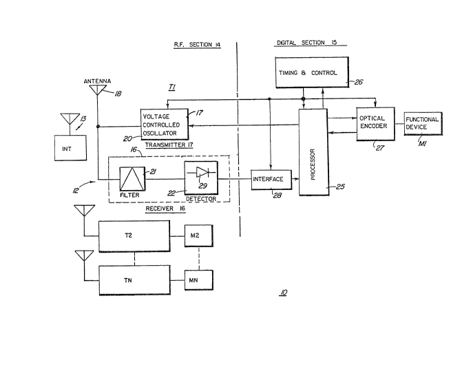
FIG. 1 is a block diagram of a data transmission
system including a data integrity checking arrangement
provided by the present invention;
FIG. 2 is a schematic circuit diagram of the digital
section of a transponder of the system of FIG. 1;
FIG. 3 is a flow chart illustrating the operation
of the receiver during processing of data;
FIG. 4 is a flow chart illustrating the operation
of the receiver during a subroutine for processing incoming
data;
FIG. 5 is a flow chart illustrating the operation
of the receiver during checking and verifying incoming data
bits and data words;
FIG. 6 is a block diagram of a signal processor
circuit of a second embodiment for a transponder for the data
transmi~sion system; and
` ~2682~'7
FIG. 7 is a timing diagram for the signal processor
circuit ~hvwn in FIG. 6.
DESCRIPTION OF PREFERRED EMBODIMENT
Referring to FIG. 1, the data transmission system
of the present invention is described with reference to an
application for providing automatic readout of data which
is provided by a plurality of clata sources M1, M2, ... MN,
which may be data indicating devices such as registers of
utility meters, business machines7 etc. A plurality of
transponders 12 are provided, each associated with one of
the data sources, such as transponder T1 for data source M1.
A radio link is established between the transponders
12 and an interrogate source 13 which may be fixed or located
within a mobile vehicle. The interrogate source 13 transmits
an interrogate signal to the transponders, and each
transponder responds to its unique interrogate signal to
generate a reply signal representing, for example, the current
reading of the register of its associated functional device
and transmit the reply signal back to the interrogate source
13. The interrogate signal is coded to represent a unique
serial number or address for each of the transponders to
permit selective readout of the information registered by
the associated functional device. An example of an
interrogate source suitable for use in such system is
disclosed in above-referenced U.S. Patent No. 3,705,385, and
accordingly, only the transponder will be described herein.
Each transponder, such as transponder T1, comprises
an RF section 14 and a digital section 150 The RF section
14 has a receiver 16 and a transmitter 17 both which are
diplexed to an antenna 18. The transmitter 17 includes a
~ ~ Z~I~Z2~
voltage controlled oscillator 20. The receiver 16 includes
a bandpass filter 21 and a detector 22. The digital section
15 includes a proce~sor 257 a timing and control circuit 26,
an encoder 27, and receiver interface circuit 28.
In the transponder receiver 16, the bandpass filter
21 has its input connected to the antenna 18 and it~ output
connected to the detector 22 which may comprise a crystal
video diode 29, such as the type IN82G. The detector 22 i~
followed by the receiver interface circuit 28.
The bandpass filter 21 defines the response
frequency band for the receiver 16 which is centered at 451
MHz. The voltage controlled oscillator 20 of the transmitter
has a center frequency of 414 MHz and this signal is spread
spectrum modulated with a binary encoded FSK signal
representative of the data to be transmitted to the
interrogate source 13. An example of use of spread spectrum
modulation in a wireless data transmission system is disclosed
in the U.S. Patent 3,967,202 of James E. Batz.
Each transponder is assigned a seven digit serial
number or address which allows it to be uniquely addressed
by the interrogate source 13. The interrogate signal consists
of an eight bit sync word, a four bit command word, indicating
what information is requested, and a twenty-eight bit serial
number or word, representing a seven digit serial number for
the transponder selected for readout. The interrogate source
generates an interrogate signal by amplitude modulating the
451 MHz transmitter carrier with a digital code signal. The
digital information is encoded by varying the duration o~
50% duty cycle pulses o~ a single cycle of 2.77kHz, or
1.786kHz representing a logic 0 or a logic 1, respectively.
~26B2~'~
Thus, a binary 1 is represented as a cycle of 560 microsecond~
duration while a binary 0 is a cycle of 360 microseconds
duration.
The receiver 16 detects the incoming amplitude
modulated signal, recovering the low frequency di~ital
information and the interface circuit 28 generates short
duration pulses which serve as interrupts to the processor
25. The period between the pulses corresponds to the period
of the incoming data.
The processor 25 processes the incoming digital
information under software control, providing bit and word
verification operations, reformulates the sync word, command
word and serial number word of the interrogate signal, and
generates control commands for enabling the transmitter 17
to transmit data when receipt of a valid address i9 verified.
The processor 25 also monitors the encoder 27
associated with the register of the functional device M1 to
receive and store data indicative of the reading of the
register prior to transmission of the data to the interrogate
source 13. The timing and control 26 provides a time base
for the transponder circuits and defines a low power-idle
mode in which the processor 25 is activated for approximately
1% of the time. The timing and control 26 controls reset
operations for the processor 25~
More specifically, the timing and control 26
activat~s the system clock, resetting the processor 25 and
enabling it to respond to the interrupts. The processor 25
times the interval between successive interrupts to determine
if the incoming bit is a logic 1, a logic O or an invalid
bit. Any detection of an invalid bit results in the
1268~:'7
termination of any further processing Or the current
interrogate cycle. After eight valid bits have been received,
the "received" sync word is checked with a stored sync word
and if comparison i3 indicated, the interrogate cycle
continues. When the twenty-eight bit code for the serial
number has been received, the serial number word is checked
with a stored w~rd.
When a valid interro~Jate signal is received and
the received serial number code corresponds to that assigned
to the transponder, the processor 25 controls the transmltter
17 in transmitting the data as requested, as indicated by
the command word, either the reading of the register
associated with the data source M1, or the serial number of
the transponder.
The transmitter 17 replies with a 414 MHz carrier
spread spectrum modulated with a binary encoded FSK signal.
Modulation frequencies of 45.45 kHz and 50.00 kHz are used
to represent binary values of "0" and "1", respectively~ with
each bit having a 360 microsecond duration.
The timing and control 26 provides a power
conserving feature. ~ormally, the timing and control 26
maintains the transponder circuits in a low power mode by
disabling the processor clock. Approximately once every
second, the timing and control 26 allows the processor 25
to operate. During this time, the processor 25 updates the
reading, then enables the receiver 16 to "listerl' for an
interrogate signal. When no interrogate signal is present,
the timing and control 26 disables the clock, typically within
30 millisecond~. The transponder circuits ar~ placed in a
low power mode for another second, and the cycle repeats.
`~ 126~2~
If an interrogate signal is detected while the processor 25
is running, the processor 25 overrides the timing and control
26. The processor Z5 is programmed to stay active as long
as a valid interrogate signal is being received. The low
power mode as ~ell as low power consumption characteristics
of the processor 25 and other transponder circuit devices
enables the transponder circuits to be battery powered.
In the normal mode of operation, the transponder
circuits become active approximately once each second, update
the reading if necessary. If an interrogate signal is not
being received, the unit returns to its low power mode for
another second. An interrogation signal is recognized by
the 360/560 microsecond period of the received data and the
periodic reception of a sync word. ~hen an interrogation
; signal is received, the processor 25 checks to see if the
serial number in the interrogation signal can be matched to
its own. If they match, the command word is checked ts see
what in~ormation is requested, i.e. the serial number or the
reading. The transponder then responds by transmitting the
appropriate information.
Transponder Digital Circuits
Considering the digital section 15 of the
transponder in more detail, w~th reference to FIG. 2, the
processor 25 is commercially available as the RCA type signal
CDP1804A single chip microcomputer, an 8-bit CMOS processor
; which provides 2 kilobytes o~ ROM permanent program storage,
64 bytes of RAM and an internal programmable timer/counter
and internal 16 X 16 bit register array used for program
counters, data counters and data registers. The microcomputer
has three input/output control lines N0-N2, four software
~Z~ Z~'7
testable input event flag line3 EF1-EF4, and a single bit
output line Q which can be set and reset under software
control or by the timer-counter~ One external interrupt line
INT is also provided~ The microcomputer also has eight data
inputs of which BUS 0 and BUS 2 are used, eY.ternal clock
timing inputs XTAL and CLOCK, and two control input3 WAIT
and CLEAR.
The optical encoder Z7 include~ a light source 27a
! and a detecting circuit 27b and is used to detect the position
of an interruptor disc ~not shown) attached to an indexing
mechanism of the data source register. The dise is configured
to shade the detecting circuit 27b from light ~rom the light
source 27a as the di~c turns. The detecting circuit 27b
provi de~ outputs over a pair of output lines 27c and 27d
indicative of an unambiguous indication of the completion
of a revolution of the disc. The processor 25 monitors these
output lires 27c and 27d and reglsters a cummulative count
corresponding to the number of revolutions of the diso, thus
pro~iding information indicative o~ the reading of the data
source register. An example of an encoder suitable ~or this
application is disclosed in U.S. Patent ~o. 4,634,859 issued
January 6, 1987 to Dennis J. Martell and which is assigned to the
assignee of this application.
The timing and control 26 includes a crystal clock
oscillator 31, a timer circuit 32~ a timeout delay network
33, a timeout override circuit 34, and a transmitterJencoder
enable clrcuit 35.
The crystal clock oscillator 31 includes a 2MHz
crystal 41, a resistor 42 and capacltor 43 connected in
parallel with the crystal 41. The 2~Hz crystal 41 is
1 0
Z2'7
connected to the on-chip oscillator terminals XTAL and CLOCK
to provide a clock source which sets the machine cycle at
4 microseconds. The clock signal is also fed to one of the
event flag lines EF1 to provide a source for the counterttimer
circuit. The other event flag lines EF2 to EF4 are connected
to a programmer network 46 to set their logic levels ko define
different operating modes for the processor 25. In the
present embodiment, the processor 25 is set to operate under
software control to transmit either its data or its serial
number in accordance with the command word information
transmitted in the interrogate signal.
The timer circuit 32 includes a multivibrator 51
configured in a monostable mode with a pulse period of
approximately one second which is determined by an external
timing network, formed by capacitor 52 and resistor 53, which
is connected to the timing inputs R, C, and RC of the
multivibrator 51. When the multivibrator 51 is triggered
by a pulse applied to its trigger input T, the true output
Q of the multivibrator 51 goes high. ~Ihen the multivibrator
51 times out7 its false output Q1 goes high.
The true output Q of the multivibrator 51 i5
connected through diode 68' to input WAIT of the processor
25 and through diode 47 and resistor 42 to the CLOCK input
of the processor. The true output Q of multivibrator 51 is
also connected to an inhibit input of amplifier circuit 103.
A reset network 54 formed by resistor 55, capacitor
57 and diode 58 is connected between the true output Q of
the multivibrator 51 and its reset input R. The reset network
54 allows the level at R to reach the logic 1 condition to
; 30 reset the multivibrator 51 if the pulse on output Q i-q
1 ~
lZG8Z;27
appreciably longer than one second, indicating a latchup
conditionO The false output Q of the multivibrator 51 i5
connected to the power input of the encoder detector circuit
27~. .
The timeout delay network 33 includes tandem
connected NAND gates 61 and 62 and a timing network formed
by resistor 64 and capacitor 65. The timeout override circuit
34 includes an NPN transistor 66, havin~ an input network
67 including a capacitor 68 and a diode 69 which are connected
between ths output of the crystal oscillator 31 and the base
of transistor 66, and a capacitor 70, which is connected
between emitter and base of transistor 66. A diode 71 is
connected between the emitter of transistor 66 and the
junction of capacitor 68 and diode 69.
The timeout override circuit 34 further includes
an output network 74 including capacitor 75 and resistor 76
which are connected in parallel between the collector of
transistor 66 and ground. ~ resistor 77 is connected between
the base of transistor 66 and ~round. The collector of
transistor 66 is connected to the input WAIT of the
microcomputer and through a diode 78 to the junction of
resistor S4 and capacitor 65 at point 80 to which is connected
one input 62a of NAND gate 62 which has its other input 62b
connected to the output of NAND gate 61. NAND gate 61 has
its input~ connected to respective outputs N1 and N2 of the
processor 25. Processor output N2 is also connected through
diode 81 to point 80. In addition, the true output Q Or
multivibrator 51 is connected through diode 82 to point 80.
G~227
The transmitter/encoder enabling circuits 35 include
a latch circuit 91 ha~ing a set input connected to the output
NO of the processor 25, and a reset input connected to the
output of a reset gate 929 embodied as a two-input NOR gate,
wh;ch has its inputs 92a and 92b connected to processor output
; N1 and multivibrator output Q, respectively. A data drive
circuit 93 has its input connected to the processor data
; output Q and its output connec:ted to the drive input of the
voltage controlled oscillato~ 20 (FIG. 1).
Control of the operation and readout of the encoder
27 is ef~ected through transmission gates 95, 96 and 97.
Transmission gate 95 has its input connected to the data
output Q of the. processor, its output connected to the power
supply input of light source 27a of the encoder 27, and its
enabling input connected to the false output of latch circuit
91. Transmission gates 96 and 97 are connected between
respective encoder output lines 27c and 27d and respective
data inputs BUS 0 and BUS 2 of processor 25. The enabling
inputs for transmission gates 96 and 97 are commonly connected
to processor output N1. In addition, the power input to the
detecting circuit 27b is connected to output Q of the
multivibrator 51.
Referring now to the receiver interface circuit
28, this circuit includes a high gain linear amplifier stage
101, an edge detecting circuit 102, and a slicing circuit
; 103 which is interposed between the amplifier stage 101 and
the edge detecting circuit 102. The elements of the interface
circuit 28 are well-known in the art and accordingly are shown
. 13
- ~ (
~LZi8;2; :7
in block diagram form in FIG. 2. The amplifier stage 101
amplifies the AC signal output of the detector 22 which is
the 2.77 kHz or 1.786kHz digital code signal.
The slicing circuit 103 limits this signal,
providing a square wave signal 560 microseconds in duration
for each logic 1 bit and 360 microseconds for each logic 0
bit of the interrogate code. The slicing circuit 103 has
an input connected to the true output Q of the multivibrator
so that ~he slicing circuit 103 and the ed~e detecting circuit
102 are inhibited when the receiver circuits are in the
low-power mode.
The edge detecting circuit 102 responds to the
output of the slicing circuit 103 to provide interrupt pulses
to the processor 25 by converting the rising edges of pulses
in the data stream into short pulses of 30 to 40 ~icroseconds
duration. The processor 25 measures the period between these
pulses to determine the length of the incoming data bits.
Operation of the Transponder Digital Circuits
As an aid in understanding, it will be beneficial
~o describe the operation of the hardware circuits of the
receiver before describing the system operation and the
software which controls the processor 25.
Referring to FIG. 2, the timing and control 26
normally maintains the transponder circuits in the low power
mode but activates them for about 30 milliseconds once every
~ second. As indicated, the multivibrator 51 is configured
; in a monostable mode, with a pulqe period Or approximately
one second set by capacitor 52 and resistor 53. When the
multivibrator 51 is triggereds its true output Q is high and
; 30 its false output Q is low. This keeps the transponder
14
-
lZ6132;~'7
circuits in the low power mode. With output Q low, thi~ turn~
off the power to the detecting circuit 27b. With the Q output
high, the crystal clock oscillator 31 is kept from running
by diode 47 which pulls the processor CLOCK input high.
Stopping the processor clock reduces its power consumptivn
significantly. The WAIT line of the processor 25 i8 also
held hi gh thru diode 68' by the high le~el on the
multivibrator true output. With the processor WAIT line high
and its CLEAR line low, the processor 25 is held in a reset
state. The high level on the rnultivibrator Q output also
keeps slicing circuit ~03 and the edge detecting circuit 102
in a inactive state.
~ 7hen the multivibrator 51 times out, its Q output
goes low and its Q output goes high. This enables the slicing
circuit 103 and the edge detecting circuit 102 of the receiver
circuitry and supplies power to the detecting circuit 27b.
The high level clamps on the CLOCK and WAIT inputs of the
processor 25 through respective diodes 68' and 47 are
released. This allows the crystal clock oscillator circuit
31 to begin to run. Also released is the high level clamp
through diode 82 to input 62a of gate 62. Transistor 66
continues to hold the WAIT line of the processor 25 high until
the crystal 41 has begun to oscillate and the output of the
crystal oscillator circuit 31 has begun to stabilize. The
oscillator signal turns off transistor 66 by pulling its base
high through capacitor 68, and diode 69. When the WAIT output
goes low, the processor 25 is placed in the run mode~
When input 62a of gate 62 is unclamped due to
timeout of multivibrator 51, it initially remains high due
to the high signal supplied by transistor 66 through diode
6~32Z'7
78 when the transistor 66 is conducting. When tran~istor
66 turns off and the processor 25 begins to run, input 62a
of gate 62 is held high by the charged state of capacitor
65. Capacitor 65 beginq to discharge; and if undisturbed,
the voltage on the capacitor 65 reaches the switching
threshold of gate 62 in about 10 milliseconds~ Note that
the other input of gate 62 is held high by gate 61. When
the threshold is reached, gate 62 generates a trigger pulse
that starts the multivibrator 51, placing the transponder
; lO circuit back into a low power mode.
The processor 25 can clelay the entrance into the
low power mode by generating pulses on its output N2. These
pulses c~arge capacitor 65, increasing the voltage level on
the timing capacitor 65. By repeatedly pulsing this output,
the processor 25 can override timing and control 26 to keep
the transponder circuits active as long as required to
complete the processing of data during an interrogate cycle.
The processor 25 also has the abili~ty to immediately place
the transponder circuits in the low power mode by
simultaneously pulsing its N2 and N1 lines. This generates
the trigger pulse thru gate 62 required to start the
multivibrator 51. The multivibrator 51 has a fail-safe
feature using the timing network comprised of resistor 55
and capacitor 57. If the output pulse of the multivibrator
51 significantly exceeds its one second duration, the
multivibrator 51 is reset by a high level provided-at its
RES~T input by the timing network.
To read the encoder 27, the processor 25 sets its
output Q high. Transmission gate 95 is normally maintained
conducting when the transponder is not transmitting so that
~lZ682~'~
the signal on output Q i~ extended through transmission gate
95 to enable the light source 27a.
To read the ~tatus of the detector 27b, the
processor 25 pulses its output N1 which enables transmission
gates 96 and 97, connecting the outputs of the encoder at
lines 27c and 27d to inputs BUS 0 and BUS 2 of the processor
25. The processor 25 reads these inputs, processes the
information provided and when appropriate, updates the count
registe~ which stores th0 reading provided by the associated
functional device.
To transmit a reply, the processor 25 turns on the
transmitter 17 by setting latch circuit 91 and supplies the
modulation signal to the data drive circuit 93 via output
Q. The setting of latch circuit 91 causes application of
power to the transmitter oscillator 200
Modulation representing the information to be
transmitted i8 generated by the processor 25 and appears at
its Q output line in the form of a 45kHz/50kHz FSK square
wave signal. When the transmitter 17 is enabled, transmission
gate 95 i3 disabled by latch circuit 91 and keeps the
modulation on the processor's Q line from turning on the
; encoder light source 27a. In order to turn off the
transmitter, the processor 25 pulses its N1 line, which resets
latch circuit 91 via gate 92.
Trans onder Software Control
P - .
The processor 25 operates under program control
to receive and proce~s the incoming interrogate signal and
verify the incoming interrogation code as it is received,
to read the status of the encoder outputs and accumulate data
representative of the reading~ and to verify receipt Or the
~6~32~:>Y
address of the transponder and to control the transmitter
in sending the stored data back to the interrogate source
13.
The program consists of a main routine the rlow
chart for which is shown in FIG~ 3, an interrupt routine the
flow chart for which is shown in FIG. 4, and a data bit
verification routine the program f`low chart for which is shown
in FIG. 5. A program listing is provided in Appendix I.
The main routine controls the initialization of
the processor circuits, setting up the processor 25 to receive
data. The main routine also controls forming of the sync
word, the command word, and the serial number, as the bits
are received, matching of the serial number and enabling the
transmitter when a match is detected. The interrupt routine
handles receipt of the input bits from the edge detecting
circuit and the storing of each valid bit as it is received.
The verification routine verifies valid bits and valid data
words and terminates interrogate operation whenever a selected
member of invalid bits or words is detected. In the exemplary
embodiment, the interrogate cycle is terminated whenever five
bad bits are detected or if 128 valid bits are detected before
a valid sync word has been recei~ed.
More speci~ically, referring to FIG. 3, the main
receiver routine 160 provides at block 161 for activation
. of the processor 25 in response to the timing and control
26. The processor performs housekeeping activities block
162, such as reading external status lines, and at block 163,
sets up to recei~e data. The receiver main program also forms
the multi-bit interrogate word, blocks 164-166, including
the eight bit sync word, the four bit command and the
18
.-- l
~L2~3Z2'7
twenty-eight bit serial number from the incoming data, and
performs the internal address match at block 167, activating
the system at block 168, to respond when the proper serial
number is verified and to activate the transmitter 17. During
processing of the sync word, i~ a bad bit is detected or if
less than eight bits have been received, the system enter~
the bad bit routine at block 169, shown in detail in FIG. 5
and deactivates the system at block 170 if fiv~ bad bits or
128 good bits have been received before a sync word has been
received. Then in the event an error is detected during
processing of the command word at block 165 or the serial
number at block 166, the system returns and the routine is
reinitiated. Likewise, if a valid serial number match is
not detected, the system returns and reinitiates the routine.
The power down operation effected at block 170 results in
the processor 25 halting operation and awa;ting timeout by
timing and control 26.
Referring now to FIG. 49 the interrupt routine 171
is entered each time data is provided over the interrupt
line. Once the main program has completed housekeeping
operations and is set up to receive data, interrupts are
enabled at block 172 and the system reverts to an idle mode
at block 173 awaiting an interrupt. When an interrupt is
detected, the system at block 17~ disables further interrupts
temporarily while processing operations are e~fected. At
block 175, the previouq count, representative of the frequency
of the incoming signal if t~is is the second interrupt, is
stored and the interval timer is started at block 176 to time
the duration between the present interrupt and the next
interrupt. At block 177, the bit value is determined by
1 9
126~
checking the stored count which represents the time between
successive interrupt~, to determine if the bit received i~
a logic 0, a logic 1 or a bad bit. This bit value information
is determined by the verification routine at block 186
(FIG. 5)~
Referring to FIG. 5, the verification routine ia
illustrated as flow chart 180. This routine is entered from
the main receiver program and involves initiating the bad
bit counter at block 182 and the bad word counter at block
184. Block 185 is the interrupt routine illustrated in FIG. 4
which receives and processes the incoming information. In
blocks 186-189, the verification routine determines if a good
bit has been received, and if the expected sync word has been
received, and if so~ the bad bit counter is set to "O". The
main system routine is entered at block 189 (blocks 165-1~7
in FIG. 3), where the routine is completed.
Blocks 190-193 detect receipt of a bad bit,
including checking to see how many bad bits have been
received, decrementing the bad bit counter and initiating
a power do~n operation when the bad bit counter is decremented
to zero. Blocks 194-196 provide a corresponding operation
for checking the number of bits which have been received and
effecting power down when the number of good bits exceeds
the count of 128 before a sync word is detected.
System Operation
.
Referring to FIG. 1, to read out the information
representing the meter M1 D the interrogate source generate3
an interrogate signal by amplitude modulating the 451 MH~-
transmitter carr;er with a digital code signal to represent
the sync word~ the command word and the serial number for
,.,, ! ~
1~6EiZZ'7
transponder T1. The digital information is encoded by vary~ng
the duration of 50% duty,cycle pulses of a single cycle of
2.77kHz, or 1.786kHz representing a logic 0 oP a logic 1,
respectively. Thus, a binary 1 is represented as a cyclç
of 560 microseconds duration while a binary O is a cycle of
360 microseconds duration.
The receiver 16 detects the incoming amplitude
modulated signal, recovering the low fre~uency digital
information and the interface circuit 28 generate~ short
duration pulses which serve as interrupts to the processor
25. The period between the pulses corresponds to the period
of the incoming data. Data bits with a period from 260
microseconds to ~60 microseconds are interpreted as logic
0 bits while data bits with lengths from 460 to 660
microseconds are interpreted as logic bits. Detections
outside of these periods are considered a bad bit.
The processor 25 processes the incoming digital
information under software control, providing bit and word
verification operations, reformulates the sync word, command
word and serial number word of the interrogate signal, and
generates control commands for enabling the transmitter 17
to transmit data when rec,eipt Or a valid address is verified.
Referring to FIGS. 3-5, the transponder processor
25 begins executing the program stored in the ROM each time
it is activated (block 161) by the timing and control 26.
The fir~t operation i5 to disable interrupts. Since the
external interrupt line of the processor is used for resolving
incoming data from the receiver, the interrupt signal from
the receiver is disabled until the processor has set up the
interrupt routine and i~ ready to receive. Next, the software
' 21
~6~Z2'~
performs several initialization steps, setting up pointer~
and flags to default values.
A second part of initialization is to check the
outputs of the optical encoder 27 to determine the position
of the interrupter disc. The processor ackivates the light
source 27a and reads the state of the detector 27b on lines
27c and 27d. If both lines are low, a flag called MFLAG is
reset. If they are both active and MFLAG is in a reset state,
the reading is incremented, and MFLAG is set. The
intermediate conditions of one line active and one inactive
is ignored. MFLAG is used as a toggle to indicate the partial
revolution of the interrupter disk.
In the meter reading portion of the program, a
counter called LOOPCOUNT is set to 200 following the encoder
reading and meter update. During the data receiving loop
portions of the program, this counter is decremented each
time a bad bit or an invalid condition (e.g., illegal command,
unmatched serial number, etc.) is detected. If the LOOPCOUNT
counter reaches zero, the software returns to the beginning
of the program. This insures that the transponder can
continue to update the meter reading even though it may be
under continuous interrogation~ Under the absolute wor~t
case conditions the meter encoder will be read every 40
seconds. A more typical value under normal interrogation
conditions is ~ seconds.
After the reading is checked, the program enters
the data receiving loop routine, blocks 163-169, the central
portion o~ the transponder software, where the incoming data
is resolved (~ia the interrupt and verification routines).
The data receiving loop software also determines i~ the
~L26~ZZ7
transponder circuits should stay active, or return to the
low power mode~ After initialization, the interrupts are
enabled, block 172 (FIG. 4) and the processor enters the idle
mode block 173 awaiting an interrupt, corresponding to the
first detected bit of the interrogate code transmitted by
the interrogate source 13.
The interrupts provided at the output of interface
circuit 28 (FIG. 1) are fed to the interrupt input of tne
processor. The interrupt routine (FIG. 4) measures the period
between interrupts, and thereby measures the receiver data
bit lengths. It utilizes the processor internal timer circuit
to do this. The internal timer is configured to count the
2 MHz processor clock when activated.
Referring to FIG. 4, when an interrupt is detected,
the interrupt routine 171 is entered and at block 174 further
interrupts are disabled. The count registered by the timer
, counter is stored and the counter is restarted. Then the
verification operations are carried out. The timer counter
count value is checked for an overflow, i.e. indicative of
a time period greater than 660 microseconds. An overflow
indicates the previous bit time was too long to be a good
bit (longer than 660 microseconds). On a counter overflow,
the bad bit routine 180 (FIG. 5) is entered. If a counter
overflow has not occured, the interrupt routine sets a new
interrupt pointer to the bad bit routine, and interrupts are
then enabled and the internal timer is reset and restarted
at block 176. Now i~ an interrupt occurs, it indicates a
period too short (less than 260 microseconds) to be a good
bit, and the bad bit routine is again entered.
~Z68Z;2~
The interrupt routine at block 177 then calculates
the value of the previous bit based on the timer count (block
175) which has been stored, and at block 178 return~ to the
main program at blocks 164-166 (FIG. 3). The main program
stores the value of the b;t returned by the interrupt routine,
and changes data pointers and counters if necessary. Finally,
the main program change~ the interrupt pointer back to the
standard interrupt routine at the time corresponding to the
start of a valid "0" bit, approximately 260 microseconds after
the previous interrupt. The main program then reenters an
idle state (blocks 172-173), waiting for the next interrupt.
An external interrupt from a good bit must ocour or élse the
timer counter will overflow and generate an internal
interrupt. In either case, the interrupt routine is ertered
again, and the process repeats to receive the remaining bits
of the sync word, the four bit command word and the 28 bit
serial number.
Since the interrupt routine expects the timer to
be running when an interrupt occurs, it is necessary to catch
the first bit and start the timer at the beginning of
receiving a bit stream. When the data receiving loop is first
entered, several pointers, counters, and flags are
initialized. Then a short routine is entered that looks for
the next interrupt pulse, although the interrupt routine is
not enabled yet. When it occurs, the interrupt routine timer
count is started, and external interrupts are enabled. Now
the program can jwnp to the interrupt routine on each received
bit pulse, and return to the main program with the bit value.
Each time the interrupt routine is entered and a bit is
determined to be good, the proce~sor isQues a reset pul~e
24
3227
to the circuit timer and decrements the badword counter one
coun$. This counter is set to an initial count of 128 at
the start of an interrogate cycle. If an interrupt does not
occur or if only bad bits are received, the timer eventually
resets the processor and returns the unit to a low power mode,
block 170.
~ hen a bit is too long or too short to be good,
the verification routine (FIG. 5) is entered This routine
resets the interrupt pointer, and at blocks 190-192 keeps
track of bad bits and checks to see if five bad bits have
been received since the last valid sync word. If five bad
bits have been received, at block 193 the processor enables
the timing and control 26 to place the system in the low power
mode. If less than five bad bits have been received, control
is passed back to the beginning of the data receiving loop
routine.
Regarding the manner in which the sync word, the
command word and the serial number word are formulated, once
the first bit edge is caught, the data receiving routine keeps
shifting the subsequent bits returned by the interrupt routine
through a buffer. The buffer is checked each time for the
presence of a series of eight valid bits having the coding
that corresponds to the sync word coding stored in RAM. If
128 good bits are receiYed before a Yalid sync word has been
received (block 187), the program (blocks 194-196) jumps to
an instruction which causes the unit to return to the low
power mode.
Referring to FIG. 3, i~ a valid sync word i5
detected, the program assumes that it has found tbe beginning
of an interrogation transmission. Data pointers are changed,
3ZZ~Y
and the next four bits received are stored in a COMMAND
register (block 165). Again poinkers are changed, and the
following 28 bits are stored in the memory (block 166)~ If
while receiving the command or serial number bits, a bad bit
is detected, the program returns to the beginning o~ the data
receiving loop. Pointers and registers are re-initialized,
and the receiving process starts again.
Once reception of a serial number is complete, the
loop routine continues by checking the received serial number
(block 167). If all seven received serial number digits can
be matched, then the requirements for a response will have
been met, and the software jumps to the transmit portion of
the software.
The transmission routine ~enerates modulating
frequencies by using the internal timer to divide down the
2.0 MHz clock signal appearing at the EF1 pin of the processor
25 to 45.45 kHz and 50.00 kHz. The transmitter 17 is
activated by setting latch circuit 91 The processor Q output
line is then toggled at these frequencies to provide
transmitter modulation via data drive circuit 93 ~FIG. 2)c
To transmit a bit, the software needs to obtain the bit to
be transmitted, load the proper divisor into the internal
timer, direct the output to the processor Q line9 and wait
for one bit time ~360 microseconds). This process is repeated
for each transmitted bit.
When the routine is first entered, the transmitter
17 is turned on and a constant 45.45 kHz modulating frequency
is generated. The software then waits for a short time,
26
lZ~B227
causing slightly more than two complete "1" bits to be
transmitted previou~ to the data transmission. This delay
allows the transmitter circuit to stabilize.
The routine then reads the COMMAND register and
checks to see if a reading or serial number was requested.
Consequentlyg the routine then sets data pointers to either
the permanent serial number memory or the permanent reading
memory. In either case, 28 bits are examined sequentially
and the corresponding modulating frequencies are generated
for 360 microseconds for each bit. Following the transmission
of the 28 bits~ the processor 25 turns the transmitter 17
off.
Second Embodiment
In the foregoing embodiment, a processor operating
under program control verifies the validity of the incoming
interrogate signal by checking the incoming signal on a
bit-by-bit basis and checks the received sync word and the
received identification word portions of the signal with
stored words. It is apparent that these operations can also
be done by discrete circuits. For example, referring to FIGu
6, there is shown a block diagram of a second embodiment of
a signal processor circuit 200 provided in accordance with
the invention wbich employs discrete circuits for providing
the interrogate signal verification operation described
above. The processor circuit 200 includes an interface
circuit 201, an edge detecting circuit 202 and a veri~ication
circuit 203. Operation Or the processor circuit 200 is
synchronized by a timing circuit 204 which provides square
wave signal at a 100 kHz rate.
lZ6B227
The edge detecting circuit 202 includes a four-bit
shif't register 2119 a decoder circuit 212 and a reset circuit
213 including a NAND gate 214 and an inverter 215.
The verification circuit 203 includes a counter
cirouit 221, a decoder circuit 222, a reset circuit 223, and
an output register section 224 including a sync word shift
register 225, an identification code word register 226 and
an error register 227. The verif`ication circuit 203 also
includes a strobe signal generator 228, a data compare circuit
lO 229 and a control circuit 230.
The interface circuit 201 includes a high gain
linear amplifier 201a having its input connected to the output
of detector 22 (FIG. 1). The amplifier 201 amplifies the
AC output of the detector 22 which is the 2.77 kHz or 1.786
kHz digital code signal. The output of amplifier 201a is
applied to a slicing circuit 201b which limits this signal,
providing a square wave signal which is 560 microseconds in
duration for éach logic 1 bit and 360 microseconds for each
logic 0 bit of the interrogate code. The output of the
20 slicing circuit is connected to the data input of the four-bit
shift register 211. The shift register 211 is clocked by
the leading edges of 100 kHz square wave timing signals
provided by timing circuit 204. The decoder circuit 212
responds to outputs of the shift register 211 to provide a
positive going signal output from gate 214 whenever the data
input of the shift register is maintained low for three
successive clock signals after being in a high state,
indicative of detection of the negative going edge
28
.
~68;~2'~
of a data bit in the incoming interrogation ~ignal stream.
The three cycle delay provides a degree o~ immunity from noise
for the processor circuit 200.
Counter circuit 221 is connected for operation as
an inter~val timer and responds to the timing signals provided
by timing circuit 204, to time the duration of each bit of
the incoming signal and indicate whether the detected bit
is a logic 1, a logio 0 or an error bit. The counter 221
is held reset by reset circuit 223 in the absence of an
incoming signal, but is enabled by the positive pulse from
gate 214 to count the timing signals when the negative edge
an incoming signal is detected until the detection of the
next negative going edge of the succeeding data bit. Thc
decoder circuit 222 decodes the outputs of the counter and
provides an output on data line 222a indicating that the input
signal is a logic 1 when the elapsed time is in the order
of 560 microseconds, or a logic 0 when the elapsed time is
in the order of 360 microseconds, or on an error line 222b
when the count stored by counter 221 represents a time period
outside of the range representing logic 1 or logic 0~
Register 227 responds to the error signal and generates an
error reset signal for resetting data shift registers 225
and 226.
The sync word shift register 225 receives and
decodes the first eight bits which correspond to the sync
word portion of the incoming interrogate signal. Shift
register 226 receives and store the twenty-eight bit
identification word portion of the interrogate signal as ~t
is received. Each shift register 225 and 226 has a clock
input connected to the output of the decode circuit 212 to
.
1~6BZ2'7
receive a ~hift pulse generated with the detection o~ each
falling edge of the incoming data signal. Shift registers
225 and 226 have a reset input connected to the output of
the error register 227 to enable reset of the registers 225
and 226 upon detection of an error bit. The shift registers
225 and 226 have associated decoder circuits 225' and 226'
which provide respective outputs indicating receipt of a valid
sync word and the identification code assigned to the
transponder when such data is received in the corresponding
register.
The data compare circuit 229 has its input connected
to the outputs of decoder circuit 222 enabling valid bit
signals to be gated by strobe signals generated by strobe
signal generating circuit 228 to the control circuit 230.
Control circuit 230 sequences the operation of the processor
oircuit 200, including routing of incoming data bits first
to the sync register 225 until a valid sync word is detected7
and then to the identification code word register 226.
OPERATION
; 20 Referring to FIG. 6 and to FIG. 7, which is a timing
diagram for the processor circuit 200 shown in FIG. 6, the
timing circuit 204 provides timing signals at a 100 kHz rate
for synchronizing the operation of the processor circuit 200.
The edge detecting circuit 202 enables the counter 221 to
count the timing signals for the duration of each bit of the
incoming interrogate signal9 that is, until the counter is
reset by the reset circuit 213.
The timing signals, FIG. 7, line Ay generated by
the timing circuit 204 are also supplied to the clock input
of the shift register 211. ln response to trailing edge of
\
~L2~ Z'~
each signal of the incoming bit stream, the ~hift register
211 responds to the leading edges of the timing signal, FIG.
7, line B, to shift the signal level (FIG. 7, line C)
appearing at its data input through the four stage shift
register. The outputs are decoded by circuit 212 so that
after three timing signals, FIG. 7, line B, following the
falling edge of the signal at the shift register data input
(line C) the output of the decoder circuit 212 goes high,
FIG. 7, line D. This signal is applied as a counter reset
signal through gate 2149 when strobed by a clock signal (See
FIG. 7, line E) through inverter 215, to enable reset circuit
223 to reset the counter circuit 221.
The counter circuit 221 then counts the timing
signals at the 100 kHz rate provided by timing circuit 204
until it is reset by the next counter reset signal generated
by shift register 2119 decoder circuit 212 and gate 214.
At such time~ the count of the counter circuit 221 corresponds
to the period of the incoming data bit, a logic 0 being
represented by a count of 24 to 47 corresponding to a period
; 20 of 240-Y70 microseconds ~etween negative transitions and a
logic 1 being represented by a count of 48 to 63 corresponding
to a period of 480-630 microseconds between negative
transitions~ As each negative transition occurs, the counter
condition is observed to determine the binary Yalue of the
previous data bit received (See FIG. 7~ line F~.before
resetting the counter for a new daSa bit time measurement.
If the data period is from 40 microsecond~ to 470
microseconds, decoder circuit 222 provides a logic O level
on data line 222a. If the data period is from 480
microsecond~ to 630 microseconds, decoder circuit 222 proYide3
31
12~6B2Z'7
a logic 1 level on data line 222a. When the data period is
less than 240 microseconds or longer than 630 microseconds,
the decoder circuit 222 provides an output on error line 222b
which causes error register circuit 227 to reset the shift
; registers 225 and 226.
With reference to FIG. 7, line D, the output of
decoder 212 is generated with the leading edge Or timing
signals whereas the counter reset, signal E, is generated
in response to enabling of gate 214 which is effected by the
trailing edge of the timing signals. During this delay time,
the output of the counter decoder circuit 212 is applied to
the sync word shift register 225, being clocked into the shift
register 225 by the rising edge of the decodersignal, FIG. 7,
line D. In addition, the output of the decoder circuit 222
is applied to data compare circuit 229 which is strobed by
a strobe signal FIG. 7, line F generated by strobe signal
generating circuit 228, which generates a positive going pulse
in response to the detection of each bit. This signal is
applied to the control circuit 230 which controls steering
i 20 of the bits between the sync word shift register 225 and the
: identification code word register 226.
After a valid eight bit sync word has been detected,
as indicated by an input to the data compare circuit 229
provided by the decoder circuit 225' associated with the sync
word register 225, the control circuit 230 causes the next
four bits, which are the operation command~ to be stored in
a suitable register (not shown) and then directs the remaining
twenty-eight bits of the interrogate signal to the input of
the identification code shi~t register 226.
~'~6BZZ~
After a twenty-eight bit identification word has
been received in the identification code shift regisker 226,
the decoder 226', associated with the identification code
shift register 226, generates a signal TRAIISMIT ENABLE if,
and only if~ the identification code received in shift
register 226 corresponds to that assigned to the transponder.
In the event a bad bit is received, an indication
is provided over error line 222b at the output of decoder
222 which is stored in error register 227. This causes the
lO register 227 to generate an error reset signal which resets
the shift registers 225 and 226 to terminate the current
interrogate cycle. In addition, in the event of an overflow
for counter 221, reset circuit 223 is enabled to reset the
counter1 also resulting in an error indication.
The signal TRANSMIT ENABLE generated by shift
register 226 as the result of the verification of the incoming
interrogation signal is used to cause the transmitter to be
activated ar~d to initia'ce the readout OI the information
provided by the transponder registers. Arrangements for
20 effecting these operations are known in the art and have been
described in detail in U.S. Patent 4,040,0469 3,967,202 and
- 3,705,385, for example.
While particular embodiments of the present
invention have been shown and described, it is apparent that
changes and modifications may be made without departing from
the invention in its broader aspects. Therefore, the aim
in the appended claims is to cover all such changes and
modifications as fall within the true spirit and scope of
the invention. The matter set forth in the foregoing
30 descr~ption and accompanying drawings ic~ offered by way of
2'7
illustration only and not as a limitation. The actual scope
of the invention is intended to be defined in the following
claims when viewed in their proper perspective based on the
prior art~
34
~'~6~Z2'7
~ , ~
Q
C r~ r~
4 ~ C
C O Ul ul LL~ ~1
C t)
~nUl 3 ~ ! G ~0
LLI '' ~ X X ~ ~ ~ $ ~C
r~ O O
3 al +~ r~! r~J t~ a tl- ~ 0 0~
Ci'~ 3 C I I 4 ~ 11 IL~ > ~h o o o o o o
O ~ C X l~ O
n o o~ ~ ~ ~x a,
z3 ~ ' G ~ ~ ~ K
-p ~ o o a~ lG P ; 4
Z ~ Ul ~ ~ +~ r~ r r~
X o
H rl ~ ~r l'J N C Ci
Cl ~ o o O `
Z
~ r tl_ O li~ C . _
P' ~ 'Q fO O 11~ ~ ~
Pi ~ e ~
o ~ ~ ~ ~ oI I i I
~ -- 3 0 ~J G C ~ rlI I I I
X X C iL ~
II , ~?: i Z~ I
II I ~ . I ~ I
II O , ' I ~ I
~i Ii N ~' I G I
+ r.] I
H I i ~
o I ~ I IL Z ~4 1 i,l I
~ ~ SrS~ ~ ~ ~ S~_ I I
I Z I t~ O i ~ X --' s~ Z ~ Z ~ 10 1 i i I
:C,--. A I I ~ ; ~ Ci 1~ I 1~ I C; O ~ t,3 1-- X ~ X S' o i~ ',-- i~
o co m ~ n o C~i o ~
N ~0 0 11~ r`J ~ O O O I I I i~ I
~'' I 1- I ~ I
Ci ~ ~ ~ ~ ~ ~ 1 G ~ ~ i I ~ :t 3~ 5-1 H '~
W hi iL1 s~ iLI hi i~ ~ I I S~~ ~1 ~ J :~ 1-- ~: ~ I Z I I I
~ ci J; i i ~ In L ~ i , 3
':C 3 ~i o ~ --O
~1 X X ~ ~'~' C; C ~ '!~ Z ' _I ' ~ ~ - ~ . .. . ...
o Sl-- ~ ~ ~; Sr Z ~ ~ _S ~ ~ ~ - o ~ ~ o ~
_ . _
`-- . . 3 5
O ~ ~ 0. ~
~2~l32~
.p ~ .
o
~ Ql, ~ 4 t_ ~-1 L L ~_
r ~-1 ~ O ~
. ~' ~ o '` Ql ~ ~ ~ ro 4 41 ~ ~^
O G ~ r~ O I ru ~ , o
~U ~ ~ ~ C ~ P.Ci ~ h
3 ~ ~ Ul o~ ~ ~ ~ I,h o ~ (O e
G ~ ~ P O tJ t ~ ~ o ~P
n tJ ~ 1 C ~ . 41 Qln: .C 3 (O
C ~n r ~J *~
f Q! 111 C IJI tll ,p V~ ro .
~n ~ O O 10
O ~ 1 G ~ ~ H 10
~ ~ G t~ G ~o
4 J G rv ~o ~ O C ro ,~ ~p ~
~; G ,C ~ 4: CJ al o ~ "- un n, 3~ t_
o
1~ .C 'r7 ~ J. ' O a~
J iL P .C ~ ~ .C aJ 'Q ~1 , 7 ~J ~ C ~I a. P ~1 U` 7 ~
~ ~ P Iti C ~ .C ~ a, ~ ;P C 4 ,~ ~i
C 'Q Q ~ q- O r- O Ql P -Pt- _.C ' ~ P O aJ q~'
f_ n) r ~ o ot~ -I 3 C~-1.ti ~ 6 t'~ 5-
--~ tL' 1~ tU ;r, ~; r.C O X
~ .. ~ . ,o .. ~ , o . ~ ~ . . . .. . . -- . ~ . . . . . .. . , . o . . , ~, .. .
- '
' ' .
': '
- : :
~ ~ ;~ IL 7~ 1~7 ~1;
`' 1' 0 0 0 ' ~ O _~ O- 7Y ~ O O
~; O O O ~ IL~ IL t~ IL t~ i.L ~!3 ~ ~ ~ o
-- o o ~ o o ~ ~ ~ n o o ~ ~o
C o o 111 o :C ~ J ~ ~ o ~ ;C o C~ _, V
O Z: O ~ I 1~ I O LL I IL I ~ C ~ I O O ~
1`~ O O I~l O l`~ ~ O ~ ~ ~ 0 ~ X O t l O L~ O O X --~ X X X t_)
-- C~ Ci ~ ~ h. C~X ~ ~ ~ O ~ ~ O ~ ~ X ~: X IL X i~. ~ ~1 X i-- ~ C X l_ Y O
JJ ~' G O Z~ Z y ~ 1 Y J !~' ~ ~ J Z ~ Z ~ _ ~ z ~ _ z ~ z
J h tJ~ Z )-~ i.X ~ ;~ J '~ 3 iSS J L J ~ J ~ i J <C tn ~ J ~ <3: ~L J ~1; tn 13 0 U~
;~
,, ~t3 ~
o tn
iY ILI ' t.3
O ~ ~
.
32~
o .p . ~ ~
U'~ ~ ... ~ ~ ~ p
o ~ ~ o *,
~ ~ . o
t- r- C ~ ~ ~ Q ~` -
O +~ 1 C ~~ ~I O C! lnILI ~ C 1 ~ C ~; r
rl ~ ~ r~ P r4 u't r~ O G ~ 1-- G rl S- ~i C t
~-- r~ IL .G -~ LL O d. Z O ~ r
L ~ 3 t -- ~ ltn 1 r r- ~ ~i
r C ~ to C 1~- 1-- ro .C
r ~ G C- L O L ~ O Q) ~ C
ILI ~ r- r~ ! r~ r lo r
.C .C ~~ 4 ~ -P C +~ _ ~- C G 2 ~ 3 :~ C r
70 ~ h ~ G ~rl C ~ Q ~l C 11
Ql P 3 O 3 ~ ~ aJ r n f0 ~r1 ~ O ~ ~P
r ~ ~1 ~ ~ i ro t~ C r~~ O 11~ C
O ~ ~ ~ u7 t ~ 0 111 t4 0 +~
D ~ Cl .. C ~ 31 C C al ~r l 01 ~ tl: I .C ~P a~ rl
o r l ~ o
e. ~J ~ r
t- C G
~ l c
~: ot4
~ ~Ql i O
r- ~U7 1 C-
o ~ ~ l
n ~
o o ~ p
I Q I rl al~o ~ r~ r_ I C S~
I ;~ i ~ ro tO 1- . I O
~: I ~ I O O D ~1 ~= 1; ;1 ~ 1; 1 ~E a
I I cl ~ o m z I I ~ 1 ~ O
I ~ I ~ .~ ~ ~n ~ r ~ o ~ O ~i ~ 0
Z I ~ I ~ ~ ~ J t'; ~ i~ O c
~ ~ I ~ I , ~I O O C .~ i O O ^ ^ I dC
IL Z X I ~ o ~ & ~ _- rJ ~ <~ ~ o o ~ C~ o ~ ~ I ~
I IL~ I ~ C ~ O I z O
I 1~ t ~; OD Ul Gl O I ~ O
I Z IC ~ ~
~ x ~ ~ ~ ~ ~ t~ ~ x ~ ~ ~ ~ n
I !~: ~ II ,c f_ U~ C Z hi ~ O W 1-l ~ ~i Y !;l z ~i ~ J
C ~ O Z
J
X ~ ~ ~ ~ - O ~ o ~
. . --37--
~2~32Z~
r
r3 ~j
~ .,
L,.l . r,l, ru ~O ~
Z ~r~ ` r_
Ul ro
~ ~ ~ r- ~ 1 r~
n ~ ~ G rl~ ~ rJ IL ~ ~1 'G
1~ I Z ~ - ILI G) C
H G Ul t-- ~ +~ ~ al
-'~P 3 ~ t- 41
.1 0 Z ~1 1~ ~ 01: '=1 ~1 ~I ~ C
3 1~ 1:: 0 _I Z ~ i~ C
!J 4 G Z l_ -a m ~ ~ o
U Il 1-- 10 ' 1-l 0 0.'0 Ul _( G O
H .CI Z IL C C-
~ O O ~ ~ ~ 4 4J
i ~
O
p O
t'47 .G IU
C N
J _. ~ o
; G .Ci t0
X X
; O
G O
- - h. Q
~- .C ~ O I ~~ ¦ <_ ~a
'J
- C ~ ~ I i ~ - ,. ~ ~
G O P ~ ~ I ,
3 r~
i l 1--~ IL ~1 3 :
~1 o ~ _ I I O ~ ~ 3 ~ m ~ ~ ~ ~ z z z 1
O ~ O ~ t tS3 t-! H ~h_ 1;~ 0 3 0 Z ~ hl
o O I~J Z ~ ~ X <r x ~ r~ z ~ ;~ 10 - ~ O ~ ~ r~
J C C ~ O 1 1_3 ~ ~ ~ O ~~ O ~ q~ X ;~ O Z ~I Z '~1 0 ~.0 ~ h. ~ ~
o
~3
'' O, ~CI.~ m I I . . .
; ~ O n3
m~ ~x~: ~CXOX~--G ~: ~ ~3 ~ ~
h Q h ~ J ~ J h _I h J fi J iL t~ 4 J ~ Cli ~ J
~_ . ~ ~ Z d~
z ~ ~
--38--
~L268~Z7
r G
C ~ ~ t~ O -O
O ,- rl0 G'J t- ~ ~ ~);
GJ 3 tO 3t3J O a~ GJ
.C ,~ . ~ C ~ ~ ~ G .C- C r
., o ~ ~ ~ ~ ~ Q'
- 3 ~ P t- .
O tll C P o P~rl t~
ul O C~ ~ O ~ ~ ~ rl ~ fi ~,
-P ~ O I ~,1 0 ro~ ~P ~4 G ~ O. ~tO G, :
i O t l ~ . GJ O i~i ~ O .C ~ ,~
:~ C C ~O tJ tD ~ ~ to ~ tn ¢ t~
t- ta ~ ,1 0 ~ C ~ GD t- O C L O.I~ J a
C ~ 'f ~ O ~ O 0 3 ~ G a, O ~ r
tlJ t t C tti G G C~ 4 :~ ~ ~ t- -- 1 t_i ~o ~ ~
-P C O ~ O tD ~ 3 Ul t- t3itJ I tO 'O Q .C ~ C 1 tr~ t- Z: ~1
C 3 1~ tJ t5 1: ~ O q- t- t~ 3- p Gli O p t_ ~,1 t_ O t-l C ll
rl t--tl,3 ~C 11~ -1 ~t~~rl 3 ~r! t~ m C ~rl O ~ 1~ ~ O ~ t--~ 3
G Z JC~rl iY ~rl % ~ P P1' ~i lfi 3 ~ P ' Z I G~P ~-
tll q_ >- t ) .C ~- tJ D~ ~1 rl Itl 0. tD +~ tJ ~I Q ~-- O ~P t;~
tn tti~ Z P ~ tn ~ C O -P ~ OP tJ 'O ~I C O 0 0 rn C ~ C
- >- rl ::~ C ~1 p G3 G PC tll C X ~ ;' tO C P :tl -P Q C
tt~ p1 tn 3 tO ~ ~ tr~ ~~~ C ~t- t2 G'J i,h O Ul tG It~ t J Ul ,~
C to 1ll G3 S tll ¢ O ¢ ttJ O j-- rl ¢ X
W 3 t5 t5 tn J ~I t l ~1 ;4 . t.~ tS~ t~i ILI
'
: '
O
~ . . ~ ~
,, ~ ~
,, , ~ ,' ~
~ ~ O
. : O . ~ O
t3 t~ ;ri ~ ~ 1- ~ t~ 'Z Z
z1" 1~ o ~, t t t~ O
t~ ~ ~ tY i~ 3 ~ o o ~ ~ o o z z z t~q ~ o , ~3 ~3
t~ O ~ t~ Z ~ 3 3 ~ t~ 33 ;L ~ tn
~ O ~ ~ Z 2: Z ~ t~l Fi ~ t3 ~t~ ~ o tn i::i tn tn t~ ~ ~ O O ~
~ O t~ ~ ~ ~ ~ ~ >- C~ O ~ ~ o O ~:
t~ CL ~ ~ ~ ~ tn 1~ i t~ r~ tn ~ rn ~ ;q i~ ~ t~ oty ;:~ ~0 - J ~ ~
.. , . ., .
O
. .
. .
- i~ X ~ ~ 1 0 ~ G ~ n ~ t ~ O ~ ~ C~ X r~
I rn ~q ;C H ~ iL X i~i Z ;i r3 ~ ~ ~ ~ ~ ~ r~ ~ ~ ~ m rn Ci O ~ Ci
~IIS Z ~ ~i . o o
ti ~ m ~
tL ~ ~ ;Y ~ t~ ~ ~ . .
o ~ 3
- ~ --3
.
,
126~3Z27
!
t-'O O 11 ~ > o o
0 3 ~ r~ > ~-1 r ~1 a,' ~. C ~'.'i
I C C ~1 OJ ~I D) '~) O ~ ~J ~ o
1 C al Z P ~ C
c ~ ~ LL IL Ul L~ o
c ~-- O .G 111 G C Z 111 1~ tO
I Z ~ ~ , ~ o
>- 3 ~P C' ~ 11 C C ~
G ~ 0 Z a~ ro ~ ~ C
I~ C Z ~I t Z t~t ~ t ^ t~t--t J ~rt CD ~ tSt 11'1 _I ~ p 0 -
t~t I t~t C LtJ ':1: O~rt 'Ct ~ ~ rt ~ tSt +~ ~Ct ~rl ~ --C :~ -a Lt
r~ C 3 t~ C ~rt ~t .p l--t ~t n t_ P O rt t~
Z rt O ~ t~;t~ I rct Ct .~1 C ' t~r~ rv t ~ Ct .CI ¢t C ~
G '1:1 ~ t'O Ltl ~i O ~ t= ~ LtJ ~ r tL . t ~t f t t .t:
- ~ ~ ~t~ C t- t~ a, ~t ~ at rtt ct t8 ~t
o~ a LtJ O a o r a a L'l;t d. U a~ o c
1 ~ tY ~ ~ I,ll O O ~ O 0 1-- O ~ ~P O-- O LtJ t'- U t,t t'3
a: ); LtJ O t~ P O LLI O tlt -p O :C O r
t~ ~ ~ ~t tl'~t J 1!~ t t1',t J ~t Z t ~t
. ~ ~ ~ o
. . .
1~ . .. ~
1 o . ,.
I' . . .
. ~ o
- o
.
i o
:, , ~ ' 4
t~ t~ ~ t-t
Z ~ O O ~-- ~ t~t .' Z Z Z ~ Z tU~t t-~t ~ Z ~ 5-
Zt-~t ~ G ti,,
~li , O O t~t t-t tJt ^ ~ t--t t--l J . t~t '` ~-'t ti-t h. t t t}t X ~ I O LIJ I
i ~ O O Z X ~ O t; i --I G O t~t t~i O ~ t;~ 1~I ~t --t ~t ~t~ tXt t;~t Z Z ~ O IL t;Y I I
J ~ ~~t tX ~ O t~ t;iC t.3t ~ t i--~~ IL O 1~ X ~ X X 1~ ~ 1~ Z ~ t t V l~ t I
o , , ~ , .
~ ~
1,~ 0 ~ ~ 1-l 0 Q DL ~ ~ ~ ~ rJ ~ 1-l 0 t ~ I Z J Y ~ o ~ 1,: 0 !`J ~ 1- 1- i t
LL~ i ' C O(i ~ J Z C ~ Ci I r~ W _ Z '-i ~ Z - I Z `' #;:
q ~ J h Z 2 fy ~ ~ Z ' J ~L Ci li! H J ~n In ~ C3 ;4 ~ ~ ~ ' ~ ~ ~ J
z m . ~:
s ~ ~ . X X : Y
. \ , ............... 4
'
~268ZZ7
a, ^
C _ ~J
o o
11 t,~ ~
G~ rl p ~ L
3 ~ 1 ~1 aJ
o~ ~0 ~,~ > ~0 0 r~ tJI ~
t ~ O ~a.~ ~. c L ~ ~,1
d. t~ c 1~ rl 3
~ O 1- LL ~ C ~ C
al t Ql p ~ _lO O Ih ~ ~rl L f_
_I C P ~ tll t~ H c C il P ~
~ t-- C
O ~ ~ ; o ~1 0
~f ~ U ~ . C ~ O ~ ~ J O O
O O 01 L ~J ~ I.L
3 ~ LLI ~ ~ ~ ~3 P e c
0 ~1 ~ 0
-- ~t_] ~ [_; X X J t.3 t~ VJ ;~ ;:~
-- . v . O .. . . , , . , , , , ,
~ ~ . . .. , , . , , . ,, . , _ ,
O
XX
I __ I -G O
-- `~ . .
'IL ~ ~ 1
0 ~ ~ h ,Z LLI 2: 7
XI ILI ~ -, 0 0 1~ ~ 0 ~~ J ~
0 0 ~ T ILI O ' ~ 1 1~ Z LL ~ Ll_ ~ N 0 <I ~ L Z Z I--4 t
;!:I Z I ~ Z ~ X 0 ~- 0 X ~ X 0 3 X t~ ;~ ~L IL ~L 1- ~ t.~ X ~
O I f'
I ~ I ~ ~
I <C I , '
a.. ~ir 0 DC i X trJ ~ ~ X ~0 ~ ~ C Z~ Y ~ 0 O
O--~I O I ~ . ~ Z ;~ J Cl Z 1--3 '~ O 1~ 1 J ~ '~- L
:Z Z J3 z l u~ ~ ~ ~ ~ ~ ~ J J ~ J ~ ~ ~ ~ o ~ x ~ ~ X ~ i ~ h ~L 1- t5 ~i
~ ~ A ~ Z ~ ~ Z
~ ~ f~ ,. X
,, p~ o ~ I C hi ~ I ~ '~' it O
t,) Z ~ Z 3 t~
9 ~ 9
~26~?,ZZ~7
.
U.
,-- ~.p .
U3 -i i u~ ~ ~ 'Q QJ r~ r~
Ci Ci -- a L~ 111 t~ C s- ~- r~
G X ~ ~
~ ~ rt ~ .G 111 Z at t_ ~ti'J ~_
l~t Ul . t~ G > 1~1 ~ at ~
c ~t ~,~ ~t t
G O t~ 1 0 ~ O ~t t-t~ O Irt ~1
~t LL q~ t 1~ ~ tt ~t tlt ~t ~ ~t
C t t O _t ~ -t C O OJ ~: ~ O ~ i; C a .1~
O I t 'O 1~ rt~rl t~ dC il ~rl11 --I U~ ri Ll G a
Z i~ 3 3 ~ t- ~tt t~
:E a 3 ~ t ,~ ~t ~t ~,~ Ct cC O at ~ ~t ~ G
~: a O O. Il 1-- o ~ .C ~ t ~rt
G G ~t~t 4 tt IU ~ ~ ~ 3 3 .GI O C f-
C ~ 4 a~ Ut <3 ~ _t ~ ~ X C ~t *t
'~ v '-3~t t- ~ IL Ul LL ~ ~t . IL a~ fO P t-
O u 4 o ~t iL C 11. C ~ ~' C I t 11 ~t 1~1 ~
O iLi a~ t- ~ It I l'G t4 10 ~ tO t_ ~t CCI . t .~t ~~
Ci I ~~ at m 111 O t- ~ Z E~ 1
t~ ~ -- c,
~I
~ t
Z
O
i ~~~ 3
Ct
I I _
C , : '
. 1 111 1 C
i tn 1 3
I O I i~L
Z Z <~ C !LI O ~ Z Z
J trt~ ~~ _J ~ ~ I ~ ~ X ~ U:
X ~ L X IL ~ L =t ~ LL . Z J1- ~ I I ~ ;~t ~ 2
L i ' O O OI IL X O Z tl~ I O Z ~n I --' I.LI L'_ ~ ~J3 <I I '-- I O ~ ~ C O IL
I;t LL. IL t 't 1~ O O LL 13~ l 'tX tJ~ X U1l .lE ~ ~-- ~ 't tJI
î U~ Irl
'' ~ I Z I~:
I`i I fit: I C ~t i~l
~_t ~ .'~ '- Y i~ IL ~ t t rl 1~ 2 ~ 1-~ 0X ~C t~t .~J 3 Z: I 1-- I tO X ~ 1~1 t 't ~t '~ Z ~~I IL
t~ tn [~J ~ 4 Z Z tri Ct t I J h ~ 4 l tL U_ ~tn ~ t~ ~ tJ3 G _~ tu~ t GJ ~3i
I I ~t
.L ~C I I
X
~ . O ~L ~ I I rt ~-
1~1) X 11_ Z . ~; I ~ I Z l i
. tJ X il ~ 4 N U ~ ~ ~ 4 ~ ~ ' tJ~
- ~ 4 2--
:::
2Z~
~,,
L t ~ a' . ~
d~~P Ut .p .. OJ ~
c~ ~ c ~ a
Z C C ~ ~ r! ~ ~ ~I , '
Ct OC ~O ~E O C ~ ~ C ~
<C ;LG tU ~ i- O C --i ~r I C ~ ~ 1 ~t .p
Z ~ rt
U~ tlJ rt 1~ P O Lt Ll q- q~ ~ ~i 3
~ ~ t--t t~ L C ~r~
rt tD tX ~t Ll rt tlt ~ ~rt .p ~ p ~ Lt O C
LLI ~! ~P ~C~ t W a ~ c~ u~ x o o ~ ~ x
C ~ Lt C X X 0 3'
~ r~ o C o ~ c G
z ru ~J ~ Z ~C tJ tO ~ ~ - ~ ~:
0 "~ O
~r, J ~rJ ~ ~ ~ ~ ~ ~ ~ z
.. . . . . . . . .. . . . . . ..
.. , . ., . , . , , , .. ~ O ,,
,. ,:;
.
~G ' ' ' ' ' ' ' - , '"' : " '- '-~ ' ' ' '
IL z , ' ,,
,. . .. .. . .. . .
H i~ 1 z z ~ J
-- ~ iL Z '~ ~ ~ Z ~ Z Z Z i~ t O
z a~ 1~1 x O ~Z q~ î~ X ~ ~ Z ~ ~1 0 ~ ~ C3 j 1.1 ~i ~ ~3 O O O O O
~ X O ~ 0 ~ Z ~ X O ~ O ~ Z~ O ~0 X X ~3 X X Cl O ~ ~ C) O ~ r o o
r~ =, I ~ ~ N ~~ Z ~ _1 C ~ ~ Y Ci ~ X 1~ Z !~; _I Z
~ri ~ . . .
Z ~ Z ~~. . J
~ ~ 1 Z' I~ ZP~l O ~
Z ;Z 1~ J J
~ ~ o ~ y ~ i~ X ~ C ~ ~ ~ ~ '~
Z U~ ~~ Z
.
.. : . _ . ,--. . ... _ . _ . __ _ _ _ _ . _ . . _ ~ .. . _ _ _. _ _ _ _ . _ _ _ _ _ . __ .
' ~ ~ ~ ~ ~3 ~3 .~ 0 ~ O ~ ~
.
- h
h ~Q
1~%682Z~
o r~ cs r~ o r~ 0 ~1 c
O ~
æ ~
o Q~
4-1 ~ ; rJ i_ o~ ~ o
Z
3 ~
L ~r~ Ci ~ G ~n ~
4 ~ r
~' 3 ~ ~ to ai o ~ ~ r.
~, o Q ir ~ c a~ ?
a~ r~
O d; ~ ~t~ C v~ y
rJJr-f s,_ ~ iSJ ~-- tO r-t ~ O rD ~
,C O J~ D O
. . .... ... .. ... .~ . . ~;
~,
0
Y -l ~ l
~li @æ~
O ~ o ~
In t'' 1' ~1 ~ ~
~ t- ~ i-10 i-! l~i O i i ?.'~ t a) t e1 a a) U al rc~i
; ~ ~ ~ j~n 3 ~ ~ z ~ O ;z o ~ ~4
~ ~ ~ o ~ ~ ~ D I
Z X ~ ~ ~ ~ X Cl O Z -- O Z --I --I IL O - ~1 ~ _~ Z O ~ O ~1
- ~ Z O o ~ N ~ o L~l X V ~ ~ X o t~ ~J ~ o 1~1 ~ ~i ~ 2
K K ~ ~ ~ t~ K
J --I Z ~ ~ Z r~ X i--l ~ Z Y I ~ J ~---- Z ~ ,~ :Z Y '~ ~ Z X ~r j~
`
~_ ~ o m ~" : ~ r~
i~ i--._1 h .. ~ _ C. Q ~ It ~ U~
y ~ ~ ~i x 5~ x ~ 8 ~ SL
--44--