Note: Descriptions are shown in the official language in which they were submitted.
-
- 1268~48
20104-8313
"Television picture display device"
The invention relates to a television picture display
device comprising a picture display tube having a scanning circuit
which can be synchronized by a first horizontal synchronizing
signal and a first vertical synchronizing signal from a first
video signal source for obtaining a main picture display of a
first video signal obtained from the first video signal source,
and a sub-picture change-over switch which can be operated by a
switching signal for alternately applying the first video signal
or a sub-picture signal to the picture display tube, said sub-
picture signal being obtained by means of a compression circuit
from a second video signal supplied by a second video signal
source, the compression circuit comprising a field memory coupled
between said second video signal source and said change-over
switch having a write circuit and a read circuit, which write
circuit can be synchroniæed by a second vertical synchronizing
signal obtained from the second video signal source and by a
second horizontal synchronizing signal obtained from said second
video signal source and divided in frequency by a divider circuit.
A television picture display device of the type
described above is known from IEEE Transactions on Consumer
Elec~ronics, February 1979, pages 512-519.
Since the video signal sources are generally not
synchronized, the information of the sub-picture displayed during
one and the same field of the main picture mostly origina~es
partly from the actual field and partly from the previous field of
the second video signal source. This causes disturbing phenomena
~,
-" 12~ 48
20104-8313
such as, for example, fringes on oblique picture elements.
It is an object of the invention to mitigate these
disturbing phenomena.
According to the invention a television picture display
device of the type described in the opening paragraph is therefore
characterized in that the divider c:ircuit forms part of an
interlacing circuit, an operating s:Lgnal input of which is coupled
to an output of a first even-odd field identification circuit,
which said output is also coupled to an input of the field memory
for transferring even-odd field information at least once per line
period from the second video signal source via the field memory to
an input of an interlacing-correction circuit coupled to an output
of the field memory, a further input of said interlacing
correction circuit being coupled to an output of a second even-odd
field identification circuit which can be controlled by the first
horizontal synchronizing signal and the first vertical
synchronizing signal and which has an output coupled to an input
of the read circuit of the field memory for obtaining a read
address correction dependent on the output signals from the even-
odd field identification circuits so that interlacing of the sub-
picture is maintained.
Due to the measures according to the invention it can be
established by means of the transferred even-odd field
information whether the portion of the sub-picture to be displayed
is associated Wit]l a field which is located in a high position or
with a field in a low position and the interlacing correction
circuit can accordingly perform a position correction in the
,: ' ~.... : - -.
48
20104-8313
displayed sub-picture so that the disturbing phenomena have
disappeared.
The invention will now be described with reference to
the drawing.
In the drawing
Figure 1 illustrates by way of a block diagram a
television picture display device according to the invention and
Figure 2 illustrates by way of a principle circuit
diagram a favourable embodiment of an interlacing-correction
circuit for a television picture display device according to the
invention.
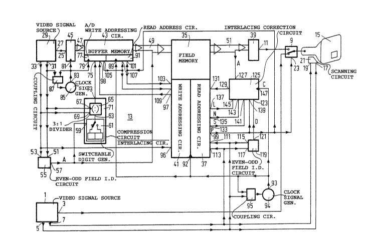
In Figure 1 a first video signal source 1 supplies a
first video signal from an output 3, a first horizontal
2a
. .~ ,
4~1
PHN 11.776 3 20-02-1987
synchronizing signal from an output 5 and a first vertical
synchronizing signal from an output 7. The first video signal
source 1 may be, for example, a receiver section of a
television receiver, a television camera or a video recorder.
The first video signal is applied from the output 3
of the first video signal source 1 to an input of a sub-
picture change-over switch 9 which receives at another input
a sub-picture signal obtained from an output 11 of a
compression circuit 13. An output of the sub-picture change-
10 over switch 9 applies a video signal to be displayed to a
picture display tube 15.
For the sake of clarity the Figure shows the
relevant signal paths in a single form. It will be evident
that multiple signal paths are used in a colour television
picture display device.
The first horizontal sychronizing signal and the
first vertical synchronizing signal are applied from the
outputs 5 and 7 of the first video signal source 1 to inputs
17 and 19, respectively, of a scanning circuit 21 which,
20 together with the first video signal provides for a main
picture display on the picture display tube 15.
For the display of a sub-picture the sub-picture
change-over switch 9 is periodically switched to the state
not shown during a part of each field period of the main
25 picture by a switching signal applied to an operating signal
input 23 of the sub-picture change-over switch 9.
The compression circuit 13 has an input 25 which
receives a second video signal from an output 27 of a second
video signal source 29. The second video signal source 29
30 also applies a second horizontal synchronizing signal to an
output 31 and a second vertical synchronizing signal to an
output 33. The second video signal source 29 may be, for
example, a possibly second receiver section of a television
receiver, a television camera or a video recorder.
The compression circuit 13 comprises a field memory
35 having a read circuit constituted by a read addressing
circuit 37 and a digital-to-analog converter 39 and a write
12~i8~48
PHN 11.776 4 20-02-1987
circuit comprising a write addressing circuit 41, a line
buffer memory 43 and an analog-to-digital converter 45. The
input 25 and the output 11 of the compression circuit 13 is
also the input of the analog-to-digital converter 45 and the
5 output of the digital-to-analog converter 39, respectively.
The analog-to-digital converter 45 applies via a signal path
47 a digitalized second video signal to the line buffer
memory 43 which supplies a digital second video signal via a
signal path 49 to the field memory 35, which video signal is
10 suitable to be written into this memory. The field memory 35
then applies a compressed digital second video signal via a
signal path 51 to the digital-to-analog converter 39 which
forms the sub-picture signal therefrom and supplies this
signal from its output 11.
The outputs 31 and 33 of the second video signal
source 29 are connected to inputs 51 and 53, respectively, of
a first even-odd field identification circuit 55 an output 57
of which supplies even-odd field information in the form of a
logic one or a logic zero signal dependent on the fact
20 whether the second video signal at the output 27 of the
second video signal source 29 originates from an even or an
odd field. This even-odd field information is applied vla the
signal path 49 to the field memory 35 and continuously
written therein. An even field is herein to be understood to
25 mean the picture field located in a high position and an odd
field is to be understood to mean the picture field located
in a low position of a frame. These fields will hereinafter
also be referred to as first and second fields, respectively.
The even-odd field identification circuit may be formed, for
30 example, in known manner or it may be of a type as described
in Netherlands Patent Application 8601062 (PHN 11.733).
The output 57 of the first even-odd field
identification circuit 55 is also connected to an operating
signal input 59 of a switchable digit generator 61 supplying
35 the digit one during one field and the digit two during the
other field to a count-write input 63 of a three-to-one
divider 65 which is formed as a counter and a counting signal
- ~268~8
PHN 11.776 5 20-02-1987
input 67 of which is connected to the output 31 for the
second horizontal synchronizing signal, whilst a write
command signal input 69 is connected to the output 33 for the
second vertical synchronizing signal from the second video
signal source 29. The digit generator 61 and the thxee-to-one
divider 65 constitute an interlacing circuit 71 whose output
73 connected to an output of the three-to-one divider 65
supplies a pulse to an input 75 of a write addressing circuit
77 of the line buffer memory 43 each time at the commencement
10 of a line to be written into said line buffer memory.
Likewise as a clock signal input 81 of the analog-
to-digital converter 45, a write clock signal input 79 of the
write addressing circuit 77 of the line buffer memory 43 is
connected to an output 83 of a first clock signal generator
85 whose frequency is coupled to that of the second
horizontal synchronizing signal by means of a coupling
circuit 87.
Likewise as a clock signal input 92 of the field
memory 35 and the write and read addressing circuits 41, 37
20 thereof, a read clock signal input 89 of a read address
circuit 91 of the line buffer memory 43 is connected to an
output 93 of a second clock signal generator 94 which, by
means of a coupling circuit 95, is coupled in frequency to
the first horizontal synchronizing signal originating from
25 the output 5 of the first video signal source 1.
The active field period in which the field memory 35
is written via the line buffer memory 43 is derived by the
write addressing circuit 41 of the field memory 35 from the
second vertical synchronizing signal applied to an input 96
30 thereof and originating from the output 33 of the second
video signal source 29. A signal representing this active
field period is applied by an output 97 of the write
addressing circuit 41 of the field memory 35 to an input 98
of the write addressing circuit 77 of the line buffer memory
35 43.
When the sub-picture is displayed the field memory
35 is not written from the line buffer memory 43. To this end
~` 32~
PHN 11.776 6 20-02-19~7
the switching signal, which is applied to the input 23 of the
sub-picture change-over switch 9 and which originates from an
output 99 of the read address circuit 37 of the field memory
35 and which will hereinafter be denoted by P, is also
applied to an interruption signal input 101 of the read
address circuit 91 of the line buffer memory 43 and to an
interruption signal input 103 of the write addressing circuit
41 of the field memory 35.
The line buffer memory 43 is written each time
10 during a line period of the seconcl video signal source 29
whereafter there is time during two line periods to transfer
its contents to the field memory 35 in the periods when there
is no display from the field memory 35. Transferring is
started immediately after writing. To this end a signal is
15 applied from an output 105 of the write addressing circuit 77
of the line buffer memory 43 to an input 107 of the read
address circuit 91 of the line buffer memory 43 and to an
input 109 of the write addressing circuit 41 of the field
memory 35.
The even-odd field information, hereinafter also
denoted by A, originating from the output 57 of the first
even-odd field identification circuit 55 is also applied to
the signal path 49 leading to the field memory 35 so that per
sample of the signal written into the field memory 35 a bit
25 is present which indicates whether the relevant sample
originates from an even or from an odd field of the second
video signal source 29. When the writing of the field memory
35 is organised in such a manner that it cannot be
interrupted at an arbitrary instant of a line period of the
30 second video signal source 29, as is indeed the case here, it
is sufficient to write the even-odd field information each
time at the commencement of a line period.
For the purpose of reading the field memory 35 the
read address circuit 37 thereof is synchronized with the
35 scanning circuit 21 of the picture display tube 15 via inputs
111 and 113 connected to the outputs 5 and 7; respectively,
of the first video signal source 1 so that the sub-picture is
~26~32~8
PHN 11 . 776 7 20--02-1987
displayed in a desired position in the main picture.
The outputs 5 and 7 of the first video signal source
1 also apply the first horizontal synchronizing signal and
the first vertical synchronizing signal to inputs 115 and
117, respectively, of a second even-odd field identification
circuit 119, from which synchronizing signals an even-odd
field information D of the main picture is derived which is
applied via an output 121 of the second even-odd field
identification circuit 119 to an input 123 of an interlacing-
lO correction circuit 125 a further input 127 of which receivesthe even-odd field information A of the sub-picture from the
signal path 51 during reading of the field memory 3~.
The interlacing-correction circuit 125 applies a
pulse via an output 129 thereof to an input 131 of the read
15 addressing circuit 37 of the field memory 35 at given
instants which will be further described hereinafter, which
pulse causes an address counter of this read address circuit
37 to make an extra step. This is the simplest manner of read
address correction. It is of course alternatively possible to
20 perform both positive and negative read address corrections.
This is, however, generally difficult to perform because
there are generally no connections on the address circuit
available for this purpose. The said pulse is derived from
the signals A and D by means of a number of signals P, S, N,
25 L which are obtained from outputs 99, 133, 135, 137,
respectively, of the read address circuit 37 of the field
memory 35 and which are applied to inputs 139, 141, 143, 145,
respectively, of the interlacing-correction circuit 125. A
clock signal input 147 of the interlacing-correction circuit
30 125 receives the second clock signal C from the output 93 of
the second clock signal generator 94.
The function of the above-mentioned signals and a
favourable embodiment of an interlacing-correction circuit
suitable for supplying the above-mentioned pulses for an
35 extra step of the read address circuit as defined above will
be elaborated with reference to Figure 2.
In Figure 2 corresponding components have the same
i8248
PHN 11.776 8 20-02-1987
reference numerals as in Figure 1 and the clock signal input
147 of the interlacing-correction circuit 125 is connected to
a clock signal input 151 of a field transition detection
circuit 153 which is connected to the clock signal input of a
5 D flip-flop 155 whose D input is connected via an input 157
of the field transition detection circuit 153 to the input
127 of the interlacing-correction circuit 125 for the even-
odd field information A of the sub-picture. The Q output of
the D flip-flop 155 applies a signal B to an inverting input
10 f an AND gate 159 which is delayed by one clock signal pulse
period with respect to the signal A. The other input of the
AND gate 159 is connected to the input 157 of the field
transition detection circuit 153, and the output of the AND
gate 159 is connected to an output 161 of the field
transition detection circuit 153. The AND gate 159 supplies a
pulse AB' from the output 161, which pulse covers one clock
signal period when there is an odd-even field transition. In
this case it was assumed that an even field of the sub-
pict~re corresponds to a value of the signal A which is logic
20 one and that the even field of the sub-picture is originally
located in a higher position than the odd field.
At an odd-even transition in the sub-picture the
displayed even portion would acquire a lower position after
the transition than the displayed odd portion before the
25 transition. To prevent this, the signal at the output 161 of
the field transition detection circuit 153 is applied to an
AND gate 163 a further input of which receives the signal P
from the input 139 and an inverting input is connected to the
input 141 to which the signal S is applied. The signal S is
30 high during a clock signal period at the commencement of the
sub-picture, consequently during the first clock signal
period of the signal P in a field of the main picture.
At an odd-even field transition, which occurs in the
sub-picture after the first clock period thereof, the AND
35 gate 163 supplies a pulse which is applied via an OR gate 165
and an OR gate 167 to the output 129 of the interlacing-
correction circuit 125 so that the read address of the field
. , .
:~L2~i8~4~3
PHN 11.776 9 20-02-1987
memory undergoes an extra increase of one step and the
portion of the sub-picture displayed after the odd-even
transition is raised in position and is brought to the
correct position with respect to the odd portion.
If the main picture field in which the sub-picture
occurred with the odd-even transition was an even field, the
next main picture field is odd and the sub-picture therein
will have an even~odd transition. The upper even portion of
the sub-picture is then positioned too low with respect to
10 the odd field of the main picture and is raised in position
by an extra step at the commencement of the sub-picture in
response to an extra pulse supplied by an AND gate 169
connected to a further input of the OR gate 165, whilst a
first input of said AND gate receives the signal S, a second
in2ut receives the signal A and a third inverting input
receives the signal D, i.e. the even-odd field information of
the main picture which is one when the relevant field of the
main picture is even.
If the main picture field in which the sub-picture
20 occurred with the odd-even transition was an odd field, the
next main picture field is an even field in which an even-odd
sub-picture transition takes place and in which the position
need not be corrected because the upper portions of the
fields have a correct location with respect to each other and
25 because there is no change of position at the sub-picture
field transition.
In principle the AND gates 163 and 169 and the field
transition detection circuit 153 may suffice.
The further components of the interlacing-correction
30 circuit of Figure 2 are refinements which perform additional
corrections in given cases.
To this end the field transition detection circuit
153 includes an AND gate 171 an input of which receives the
signal B from the Q output of the D flip-flop 155 and an
35 inverting input is connected to the input 157 of the
transition detection circuit 153. The output of the AND gate
171 is connected to an output 173 of the field transition
2~ 8
PHN 11.776 10 19-02-1987
detection circuit 153 and supplies a pulse during one clock
signal period in the event of an even-odd field transition of
the sub-picture.
The output 161 of the field transition detection
circuit 153 is also connected to an input of an AND gate 175
a second input of which is connected to the input 123 and a
third input of which is connected to the input 139 of the
interlacing-correction circuit 125.
The output 173 of the field transition detection
l0 circuit 153 is connected to a first input of an AND gate 177
an inverting second input of which is connected to the input
123 and a third input of which is connected tothe input 139
of the interlacing-correction circuit 125.
The outputs of the AND qates 17.5 and 177 are
15 connected to the input of an OR gate 179 the output of which
is connected to the set input of a set-reset flip-flop 181
the reset input of which receives the signal S from the input
141 of the interlacing-correction circuit 125 and the Q
output of which is connected to an input of an AND gate 183
20 the output of which is connected to the third input of the OR
gate 165. The clock signal input of the set-reset flip-flop
181 is connected to the clock signal input 147 of the
interlacing-correction circuit 125.
A second input of the AND gate 183 is connected to
2s the output of an OR gate 185 and a third input is connected
to the input 141 of the interlacing-correction circuit 125.
The inputs of the OR-gate 185 are connected to the
outputs of two AND-gates 187, 189. The inputs of the AND-gate
187 receive the signals A, D and P from the inputs 127, 123,
30 139, respectively, of the interlacing-correction circuit 125.
An input of the AND gate 189 is connected to the input 139 of
the interlacing-correction circuit 125 for the signal P and
its two inverting inputs are connected to the input 127 for
the signal A and to the input 123 for the signal D of the
35 interlacing-correction circuit 125.
The set-reset flipflop 181 is reset by the clock
signal each time at the trailing edge of the signal S so that
32~8
PHN 11.776 11 19-02-1987
this flipflop 181 can only apply a logic one signal to the
AND gate 183 until the end of the signal S when in the
previous field of the main picture the OR gate 179 had
supplied a logic one signal during the main picture. This is
5 the case due to the operation of the AND gate 175 when the
main picture field was even and when an odd-even field
transition had occurred in the sub-picture, or due to the
operation of the AND gate 177 when the main picture was odd
and when an even-odd field transition had occurred in the
10 sub-picture. The AND gate 183 can then supply a logic one
signal during the occurrence of the signal S at the
commencement of a sub-picture if also the OR gate 1B5
supplies a logic one signal, which is the case when the main
picture field and the sub-picture field are both even or both
15 odd. This only occurs when the field transition of the sub-
picture is displaced to the commencement thereof and is
located so close to the commencement thereof that no field
transition occurs in the sub-picture during the next field.
Due to this measure it is even possible to display in an
20 undisturbed manner a sub-picture originating from a 60 Hz
video signal source in a main picture of a 50 Hz video signal
source, or conversely.
In one of the above-mentioned cases the OR gate 165
thus applies a logic one signal to the OR gate 167, which
25 signal is also applied to an input 191 of a sub-picture end
correction circuit 193 which is also the set input of a set-
reset flipflop 195 whose Q output is connected to an input of
an AND gate 197 whose output 199 is also the output of the
sub-picture end correction circuit 193. A second input 200 of
30 the sub-picture end correction circuit 193, which is also the
clock signal input of the set-reset flipflop 195, receives
the clock signal from the input 147 of the interlacing-
correction circuit 125. A third input 201 of the sub-picture
end correction circuit 193, which is also the reset input of
35 the set-reset flipflop 195, receives the signal N from the
input 143 of the interlacing-correction circuit 125. This
signal N is a pulse which occurs in the clock signal period
~ ~;8~
PHN 11.776 12 20-02-1987
preceding the signal S, hence in the clock signal period
prior to the commencement of the sub-picture so that the set-
reset flipflop 195 is reset prior to the commencement of each
sub-picture.
A fourth input 203 of the sub-picture end correction
circuit 193 receives the signal L from the input 145 of the
interlacing-correction circuit 125. This signal L is a pulse
which occurs in the last clock signal period of the
penultimate line of the sub-picture. If during the occurrence
10 of the sub-picture there had been no set action of the set-
reset flipflop 195 because the OR gate 165 had not supplied
an address correction signal, the Q output of this set-reset
flipflop 195 is still logic one and the AND gate 197 as yet
applies a logic one signal to the output 199 of the sub-
15 picture end correction circuit at the end of the penultimateline of the sub-picture, which logic one signal produces an
address correction via the OR gate 167 so that the end of the
sub-picture occurs in the same position in the main picture
as in the cases when an address correction signal is supplied
20 by the OR gate 165 so that troublesome jumping of the end of
the sub-picture cannot occur
When the number of lines of the sub-picture is a
multiple of three, the interlacing circuit 71 can be formed
in a simpler manner by writing only once per two fields a
25 suitable value into the counter 65 via the count input 63.
It will be evident that if the first video signal of
the main picture is also digital, the digital-to-analog
converter 39 can be incorporated after the sub-picture
change-over switch 9, if desired, if the first and the
30 second video signal have the same digital structure.
The even-odd field identification circuits 55 and
119 may each form part, if desired, of for example a
synchronizing signal pattern correction circuit as described
in the previously mentioned Netherlands patent application
35 8601062, which circuits can then apply the relevant
synchronizing signals to the inputs 67 and 69 of the
interlacing circuit 71 and to the input 96 of the write
48
-
PHN 11.776 13 19-02-1987
addressing circuit 41 of the field memory 35 and to the
inputs 111 and 113 of the read addressing circuit 37 of the
field memory 35 and to the inputs 17 and 19 of the scanning
circuit 21, respectively.