Note: Descriptions are shown in the official language in which they were submitted.
~L~68~
PROCESS FOR THE PRODUCTION OF A PIEZORESISTIVE GAUGE
.....
AND TO AN ACCELEROMETER INCORPORATING SUCH A GAUGE
BACKGROUND OF THE INVENTION
The present invention relates to a process for the
production of a piezoresistive strain gauge on one
lateral face of a flexible beam more particularly
belonging to a directional acce:Lerometer, as well as to a
process for producing a d:irectional accelerometer
equipped with a piezoresistive gauge. These processes
use microelectronics technology.
In general terms, an accelerometer essentially comprises
a moving mass m and means making it possible to measure
the force F=m.A due to the acceleration A of a moving
body. A directional accelerorneter produced on the basis
of microelectronics technology is described in FR-A-2 558
263 in the name of the present Applicant.
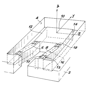
Fig 1 shows in perspective part of the accelerometer
described in the aforementioned document. This
accelerometer comprises a parallelepipedic substrate 2
having a recess 4 completely traversing the substrate.
In said recess are located two parallelepipedic flexible
beams 6, 8, whose thicknçss is much greater than the
width (typically 30 times greater). These beams are
oriented in a direction Y parallel to the surface of the
substrate. These beams have a fixed end integral with
substrate 2 and a free end supporting a parallelepipedic
block 10.
The displacement of block 10 in direction x is measured
with the aid of capacitive detectors, defined by
conductive deposits on the lateral faces 12, 14 of block
10 and on the walls of recess 2 facing said faces 12, 14.
This solution has the advantage of being easily brought
about according to microelectronics technology. However,
these capacitive detectors suffer from a certain number
B 9095.3 LC
~Z6BZ~i6
--2--
of disadvantages. In particular, they are very sensitive
to parasitic capacitances, have a high internal impedance
and a non-linear response. Moreover, they have an
important influence on the electrostatic forces produced
in the accelerometer.
Beams 6 and 8, as well as block 10 are monoblocks and
defined by anisotropic etching of substrate 2. They
constitute the seismic or moving mass of the
accelerometer. Beams 6 and 8 can deform, leading to a
displacement of block 10, in a direction x parallel to
the surface of the substrate and perpendicular to
direction y, said direction x corresponding to the
direction of the component of the acceleration to be
measured.
The use of piezoresistive strain gauges deposited on the
beam of said accelerometer would make it possible to
solve the disadvantages associated with capacitive
sensors.
It is pointed out that a piezoresistive strain gauge is a
conductive strip, whose resistance varies with the
deformations of the beam on which it is located. This
solution was envisaged in the aforementioned document.
The gauges associated in pairs and designated 15 and 17
in fig 1 are resistors disposed on the upper face of the
beams, which is the only face accessible by conventional
micrography processes.
Unfortunately, in this type of accelerometer, the aim is
to have a much greater flexibility in direction x
(parallel to the surface of the substrate in which the
accelerometer is formed and perpendicular to the
longitudinal direction of beam y) than in direction y.
However, these beams typically have a width of 3 to 10
micrometers for a thickness of a few hundred micrometers.
B 9095.3 LC
~6~Z66
In view of the fact that very little space is available
for positioning strain gauges on the upper surface of the
beams, serious technical problems are caused by the
construction of said gauges.
This is made worse by the fact that strain gauges cannot
be positioned along the median longitudinal axis y of
beams because on the neutral fibre 16 of the beams, the
deformation in direction z perpendicular to the substrate
surface is zero. Furthermore, these strain gauges can
also not be positioned over the entire length of the beam
because, on average, the deformation is zero.
This problem can be solved by utilizing strain gauges of
the type shown in fig 1 located at both ends of the
beams. However, on adding the current supply conductors
for these gauges, serious technological problems occur
due to the very small dimensions of the elements of the
accelerometer. Moreover, assuming that such a structure
can be produced, there would still be the problem of heat
dissipation, in view of the fact that the gauges only
occupy a very small surface on the upper face of the
beams.
In view of the problems concerning the available space on
the upper face of the beams, the inventors have
considered depositing strain gauges on the lateral faces
~5 of the beamst oriented parallel to direction y and
perpendicular to direction x of detection of an
acceleration. Unfortunately, the conventional
microelectronics processes using etching masks or
deposits parallel to the surface of the substrate do not
make it possible to accurately define patterns on the
faces perpendicular to the substrate (lateral faces of
the beams).
B 9095.3 LC
~L~6~ 616
SUMMARY OF THE INVENTION
The present invention is directed at a process for the
production of a piezoresistive strain gauge located on a
lateral face of a flexible beam, especially of an
accelerometer, produced according to microelectronics
technology.
More specifically, the invention relates to a process for
the production of a piezoresistive gauge on a lateral
face of a beam formed by etching a substrate
perpendicular to its surface and having and end which can
move laterally in a first recess defined in the substrate
comprising the stages of etching the substrate
perpendicular to its surface for forming a second recess
communicating with the first, the communication zone
representing the image of the gauge to be produced,
placing on the substrate surface of a mechanical mask
having an opening facing the second recess and partly
extended over the upper face of the beam, passing through
said opening a particle beam able to form a
piezoresistive layer constituting the gauge and electric
contacts, said beam being oriented obliquely with respect
to the substrate surface, elimination of the mask and
producing electrical conductors on the upper and lower
faces of the beam with a view to supplying the gauge with
electric current.
This production process is easy to perform.
The piezoresistive gauge can be formed by depositing a
piezoresistive material by vacuum evaporation or, in the
case of a silicon substrate, by implanting ions, e.g. of
boron or phosphorus.
When the piezoresistive gauge is evaporated, it is
preferably made from polycrystalline germanium doped
with several % of gold. Such a material makes it
B 9095.3 LC
- ~26~26~
--5--
possible to obtain an ade~uately high transverse gauge
coefficient Kt. The transverse coefficient of a gauge is
defined in the present case by (~ sy/sy)/( ~z/z1 with
~sy/sy representing the conductivity variation along axis
y and ~z/z the deformation of the beam along axis z.
The current supply conductors can be deposited on the
surface of the beam either before etching the substrate,
or after depositing the piezoresistive gauge. The
electrical conductors can be deposited in advantageous
manner by vacuum evaporation.
The invention also relates to a process for producing an
accelerometer having a piezoresistive gauge obtained as
hereinbefore and wherein the first and second recesses
are simultaneously formed by etching the substrate
perpendicular to its surface.
Advantageously the first and second recesses are formed
by anisotropic chemical etching of the substrate.
BRIEF DESCRIPTION OF THE ~RAWINGS
The invention is described in greater detail hereinafter
relative to non-limitative embodiments and the attached
drawings, wherein show :
Fig 1, already described, part of a directional
accelerometer produced according to microelectronics
technology.
Fig 2, in perspective, the inventive strain gauge
production process.
Fig 3, in perspective, the production of power supply
conductors for a piezoresistive gauge produced according
to the process of the invention, the conductors being
formed a~ter the gauge.
Fig 4, in perspective, a flexible beam equipped with a
piezoresistive gauge and power supply conductors produced
in accordance with the inventive process, the conductors
being produced before the gauge.
~268Z~
--6--
Figs 5 to 10, in perspective, the production of an
accelerometer with a piezoresistive gauge in which the
power supply conductors are produced before the gauge,
figs 5 and 6 relating to a quartz substrate and figs 7 to
10 to a silicon substrate.
DETAILED DESCRIPTION OF THE INVENTION
The following description relates to the production of a
strain gauge placed on a lateral face of an accelerometer
beam produced in accordance with microelectronics
technology. However, the invention can obviously also be
used for simultaneously producing several piezoresistive
gauges. In the case of an accelerometer having two
flexible beams, there can be four piezoresistive gauges
connected as a Wheatstone bridge. In order to ensure a
good stability of the bridge, the gauges can be
simultaneously deposited in pairs.
Fig 2 is a perspective view of part of an accelerometer
which is to be equipped with a piezoresistive strain
gauge produced according to the inventive process. This
accelerometer comprises a monocrystalline quartz or a
silicon substrate 22 having a first recess 24 completely
traversing substrate 22, in which is located a flexible
beam 26 shaped like a rectangular parallelepiped. Beam
26 has a thickness which is 30 times greater than its
width and is oriented in a direction y parallel to the
substrate surface. It has a free end able to move in a
direction x perpendicular to direction y and parallel to
the surface of the substrate under the action of an
acceleration directed in said direction x. The other end
of the beam is integral with substrate 22.
Beam 26 is obtained by etching substrate 22 perpendicular
to its upper surface 27 in an anisotropic manner and by
the chemical route using an appropriately shaped mask
located on the upper surface 27 of the substrate.
B 9095.3 LC
-` ~2~ 6~
--7--
In order to deposit a piezoresistive gauge on a lateral
face 28 of beam 26, the substrate is etched perpendicular
to its surface 27, in order to form a second recess 30
communicating with the first recess 24. This
anisotropically performed etching can be carried out by
the wet chemical route.
Etching take place through an appropriately shaped mask
made from a good conductive material, such as a gold
layer on a chromium layer and located on the upper
surface 27 of the substrate. Moreover, said etching is
performed over the entire thickness of substrate 22.
The second recess 30 which, in fig 2, is shaped like a C,
is linked with the first recess 24 by an opening 32
formed in the substrate and representing the image of the
gauge to be produced on the lateral face 28 of the beam.
In particular, the width 1 of opening 32 defines the
width of the gauge to be produced on the lateral face 28
of beam 26.
Above the upper surface 27 of substrate 22 is then placed
a mechanical mask 34 making it possible to define the
dimensions of the electric contact zone of the gauge to
be produced on the upper face 36 of the beam.
For this purpose, mask 34 has a rectangular opening 38
located above the second recess 30 of opening 32 and
partly extended over the first recess 24 and the upper
face 36 of beam 26. The width L of opening 38 of the
mask preferably exceeds the width 1 of opening 32 made in
the substrate and facing the gauge to be produced.
By using mask 34 and the slot 30-32 made in substrate 22
as the mask, beam 26 is exposed to a particle beam 40
able to form a deposit 42 of a piezoresistive material
constituting the gauge and its electric contacts.
B 9095.3 LC
~261~6Gi
--8--
A polycrystalline germanium deposit 42 doped with several
% of gold (5 to 10%) can be obtained with the aid of a
gold and germanium atom beam 40. This material makes it
possible to obtain a sufficiently high transverse gauge
S coefficient Kt. Advantageously, the piezoresistive gauge
is deposited by vacuum evaporation at a rate of
approximately 1 nm/s.
Preferably, the particle beam 40 is directed onto the
lateral face 28 of the beam in accordance with a glancing
incidence. In other words the beam 40 forms an angle A
with the upper surface 27 of substrate 22. This angle is
dependent on the thickness of mask 34, the dimensions of
the mask opening 38 and the distance d separating the
face 28 of beam 26 and the lateral face of recess 24
facing the same.
o o
It varies between 10 and 30 and is typically 20 for
a 0.15 mm thick mask 34, so as to have a piezoresistive
deposit 42 having an adequate thickness and having a
lateral portion 44 constituting the actual piezoresistive
gauge, located on lateral face 28 and extending over the
entire thickness of the beam and portions such as 46
respectively covering the upper and lower faces 36, 48 of
beam 26 defining the electric contact zones of the gauge.
This inclination also makes it possible to avoid an
exaggerated covering of beam portion 44.
This is followed by the formation of the electrical
conductors for supplying current to the piezoresistive
gauge 44, said conductors clearly resting on contacts 46.
As shown in fig 3, these conductors are deposited on the
upper and lower faces 36, 48 of beam 26. The current
supply conductor, e.g. produced on the upper face 36 of
the beam is designated 50 and the current outflow
conductor, e.g. placed on the lower face 48 of the beam
B 9095.3 LC
-
~Z6~3Z66
g
is designated 52.
These conductors 50 and 52 are deposited by vacuum
evaporation using mechanical mask 34 and slot 30-32 of
the substrate as a mask during evaporation. The
corresponding particle beam 51 forms an angle B with the
upper surface of the substrate. This angle is chosen in
such a way that the lateral face 54 of the beam, opposite
to face 28, is only partly covered with the conductive
deposit so as not to short-circuit the gauge, angle s
e.g. being between 30 and 60 . Conductors 50 and 52
are in particular made from gold or aluminium.
As shown in fig 4, it is also possible to produce the
electrical conductors 50a and 52a of piezoresistive gauge
44a, respectively disposed on the upper and lower
surfaces 36, 48 of the beam 26 before producing the said
gauge 44a and its electric contacts 46a, as described
with reference to fig 2.
With reference to figs 5 and 6, a description will now be
provided of the production of an accelerometer with a
piezoresistive strain gauge in which the power supply
conductors of the gauge are made before the latter, the
substrate being of quartz.
Two conductive layers 56, 58 are formed by vacuum
evaporation on respectively the entire upper and lower
faces 27, 29 of a quartz substrate 22. These layers 56
and 58 are e.g. formed by a gold layer on a chromium
layer.
On layers 56 and 58 are then respectively formed two
resin masks, each representing the image of the flexible
beam 26 of the accelerometer (fig 4), first and second
substrate recesses and through said masks there is a
first chemical etching of layers 56, 58 (fig 5), followed
B 9095.3 LC
~26~66
- 1 0 -
by the elimination of the two etching masks.
One of the thus etched conductive layers 56, 58 will
subsequently serve as an etching mask for substrate 22.
On the etched layers 56, 58 are then again formed two
resin masks 60, 62 representing the image of the power
supply conductors, respectively 50a and 52a (fig 4) to be
produced.
As shown in fig 6, this is fo:Llowed by an anisotropic
chemical etching of substrate 22 e.g. using etched layer
56 as the mask. This etching of the substrate is
effected perpendicular to its upper surface 27 (direction
z), in order to form the first and second recesses 24, 30
respectively and the flexible beam 26 of the
accelerometer. Moreoverr said etching is performed over
the entire thickness of the substrate.
Using resin masks 60, 62, there is then a second etching
of layers 56, 58 in order to form the power supply
conductors 50a, 52a (fig 8) for the piezoresistive gauge.
After the elimination of masks 60, 62 on the upper
substrate face 27 is e.g. placed the mechanical mask 34
making it possible to define the lateral dimensions of
the gauge. As described relative to fig 2, this is
followed by the deposition of the piezoresistive gauge
and its electric contacts by vacuum evaporation on faces
28, 36 and 48 of beam 26.
A resistance of approximately 6k.ohm is obtained with a
polycrystalline germanium piezoresistive gauge doped with
10% of gold having a width (equal to l) of 50
micrometres, a length (equal to the substrate thickness
and therefore of the beam) of 150 micrometres and a
thickness of 0.2 micrometre. Using a Wheatstone bridge
of four gauges produced in the manner defined
B 9095.3 LC
`` lZ6~3~6~
hereinbefore on monocrystalline quartz beams and a beam
deformation of 0.5,10 , an accelerometer is obtained
supplying a signal of 7.5 mV per supply volt. This
compares with 3 mV per supply volt obtained with
conventional accelerometers.
Figs 7 to 10 show the production of an accelerometer with
piezoresistive strain gauge in which the power supply
conductors are still produced prior to the gauge, but in
which the substrate is made frorn silicon.
Compared with the process described relative to figs 5
and 6, between substrate 22 and respectively conductive
layers 56, 58 are placed two insulating layers 64, 66
made from Si N4 and/or SiO2 and deposited by CVD
(chemical vapour phase deposition) or thermal oxidation
for SiO .
After the formation of a resin mask on each of the
conductive layers 56, 58 representing the image of the
flexible beam and first and second substrate recesses,
there is a first etching of conductive layer 56, 58 and
then insulating layers 64, 66 ~ig 7), after which these
masks are eliminated.
The insulating layers 64 or 66 etched in this way will
subsequently serve as an etching mask for substrate 22.
This is followed by the formation of masks 60, 62
representing the image of the power supply conductors
50a, 52a (fig 8) to be produced.
In the manner shown in fig 8, this is followed by a
second etching of conductive layers 56, 58 to form the
supply conductors and then masks 60 and 62 are
eliminated.
For example, using the etched insulating layers 64, 66
B 9095.3 LC
32~i6
-12-
as the mask, there is an anisotropic chemical etching of
substrate 22 over the entire thickness thereof and in
direction z perpendicular to the upper substrate surface
27. This makes it possible to Eorm the first and second
5recesses 24, 30 respectively and the accelerator beam 26.
According to fig 9, there is then a second chemical
etching of insulating layers 64, 66 respectively using
conductors 50a and 52a as a maslc.
Mechanical mask 34 is then placed on the upper surface 27
of the substrate and boron or phosphorus ions are then
implanted through said mask in order to form, in the
faces 28, 36 and 48, a piezoresistive layer 42a
constituting the gauge and its electric contacts. The
inclination of the ion beam 40 is between 10 and 30 ,
in order to prevent any ion implantation in the lateral
face 54 (fig 10) of beam 26 opposite to face 28.
A second implantation in accordance with angle B (fig 2)
can optionally be carried out with a view to obtaining a
greater doping of the upper and lower faces of the beam.
As shown in fig 10, this is followed by the formation of
two conductive deposits 68, 70, e.g. of aluminium, on
and below beam 26 permitting the electrical connection of
implanted layer 42a to both the upper conductor 50a and
to the lower conductor 52a.
In the case of a silicon substrate with flexible beams 26
obtained by anisotropic chemical etching, the lateral
faces and in particular face 28 of the beam must be
plains (111) of the silicon, so that the transverse gauge
coefficient Kt is in this case close to 30, independently
of the direction of the gauges. Under such conditions,
the output signal of an accelerometer equipped with four
implanted gauges, connected as a Wheatstone bridge, is
B 9095.3 LC
-13_ ~ ~ ~ 8 26 6
approximately 15 mV per supply volt, which is once again
appropriate.
B 9095.3 LC