Note: Descriptions are shown in the official language in which they were submitted.
8~t~
BACKGROUND OF THE INVENTION
Field of the Invention
The present invention relates to a tuned oscillator
for being used as a local oscillator for a tuner of a radio
receiver, a television receiver and so on, a sweep oscillator
for a spectral analyzer, a microwave measuring instrument and
so on.
Description of the Prior Art
As a tuned oscillator, there is previously proposed
such one which uses an YIG (where YIG represents yttrium, iron
and garnet but it may contain various kinds of additives)
single crystal sphere (as is disclosed in a published examined
Japanese patent application No. 32671/1973). This YIG sphere
has various features such as the Q value of resonance charac-
teristic high in the microwave band; it can be constructed
small in size because its resonance frequency is independent
on the volume of the YIG; the resonance frequency thereof can
be varied linearly in a wide band by changing a blas magnetic
field applied to the YIG sphere; and so on.
However, the above-described tuned oscillator has a
defect that due to the YIG sphere used therein, the tuned
oscillator is difficult to be integrally formed on an MIC
(thin film hybrid microwave integrated circuit) substrate
and hence its construction flexibility is restricted.
Further, this YIG-tuned oscillator has disadvantages that the
coupling tightness must be matched by adjusting lead wires or
ribbons constituting a coupling loop of the YIG sphere and by
adjusting the position between the coupling loop and the YIG
12688;~7
sphere and that this tuned oscillator is easily affected by
vibration.
OBJECTS AND SU ~RY OF THE INVENTION
It is an object of the present invention to
provide an improved tuned oscillator utilizing ferromagnetic
resonance.
It is another object of the present invention to
provide a tuned oscillator having an uniform characteristics.
It is a further object of the present invention
to provide a tuned oscillator having a simple construction
and being suitable for making the same small in size.
According to one aspect of the present invention
there is provided a tuned oscillator which comprises:
an active element; and
a ferromagnetic resonator connected to said active
element;
said ferromagnetic resonator being formed of a ferri-
magnetic crystal, a microstrip line magnetically
coupled to said ferrimagnetic crystal and D.C. bias
magnetic field means applying D.C. bias magnetic field
to said ferrimagnetic crystal, said ferrimagnetic
crystal being formed of an YIG thin film formed by
thin film forming technique and being processed to
suppress magnetostatic mode of ferromagnetic resonance
other than uniform mode.
The other objects, features and advantages of the
present invention will become apparent from the following
description taken in conjunction with the accompanying
-- 3
8~
drawings through which the like references designate the
same elements and parts.
BRIEF DESCRIPTION OF THE DRAWINGS
Fig. 1 is a cross-sectional view illustrating an
embodiment of a tuned oscillator according to the present
invention;
Fig. 2 is a plan view showing a practical
structure of the oscillating circuit;
Fig. 3 is a cross-sectional view taken along a
line A-A in Fig. 2;
Fig. 4 is a block diagram useful for explaining
the oscillating circuit;
Fig. 5 is a circuit diagram showing an example
of the oscillating circuit;
Fig. 6 is a Smith chart useful for explaining
the oscillation operation;
Figs. 7, 8, 9, 12, 13, 14, 15 and 17 are respec-
tively diagrams useful for explaining the present invention;
Figs. 10 and 16 are respectively perspective views
illustrating examples of an YIG thin film magnetic resonance
elements;
Fig. 11 is a cross-sectional view of Fig. 10; and
Figs. 18 to 25 are respectively diagrams showing
other embodiments of the oscillating circuits according to
the present invention.
- 4 -
~6~
DESCRIPI'ION OF THE PREFERRED EMBODIMENTS
.
Now, an embodiment of the tuned oscillator
according to the present invention will hereinafter be
described with reference to the drawings.
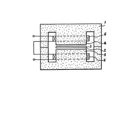
In this embodiment, as shown in Fig. 1, there
is provided a yoke 1 made of magnetic material such as ferrite
and so on in which a magnetic gap 2 is formed. In the
magnetic gap 2, there is located a substrate 3 which in~
corporates therein an oscillating circuit. A coil 6 is
wound around at least one of magnetic poles 4 and 5 which
are opposed to each other to constitute the magnetic gap 2
of the yoke 1 and a variable current is supplied to the coil
6, thus variable magnetic field applying means being formed.
Fig. 2 is a plan view illustrating an example of
the practical construction of the substrate 3 which incorpo-
rates therein the oscillating circuit and Fig. 3 is a
cross-sectional view taken along a line A-A in Fig. 2. As
shown in Figs. 2 and 3, a ground conductor 32 is formed on
a first major surface of a dielectric substrate 31 made of
a material such as alumina and so on. A microstrip line 33
is formed on a second major surface of the dielectric sub-
strate 31, one end of which is connected through a conductor
34 to the ground conductor 32. The microstrip line 33 is
electromagnetically coupled with an YIG thin film magnetic
resonance element 35. The YIG thin film magnetlc resonance
element 35 is formed as follows. An YIG thin film of ferri-
magnetism material is formed on one major surface of, for
example, a GGG (gadolinium gallium garnet) substrate 36 by a
thin film forming technique such as sputtering, chemical
~68~3~7
vapor deposition method (CVD method), liquid phase epitaxial
growth method ~LPE method) and so on and this YIG thin film
is shaped as, for example, a disk shaped pattern by photo-
lithography technique. In Figs. 2 and 3, reference numeral
37 designates a high frequency bipolar transistor, reference
numeral 38 designates an impedance matching circuit and
reference numeral 39 designates a DC blocking MOS (metal
oxide semiconductor) capacitor thereof. In this embodiment,
the base B of the bipolar transistor 37 is connected to a
ground pad 40 connected to the ground conductor 32 through
a wire 41 which forms a reactance. The emitter E thereof is
connected to the side of the YIG thin film magnetic resonance
element 35 and the collector C thereof is connected to the
side of the impedance matching circuit 38, thus a so-called
common base series feedback oscillator being formed.
An explanation will be given on the oscillation
principle, the oscillation condition and so on of the
oscillating circuit using the YIG thin film magnetic resonance
element 35 as its resonator. The oscillating circuit in
which the resonator or the YIG thin film magnetic resonance
element 35 is inserted into a feedback circuit other than an
output circuit will be described. Figs. 4A and 4B are
respectively block diagrams showing this oscillating circuit.
In Figs. 4A and 4B, reference numeral 42 designates an YIG
thin film resonance circuit, reference numeral 43 designates
a negative resistance circuit, reference numeral 44
designates an impedance matching circuit and reference
numeral 45 designates a load. In Fiy. 4B, reference numeral
46 designates a load impedance which includes the impedance
matching circuit.
~L~68~3~7
In Fig. 4, respective reflection coefficients ry
and rN seen to the YIG thin film resonance circuit side or,
namely, the YIG feedback circuit side and to the active
element side, namely, the negative resistance circuit side
from a terminal A are respectively expressed by the follow-
ing equations using their impedances Zy and ZN seen from
the terminal A.
r = ZY o -- (1)
10 Zy + Zo
r = ZN - -Z ... (2)
N 0
where Z0 is the characteristic impedance (50 Q) of the
circuit.
The stationary oscillation condition is expressed
using the impedances ry and rN as
ryrN = 1 -- (3)
Since the impedances ry and rN are both complex
numbers, Eq. ~3) can be rewritten to the following equation
if it is separated to the amplitude and phase
Iryl IrNIe Y N = 1
namely
lry-l IrNl = 1 ... (a~)
~y + eN = -- (5)
Since the YIG feedback circuit as a passive element
1268~c:7
circuit has a positive effective resistance corresponding
to the loss of the YIG thin film resonator, Eq. (1) yields
¦ ry I < 1 . Accordingly, to establish the oscillation
condition given by Eq. (4), the condition of ¦rNI > 1 must
be established and thence from Eq. (2), it is understood
that the impedance ZN is required to have a negative
effective resistance.
While the negative resistance circuit 43 in Fig.
4 may be a 2-terminal active element serving as a negative
resistance element or combination of a circuit made of a
3-terminal active element and feedback element, in the
example shown in Figs. 2 and 3, the high frequency bipolar
transistor of a 3-terminal active element is used and is
formed as the common base series feedback type oscillating
circuit as shown in Fig. 5. In Fig. 5, reference letter X
designates a reactive circuit.
Although the stationary oscillating condition of
the oscillating circuit was described so far, the following
condition must be established so as to cause the oscillating
circuit to oscillate.
Iryl IrNSI > 1 - (6)
namely
Iryl > 1 -- (7)
where rNs is the value of rN in a small signal. When the
oscillating circuit begins to oscillate and the active
element be~nsc to operate with a large amplitude, the
absolute value of the negative resistance becomes small and
1/ IrN¦ becomes large gradually. When Eq. (2) is established,
the oscillation of the oscillating circuit becomes a
stationary state.
On the basis of the above-described explanation,
the operation principle of the YIG oscillating circuit will
be described with reference to a Smith chart of Fig. 6.
As illustrated in Fig. 6, while under the state
of the signal with small amplitude, 1/ rN iS in the state
on a curve C which is relatively near the inside of the Smith
chart, it passes the state shown by a curve D and moves in
the direction shown by arrows as the active element operates
with a large amplitude.
In the YIG oscillating circuit described before in
connection with Figs. 2 and 3, when the YIG thin film
magnetic resonance element 35 does not resonate, it becomes
a mere strip line with the tip end short-circuited so that
ry subtends a locus as shown by A in Fig. 6. As wil] be
clear from Fig. 6, the phase condition for the oscillation
as given by Eq. (5) is not satisfied by the reflection coef-
ficient rN having any amplitude and thus no oscillation is
caused.
If the YIG thin film magnetic resonance element 35
is applied with a DC magnetic field so as to resonate at a
frequency f0 between frequencies fl and f2, with a frequency
near the frequency f0, the reflection coefficient ry draws
a lccus as shown by B in Fig. 6. At this time, at a frequency
near the frequency f0, the amplitude condition given by Eq.
(7) and the phase condition given by Eq. (5) for starting the
oscillation are established at the same time. When the
oscillation is started and 1/ rN moves from the curve C to
the curve D in Fig. 6, Eqs. (4) and (5) are established at
g
~.~68~t7
the same time at the frequency fO so that the oscillating
circuit stationarily oscillates at the oscillation frequency
fo
If, under this principle, the resonance frequency
of the YIG thin film element 35 is varied in a range from f
to f2 by varying DC magnetic field applied thereto, the
oscillating circuit oscillates in tune with a frequency near
the resonance frequency.
In this embodiment, the resonator is formed of the
YIG thin film magnetic resonance element which is formed by
the thin film forming techni~ue. In this case, it is desired
to suppress a spurious response caused by magnetostatic modes.
More specifically, the magnetic resonance element (YIG single
crystal sphere) made of a single crystal sphere has an
advantage that the magnetostatic mode is difficult to be
excited and the sole resonance mode by uniform precession
mode can be obtained. The magnetic resonance element made
of the YIG thin film has, on the other hand, a defect that
even if it is located in a good uniform RF magnetic field,
magnetostatic mode is excited much because the internal DC
magnetic field is not uniform. Magnetostatic modes presented
when a DC magnetic field is perpendicularly applied to the
surface of a disc-shaped sample made of ferrimagnetic material
are analyzed on a literature (journal of Applied Physics, Vol
48, July 1977, pp. 3001 to 3007) in which each mode is
indicated as (n, N)m scheme. The (n, N)m mode has n nodes
in the circumferential direction thereof, N nodes in the
radius direction thereof and (m - 1) nodes in the thickness
direction thereof. When th~ uniformity of the RF magnetic
field through the sample is excellent, (1, N)l series becomes
-- 10 --
'7
a main magnetostatic mode. Fig. 7 shows measured results
of ferromagnetic resonance of a disk-shaped YIG thin film
sample measured in a cavity resonator operating at the
frequency of 9 GHz, in which magnetostatic modes of (1, N)l
series are excited significantly. When the above-described
microwave element such as the filter and the like are con-
structed by using this sample, magnetostatic mode of (1, 1)
which is the uniform mode is used and at this time other
magnetostatic modes all cause a spurious response. Thus
there occurs such a fear that a spurious oscillation and mode
jump are caused. Therefore, it is desired for each magnetic
resonance element made of ferrimagnetism material thin film
for example YIG thin film to provide means which suppress the
excitation of the magnetostatic modes which will become the
spurious response without deteriorating the uniform mode.
This will be described next.
Fig. 8 shows the state of an internal DC magnetic
field Hi when a DC magnetic field is applied to the YIG
disk-shaped thin film with a thickness t and a diameter D
(radius R) in the direction perpendicular to its surface.
In this case, its aspect ratio t/D is sufficiently small and
a magnetic field distribution in the thickness direction of
the sample is neglected. Since the demagnetizing field is
large in the inside of the disk and becomes suddenly smaller
in its outer periphery so that the internal DC magnetic
field is small near the center thereof and becomes suddenly
large near the outer periphery thereof. ~ccording to the
analyzed results of the afore-described literature, if a
value of r/R at the position where Hi = ~/~ is taken as ,
the magnetostatic mode lies in the region of 0 ~ r/R ~
~L2~8~
where ~ is the resonance angular frequency at the magnetostatic
mode and y is the gyromagnetic ratio. When the magnetic field
is fixed, the resonance frequency is increased as the mode
number N becomes large so that the region of the magnetostatic
mode is extended gradually to the outside as shown in Fig. 9A.
Fig. 9B shows distributions of RF magnetization, of the sample
with respect to three lower-order modes of the (1, N)l mode
where the absolute value represents the magnitude of the RF
magnetization and the reference designates the phase relation
of the RF magnetization. As is clear from Fig. 9, since the
RF magnetization becomes different in the magnetostatic modes,
if this is utilized, it becomes possible to suppress the
excitation of the magnetostatic mode which will become the
spurious response without substantially affecting the uniform
mode.
Practically, as shown in Fig. 10, an annular groove
53 is formed by, for example, a selective etching technique
on an YIG thin film magnetic resonance element 52 of, for
example, a disc shape which is formed on a GGG substrate 51
to thereby provide an annular thin portion. In this case,
the YIG thin film magnetic resonance element 52 is made suf-
ficiently small in thickness and the magnetostatic mode in
this case is (1, N)l mode.
The groove 53 is formed concentrical with the
element 52 at a position where the RF magnetization of the
(1, 1)1 mode becomes zero. Further, the groove 53 may be
formed continuous or discontinuous. Furthermore, the area
encircled by the groove 53 may be formed thin as compared
with its outside portion as shown in Fig. 11. In this case,
in the inside area close to the groove 53, the demagnetizing
88;~
field is raised and hence the demagnetizing field becomes
substantially uniform up to this area. In other words, as
shown by a one-dot chain line in Fig. 9A, the internal DC
magnetic field becomes substantially uniform over the wide
range in the radius direction. Thus, it bccomes possible
to suppress much more the excitation of the magnetostatic
mode except the uniform mode.
In such magnetic resonance element, the magnetiza-
tion is pinned by the groove 53. In this case, since the
groove 53 is placed at the position where the RF magnetization
becomes zero for (1, 1)1 mode, the excitation of (1, 1)1 mode
is not affected. The groove 53, on the other hand, is placed
at the position where the RF magnetization is not zero
originally for other magnetostatic modes so that the magne-
tization is pinned partially. As a result, the excitation
of these modes is weakened so that it is possible to suppress
the spurious response without destroying the uniform mode.
Since the distribution of the RF magnetization
in the YIG thin film (see Fig. 9B) is independent of the
magnitude of the saturation magnetization of the sample and
also is not largely dependent on the aspect ratio, even if
the saturation magnetization and the thickness of the ferr~-
magnetism layer 52 are different, it is not necessary to
change the position of the groove 53 in accordance therewith.
Experimentally, the groove 53 having a radius of
0.8 mm and a depth of 2 ~m was formed on the YIG thin film
element having a thickness of 20 ~m and a radius of 1 mm
made from the YIG thin film and the ferromagnetic resonance
thereof was measured by using the microstrip line. Measured
results of its insertion loss were indicated on Fig. 12 and
- 13 -
~26~ 7
the value of unloaded Q-factor was 775.
In the disk-shaped YIG thin film resonance element,
the RF magnetization of (1, 1)1 mode became zero at the
position of r/R = 0.8.
~urther, with respect to the YIG thin film element
(without groove) having a thickness of 20 ~m and a radius of
1 mm made of the same YIG thin film, a ferromagnetic reso-
nance was measured by using the microstrip line. Measured
results of its insertion loss at that time became as shown
in Fig. 13 and the value of the unloaded Q-factor was 660.
As is understood from the above-mentioned comparison,
according to this embodiment, the excitation of the magneto-
static mode except the (1, 1)1 mode can be suppressed and
the spurious response can be suppressed. Further, since the
uniorm mode is not damaged, the unloaded Q-factor is never
damaged.
Alternatively, as another structure which can suf-
ficiently suppress the excitation of the magnetostatic mode
which becomes a spurious response in the magnetic resonance
element made of the YIG thin film, it may be considered to
form the internal area of the ferrimagnetism thin film thin
as comapred with its outside area. This will be now
described. An internal DC magnetic field Hi presented when
a DC magnetic field Ho is applied to an YIG disk-shaped thin
film having a thickness t and a diameter D (radius R) in the
direction perpendicular to the film surface thereof is
expressed as Hi = Ho - Hd(r/R) - Ha where Hd is the
demagnetizing field and Ha is the anisotropic magnetic field.
In this case, the aspect ratio, t/D is assumed to be enoughly
small and the distribution of the magnetic field in the
- 14 -
~Z~ 7
thickness direction of the sample is neglected. Fig. 14
shows calculated results of the demagnetizing field Hd of
an YIG disc having a thickness of 20 ~m and a radius of 1 mm.
Since the demagnetizing field Hd is large in the inside of
the disc and becomes suddenly small in the peripheral portion
thereof, the internal DC magnetic field is small near the
center and becomes suddenly large near the outer peripheral
portion thereof. Fig. 15, on the other hand, shows calculated
results of demagnetizing field distribution in a case where
the film thickness of the area within the inside of the same
YIG thin film with a radius of 0~8 mm is thinned b~ 1 ~m.
From Fig. 15, it will be seen that when the thickness of the
inside area is thinned a little, the demagnetizing field near
the peripheral portion of the area with the thickness being
reduced is raised a little and the flat region of the
demagnetizing field is widened.
Accordingly, as described above, when the inside
area of the YIG thin film element is reduced in thickness
as compared with its outside area, the flat region of the
demagnetizing field in the inside area is widened with the
result that the magnetostatic mode which causes the spurious
response can be suppressed. For example, as shown in Fig.
16, a ferrimagnetic YIG thin film element 52 is formed on a
GGG substrate 51. A concave portion 54 is formed on the
upper surface of the YIG thin film element 52 so as to reduce
the thickness of the inside area as compared with that of
the outside area thereof. The thickness of the YIG thin film
52 is made small enough to make the magnetic field distribu-
tion in the thickness direction thereof uniform. In this
case, the magnetostatic mode is (1, N)l mode.
~268~
The concave portion 54 is extended to a posltion
where the excitation of the magnetostatic mode that becomes
the spurious response can be suppressed sufficiently, pre-
ferably at a position where the amplitude of the (l, l)l
mode becomes zero. For instance, when the YIG thin film
element 52 is circular in shape, the concave portion 54 is
extended to the position 0.75 to 0.85 times the diameter
thereof.
Experimentally, the disk-shaped concave portion
54 having a depth of 1.7 ~m and a radius of 0.75 mm was
concentrically formed on the YIG thin film magnetic resonance
element having a thickness of 20 ~m and a radius of l mm
and the ferromagnetic resonance thereof was measured by
using the microstrip line. Fig. 17 shows the measured
result of the insertion loss thereof. In this case, the
value of unloaded Q-factor was 865.
Since the resonance frequency of the magnetic
resonance element, for example, the YIG thin film element
depends on the saturation magnetization of the element, the
resonance frequency is directly affected by the temperature
characteristic of the saturated magnetization. If, in the
above-mentioned resonator circuit, the resonance frequency
of the YIG thin film element used therein is fluctuated by
the change of, for example, the ambient temperature thereof,
the resonance frequency will become out of order. To avoid
this disadvantage, for example, at least one of the magnetic
poles 4 and 5 of the yoke 1 is provided with a soft magnetic
plate made of a material having the same temperature charac-
teristic as the YIG thin film element 52, for example, YIG
whereby the soft magnetic plate is functioned such that the
- 16 -
~6~7
temperature dependency of the magnetic field in the magnetic
gap 2 compensates for the temperatur~ dependency of the YIG
thin film element itself, thus the change of the characteristic
of the YIG thin film element by the temperature being reduced.
According to this embodiment, the magnetic flux
generated between the magnetic poles 4 and 5 can be varied by
varying the value of the current applied to the coil 6 whereby
to vary the oscillation frequency. In this case, the minimum
frequency f min of the oscillation frequency is given as
f min = ~(NT 4~Ms + Hs)
where y is the gyromagnetic ratio, NT the demagnetizing
factor, Ms the saturation magnetization and Hs the saturated
magnetic field. Since NT of the YIG sphere is given as
NT = 1/3 and NT of the YIG thin film is given as NT ~
the lower limit of the variable frequency of the tuned
oscillator using this YIG thin film is lowered than that of
the tuned oscillator using the YIG sphere, thereby widening
the variable frequency range thereof by that much. Further,
in the tuned oscillator using the YIG sphere, if the DC
magnetic field to be applied is varied gradually, the main
magnetostatic mode (110) and other magnetostatic mode become
the same in frequency occasionally and this causes the
spurious oscillation and the deviation of the tuning. In the
tuned oscillator using the YIG thin film of this embodiment,
when the DC magnetic field is varied, (1, N)l modes are all
equally varied in frequency, no modes are intersected, causing
no such defect. In general, if, in the YIG disk plate
produced from a bulk crystal, the both surfaces thereof are
not mirror-polished, the unloaded Q-factor can not be raised.
The YIG thin film produced by the thin film forming technique,
- 17 -
on the other hand, requires no mirror-polishing and the C.GG
substrate can be used as the substrate of the tuned oscillator
as it is.
Further, since the uniform mode of N = 1 which is
the main mode of the magnetostatic mode (1, N)l of the YIG
thin film is used, the unloaded Q-factor thereof is high and
SSB (sing~e-side-band) phase noise can be lowered. Further-
more, since the outer Q-factor can be lowered, it is possible
to widen the variable frequency oscillation range. In
addition, according to this embodiment, the YIG thin film is
used, it is free of the above-described disadvantage which is
inherent in the YIG sphere.
Figs. 18 to 25 respectively illustrate other
embodiments of the tuned oscillator circuit according to this
invention. In Figs. 18 to 25, like parts corresponding to
those of Fig. 5 are marked with the same references and will
not be described in detail. Figs. 18 to 22 illustrate the
embodiments of the tuned oscillator circuits which use the
bipolar transistor 37 as the active element thereof. Figs.
23 to 25, on the other hand, illustrate the embodiments of
the tuned oscillator circuits which use a 2-terminal element
such as a Gunn diode, an IMPATT diode and the like as the
active element thereof.
Fig. 18 illustrates a modified example of Fig. 5
in which the strip line 33 for coupling is grounded through
a characteristic impedance Z0. In the tuned oscillator
circuit in Fig. 18, when the YIG thin film magnetic resonance
element 35 does not resonate, ry = 0, namely, ry becomes the
center of the Smith chart so that the amplitude condition for
starting the oscillation is not established, thus a possibility
- 18 -
of parasitic oscillation being very small.
Fig. 19 illustrates the example of the tuned
oscillator circuit in which the YIG thin film magnetic
resonance element 35 is sandwiched between two coupling strip
lines 33 and 33a, the emitter of the transistor 37 is
grounded through the strip line 33 and the base of the
transistor 37 is grounded through the strip line 33a. In
the example of Fig. 19, the YIG thin film magnetic resonance
element 35 is located as a band-pass filter in the feedback
circuit which serves other than the output circuit, in which
when the YIG thin film magnetic resonance element 35 resonates,
the positive feedback is applied and the condition of
¦rN¦ > 1 is established. Particularly, when one of the strip
lines that are connected to the base and emitter is terminated
by the characteristic impedance Z0, the possibility of the
parasitic oscillation becomes small.
Fig. 20 illustrates the example of the tuned
oscillator circuit in which the emitter of the transistor 37
is grounded through a reactive circuit Xl, the base of the
transistor 37 is grounded through a reactive circuit X3 and
the collector of the transistor 37 is grounded through a
series circuit of the coupling strip line 33 of the YIG thin
film magnetic resonance element 35, the impedance matching
circuit 38 and a load 45. In this case, the YIG thin film
magnetic resonance element 35 is located in the output terminal
as a band-blocking filter. A part of the signal is fed back
to the negative resistance circuit at the YIG resonance fre-
quency so that this tuned oscillator circuit is operated as
the self-injection locking-type oscillator.
Fig. 21 illustrates the example of the tuned
-- 19 --
oscillator circuit in which the YIG thin film magnetic
resonance element 35 is sandwiched between the coupling
strip lines 33 and 33a, the collector of the transistor 37
is grounded through the strip line 33a and the input terminal
of the impedance matching circuit 38 is grounded through the
strip line 33. Other portions ar~ formed similarly to the
example of Fig. 20. In this case, the YIG thin film magnetic
resonance element 35 is located as a band-pass filter in the
output terminal and if this YIG thin film magnetic resonance
element 35 does not resonate, the load 45 is short-circuited
and the phase condition for oscillation is not established.
If, on the other hand, the YIG thin film magnetic resonance
element 35 resonates, the load 45 and the impedance matching
circuit 38 are seen through this YIG thin film magnetic
element 35 so that the oscillation condition can be satisfied.
Fig. 22 illustrates the example of the tuned oscil-
lator circuit in which the tuned oscillator circuit of Fig. 5
is formed as a parallel feedback oscillator. The examples of
the tuned oscillator circuit of Figs. 20 and 21 can be formed
as the parallel feedback oscillator circuit, respectively.
Fig. 23 illustrates the example of the tuned oscil-
lator circuit in which one terminal of the coupling strip
line 33 of the YIG thin film magnetic resonance element 35 is
grounded through a 2-terminal active element 37a and the other
end of the strip line 33 is grounded through the series clrcuit
of the impedance matching circuit 38 and the load 45, estab-
lishing the above-mentioned oscillation condition with respect
to the rN and ry seen from the terminal A. In this case, the
YIG thin film magnetic resonance element 35 is located as a
band-blocking filter in the output terminal and a part of the
- 20 -
~8~32~
signal is fed back to the 2-terminal active element 37a at
the YIG resonance frequensy so that the tuned oscillator
circuit of this embodiment is operated as the self-injection
locking-type oscillator.
Fig. 24 illustrates the example of the tuned
oscillator circuit in which one end of the coupling strip
line 33 of the YIG thin film magnetic resonance element 35
is grounded, while the other end of this strip line 33 is
grounded through the 2-terminal active element 37a and also
grounded through the series circuit of the impedance matching
circuit 38 and the load 45. In Fig. 24, the negative resis-
tance circuit 43 of Fig. 4 is the 2-terminal active element
37a.
Fig. 25 illustrates the example of the tuned
oscillator circuit in which the YIG thin film magnetic resonance
element 35 is sandwiched between the two coupling strip lines
33 and 33a, one end of the 2-terminal active element 37a is
grounded, the other end thereof is grounded through this strip
line 33a and the input terminal of the impedance matching
circuit 38 is grounded through the strip line 33~ other portions
being formed similarly to Fig. 23. In this case, the YIG thin
film magnetic resonance element 35 is located as a band-pass
filter at the output terminal and if the YIG thin film magnetic
resonance element 35 does not resonate, the load 45 is short-
circuited and thence the phase condition ~or oscillation is
not established. If, on the other hand, the YIG thin film
magnetic resonance element 35 resonates, the load 45 and the
impedance matching circuit 38 are seen through the YIG thin
film magnetic resonance element 35 so that the oscillation
condition can be established.
- 21 -
~2~8~7
The oscillator circuits used in this invention are
not limited to the above-described embodiments but other
oscillator circuits can of course be applied to the present
invention. While in the a-fore-described embodiments the
bipolar transistor is used as the 3-terminal active element,
it is needless to say that a field effect transistor can be
used as the 3-terminal active element. Furthermore, it is
also needless to say that the present invention is not limited
to the above-described embodiments but can take various
modifications and variations without departing from the gist
of the invention.
According to this invention, since the YIG thin
film magnetic resonance element formed by the so~called thin
film forming technique such as liquid phase epitaxial growth
technique, sputtering, chemical liquid phase growth technique
and so on is used as the resonator, the advantages of the
YIG can be utilized effectively and the defects of the YIG
sphere can be improved.
The above description is given on the single
preferred embodiments of the invention, but it will be
apparent that many modifications and variations could be
effected by one skilled in the art without departing from
the spirits or scope of the novel concepts of the invention,
so that the scope of the invention should be determined by
the appended claims only.
- 22 -