Note: Descriptions are shown in the official language in which they were submitted.
DECODIN~ DEVICE CAPABLE OF PRODUCING A DECODED
VIDEO SIGNAL WITH A REDUCED DELAY
Background of the Invention:
This invention relates to a decoding device fox
use in decoding an encoded video signal, into which a
video signal representative of successive pictures is
5 compression encoded by a counterpart encoder. Such a
decoding device is particularly useful in a television
conference system.
In a compression encoding device of a television
conference system, the video signal is a television
10 signal. In this event, the successive pictures are
represented by successive frames oE the television
signal.
The compression encoding device is, for example,
a predictive encoding device and is effectlve to achieve
15 data compression as is known in the art~ The
compression encoding device has an encoded data
generating speed which is not constant but varies with
time depending upon the characteristic of the video
885~
signal. The compression encoding device -therefore
comprises an encoder buffer memory in order to carry out
speed conversion between the encoded data generating
speed and an encoded data transmitting speed. The
5 encoded data generating speed and the encoded data
transmitting speed are equal to write-in speed and
read-out speed, respectively, of the encoder bu~fer
memory. The encoded data are transmitted from the
compression encoding device to the decoding device
10 through a transmission line. The decoding device for
decoding the encoded data comprises a decoder buffer
memory in order to carry out speed conversion between
the encoded data transmitting speed and a data decoding
speed, at which the encoded data are decoded in a
15 decoder. The encoded data transmitting speed and the
data decoding speed are equal to the write-in speed and
the read-out speed, respectively, of the decoder buffer
memory.
It is necessary to carry out the speed
20 conversion by the encoder and the decoder buffer
memories without partially losing or duplicating the
data. In order to correctly decode the encoded data by
the decoder, it is necessary to control the read-out
speed of the decoder buffer memory. Each of the encoder
25 and the decoder buffer memories has a delay time caused
by difference between the write-in speed and the
read-out speeds. The delay time of the encoder buffer
memory is utilized for controlling the read-out speed of
8~
the decoder buffer memory. To describe more exactly,
the delay time of the encoder buffer memory is detected
at the compression encoding device. Information of the
delay time is transmitted to the decoding device as
5 delay time information through the transmission line.
In the decoding device, read-out of the decoder buffer
memory is controlled by using the delay time information
so that a sum of the delay time in the encoder and the
decoder buffer memories becomes constant.
The compression encoding device and the decoding
device of the type described above are exemplified in
United States Patent No. 4,472,803 issued September 18,
1984, to Yukihiko Iijima and assi~ned to NEC
Corporation.
The delay time of the above-described decoding
device is influenced by a maximum delay time in the
compression encoding device because the read-out of the
decoder buffer memory is controlled by the use of the
delay time information. In other words, the delay time
20 is determined for the decoder buffer memory by the
maximum delay time of the encoder buffer memory.
In addition, the delay time of the encoder
buffer memory increases in proportion to the amount of
the encoded data per frame. On the other hand, the
25 comprèssion encoding device generates a large amount of
encoded data on a scene change between the pictures.
Therefore, the encoder buffer memory has a long delay
time on the scene change. This means that the decoder
~'~G8a5~
buffer memory has also a long delay time even if the
encoded video signal comprises the frames each of which
has only a small amount of encoded data. Responsive to
the read-out data of the decoder buffer memory, the
5 decoding device decodes the encoded video signal into a
decoded video signal.
The decoded video signal is used in reproducing
images corresponding to the pictures represented by the
video signal supplied to the compression encoding
10 device. Regardless of the amount of encoded data, the
images has a bad influence caused by the delay time of
the decoder buffer memory.
Summary of the Invention:
It is therefore an object of this invention to
15 provide a decoding device capable of producing a decoded
video signal with a reduced delay.
A decoding device to which this invention is
applicable is for use as a counterpart of an encoding
device for compression encoding an encoder input video
20 signal comprising successive frames into an encoded
video signal. The decoding device is Eor decoding the
encoded video signal into a decoded video signal. The
decoding device comprises a decoder buffer memo~y for
carrying out speed conversion between write-in data
25 given by the encoded video signal and read-out data read
out of the decoder buffer memory and a decoder for
decoding the read-out data into the decoded video
signal.
According to an aspect of this invention, the
decoding device further comprises signal producing means
responsive to the write-in data and the read-out data
for producing a decoder control signal when the wri-te-in
5 data and the read-out data are in one of the frames,
first supplying means for supplying the decoder with the
read-out data, and second supplying means for supplying
the decoder with the decoder control signal. The
decoder is responsive to the decoder control signal for
10 producing a supply control signal. The decoding device
still further comprises third supplying means for
supplying the supply control signal to stop supply of
the read-out data to the decoder.
According to another aspect oE this invention,
15 there is provided a aecoding device which is operable in
response to the encoded video signal comprising encoded
data of the respective frames and frame head data at
heads of the respective frames. More particularly7 the
decoding device comprises detecting means responsive to
20 the encoded video signal for detecting the frame head
data to produce frame head pulses r number giving means
responsive to the frame pulses for giving frame numbers
to the respective frames to produce a first frame number
signal representative of the frame numbers, multiple~ing
25 means coupled to the number giving means for
multiplexing the encoded video signal and the first
frame number signal into a multiplexed signal, means for
supplying the multiplexed signal to the decoder buffer
5~
memory as the write-in data, first signal producing
means responsive to the read-out data for producing a
second frame number signal representative of -the frame
numbers indicated by the first frame number signal
5 multiplexed in the read-out data, second signal
producing means responsive to the first and the second
frame number signals for producing a decoder control
signal when the frame number represen-ted by the first
frame number signal coincides with the frame number
10 represented by the second frame number signal, first
supplying means for supplying the decoder with the
encoded data included in the read-out data, and second
supplying means for supplying the decoder with the
decoder control signal. The decoder is responsive to
15 the decoder control signal for producing a supply
control signal. The decoding device still further
comprises third supplying means for supplying the supply
control signal to stop supply of the encoded data to
said decoder.
Brief Description of the Drawing:
Fig. 1 shows a time chart for use in describing
operation of a conventional video signal transmitting
system:
Fig. 2 is a block diagram of a decoding device
25 according to a first embodiment of this invention;
Fig. 3 shows a time chart for use in describing
operation of the decoding device illustrated in Fig. 2;
~2~8~
Fig. 4 shows a more detailed time chart for use
in describing operation of the decoding device depicted
in Fig. 2;
Fig. 5 is a block diagram of a decoding device
5 according to a second embodiment of this invention; and
Fig. 6 is a block diagram of a decoding device
according to a third embodiment of this invention.
Description of the Preferred Embodiments:
Referring to Fig. 1, a conventional video signal
10 transmitting system will be described at first in order
to facilitate a clear understanding of the present
invention. The video signal transmitting system is of
the type disclosed in the United States Patent No.
4,472,803 referred to hereinabove and is for use in
15 compression encoding a video signal into an encoded
video signal for transmission to a transmission line
(not shown) and in decoding the encoded video signal
into a decoded video signal.
Although not depicted in ~ig. 1, a predictive
20 encoding device and a predictive decoding device are
included in the video signal transmitting system.
Ordinarily, the predictive encoding device comprises an
encoder and an encoder buffer memory. The predictive
decoding device comprises a decoder and a decoder buffer
25 memory. The frame thinning operation is necessary
particularly when the encoded video signal mus-t be sent
to the transmission line at a low bit rate. The encoder
~L2~8;~
carries out frame thinning or subsampling operation as
will presently be described.
An input video signal Sll is shown along a top
line of Fig. 1 and comprises encoded data of successive
5 frames which are numbered from 1 to 33 and will be
called first through thirty-third frames for convenience
of the description. In encoding operation of the
predictive encoding device, the encoder thins out the
frames into thinned or subsampled rames in response to
10 a frame selection signal S12 shown along a second line
of Fig. 1. Generation of the frame selection signal S12
depends upon an amount of encoded data per frame. For
example, the frame selection signal S12 is generated in
the manner known in the art immediately when a large
15 amount of data of the input video signal are encoded by
the encoder in the encoded data. The frame selection
signal S12 lasts during at leas~ one frame. The decoder
sends the encoded data to the decoder buffer memory on
presence of the frame selection signal S12.
It is to be noted here that the t~ansmission
line can not necessarily transmit the encoded data o a
single frame within a single frame period. Instead, the
encoded data of a single frame must be transmitted
through the transmission line throughout a plurality of
25 frame periods. It will be assumed that the encoded data
of the eighth frame 8 must be transmitted in six frame
periods. In this event, it becomes necessary to suspend
transmission of the ninth through the thirteenth frames
5~
9 to 13. Depending on the amount of data of the input
video signal, each of the thinned frames may have a
length of at least one frame period and a fraction of
the frame period.
The encoded data are temporarily stored in the
encoder buffer memory to carry out speed conversion
between an encoded data generating speed and an encoded
data transmitting speed. For example, the encoded data
of the eighth frame are stored during six frame periods.
10 From the encoder buffer memory, read-out data are read
out as the encoded video signal. In the manner depicted
along a third line of Fig. 1 at S13, the -thinned frames
are contiguous in the encoded video signal S13~ By way
of example, the thinned frames are the second, the
15 third, the sixth, the eighth, the fourteenth, and other
frames 2, 3, 6, 8, 14 and so on. The encoded video
signal S13 is transmitted through the -transmission line
to the predictive decoding device at a constant low bit
rate.
The predictive decoding device receives the
encoded video signal as a reception encoded video
signal. The reception encoded video signal has a frame
structure which is identical with tha-t of the encoded
video signal S13. It should be understood that the
25 third line shows in fact the reception encoded video
signal at S13. The reception encoded video signal S13
is stored in the decoder buffer memory. Read-out of the
decoder buffer memory is controlled by using a read-out
1~;1385~
designation signal S14 shown along a fourth line of Fig.
1 so that a sum of the delay times mentioned hereinabove
in connection with the encoder and the decoder buffer
memories becomes constant. The read~out designation
5 signal S14 is generated by using the frame selection
signal S12. The read out designation signal S14 has a
signal pattern which corresponds to that of the frame
selection signal S12 and which is delayed by a constant
delay time relative to the frame selection signal S12.
10 Only in the presence of the read-out designation signal
S14, the decoder buffer memory produces the read-out
data. The decoder of the predictive decoding device
decodes the read-out data of the decoder buffer memory
into a decoded video signal S15 shown along a fifth line
15 of Fig~ 1. In addition, the decoder holds the next
previous frame of the decoded video signal S15 on -the
absence of the read-out data. The same frame, namely,
the next previous frame, of the decoded video signal S15
is repeatedly held while the read-out designation signal
20 S14 lasts. Thus, the next previous frame is used in the
decoder in compensating for the frame deleted by the
encoder.
Numerals shown along a bottom line of Fig. 1
represent delays which are introduced into the
25 respective frames in the number of frames by the encoder
and the decoder buffer memories. The decoded video
signal S15 has always the delay of seven frames relative
to the input video signal Sll because the frame of the
8~
11
encoded data is allowed to thin up to five frames as
described before. Although the sixteenth frame of the
decoded video signal S15 can be decoded at a poin-t A
depicted along the fifth line of Fig. 1, the decoding
5 operation of the decoder is delayed until at a point B
depicted along the fifth line of Fig. 1,
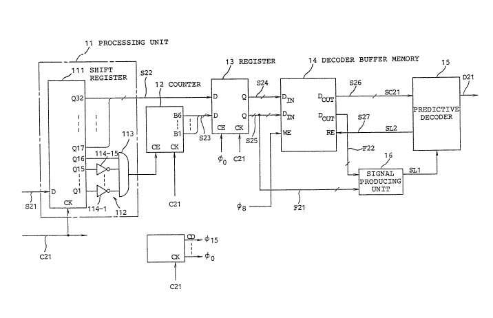
Referring now to Fig. 2, attention will be
directed to a predictive decoding device according to a
first embodiment of this invention. The predictive
10 decoding device is for use as a counterpart of tlle
conventional predictive encoding device described with
reference to Fig. 1 in decoding an encoded video signal
S21 produced by the predictive encoding device in bit
series. Responsive to the encoded video signal S21, the
15 predictive decoding device produce a decoded video
signal D21.
Referring to Fig. 3, brief description will be
again made as regards the conventional predictive
encoding device before description of the embodiment.
20 An input video signal Sll' is shown along a top line and
is encoded by the conventional predictive encoding
device by the use of a frame selection signal S12' shown
along a second line in the manner described in
conjunction with Fig. 1. The conventional predictive
2~ encoding device transmits transmission data comprising
encoded data at a constant bit rate through a
transmission line to the predictive decoding device
illustrated in Fig. 2. The predictive decoding device
35~
12
receives the transmission data as -the encoded video
signal S21 shown along a third line of Fig~ 3. In the
example being illustrated, the input video signal Sll'
and the frame selection signal S12' are identical with
5 the input video signal Sll and the frame selection
signal S12, respectively. In this connection, the
decoded video signal S21 is identical with the encoded
video signal S13 illustrated in Fig. 1.
Referring back to Fig. 2 and afresh to Fig. 4,
10 the predictive decoding device comprises a processing
unit 11, a counter 12, a register 13, a decoder buffer
memory 14, a predictive decoder 15, and a signal
producing unit 16. It may be mentioned here that the
predictive decoding device receives the video signal S21
15 at a bit rate or with a bit cycle of the transmission
line. The encoded video signal S21 is supplied to the
processing unit 11 in bit series in synchronism wikh a
clock C21 which is shown along a top line of Fig. 4 and
has the bit rate of the transmission line. The encoded
20 video signal S21 is shown along a second line of Fig. 4
and comprises encoded data of the respective frames and
frame head data at heads of the respective frames. The
encoded data comprises successive variable-length data
or successive constant-length data. Each of the
25 variable-length data and the constant-length data has a
data length which is not longer than sixteen bits. The
frame head datum FHD consists of sixteen bits which has
a bit pattern of fifteen O's and a single 1 following
3L'~6~3~5~
13
the O's. The frame head datum may be said to represent
a unique code.
The processing unit 11 comprises a shift
register 111 and a logic circuit 112. The shift
5 register 111 is of a 32-bit type having first through
sixteenth bit terminals Ql to Q16 and seventeenth
through thirty-second bit terminals Q17 to Q32 and is
for separating the bit serial encoded data of the
encoded video signal S21 into the frame head data and
10 the encoded data. The shift register 111 produces the
frame head data through the first through the sixteenth
bit terminals Ql to Q16 in bit parallel and the encoded
data through the seventeenth through the thirty-second
bit terminals Q17 to Q32 in bit parallel as a processed
15 video signal S22. The logic circuit 112 is for
detecting the frame head data and comprises an AND gate
113 which has first through sixteenth input terminals.
The first through the fifteenth input terminals of the
AND gate 113 are connected to the first through the
20 fifteenth bit terminals Ql to Q15 of the shift register
111 via first through fifteenth inverters 114-1 to
114-15, respectively. The sixteenth input terminal of
the AND gate 113 is directly connected to the sixteenth
bit terminal of the shift register 111. The AND gate
25 113 delivers a frame head pulse FHP to the counter 12 on
detection of the frame head data. The frame head pulse
FHP is shown along a third line of Fig. 4 and has a
S~
14
pulse width which is e~ual to single bi-t cycle of the
clock C21.
The counter 12 is supplied with the frame head
pulse FHP and the clock C21. The counter 12 is a mod-26
5 counter and is for counting pulses of the clock C21.
The frame head pulse F~P is delivered to a count enable
terminal CE of the counter 12 and makes the counter 12
count the pulses of the clock C21. The frame head pulse
FHP is therefore called a count enable signal. The
10 counter 12 produces count data as an original frame
number signal S23 each time when the frame head pulses
FHP appears. The original frame number signal S23
consists of first through sixth bit signals Bl to B6
which can represent 0 through 63. The original frame
15 number signal S23 is shown along a fourth line of Fig. 4
and represents the respective frame numbers of the
encoded video signal S21 in numerical order. Therefore,
the counter 12 may be called a number giving unit. It
is to be noted khat the maximum frame number represented
20 by the original frame number signal is not smaller than
the number of frames which can be stored in the decoder
buffer memory 14. For example, the frame numbers 10 and
11 are illustrated in Fig. 4. The count data of the
counter 12 are held until the counter 12 is supplied
2~ with the next frame head pulse FHP.
The predictive decoding device further comprises
an additional counter 17 which is a mod-24 counter. The
additional counter 17 counts the pulses of the clock C21
1268~
and produces count data CD comprising zeroth through
fifteenth bit signals ~0 to ~15 in bit parallel. The
count data CD cyclically increase from zero to fifteen
as shown along a fifth line of Fig. 4.
The processed video signal S22 and the original
frame number signal S23 are supplied to the register 13.
The register 13 is for writing the processed video
signal S22 and the original frame number signal S23 in
the decoder buffer memory 14 by aligning the processed
10 video signal S22 and the original frame number signal
S23 in the following manner. The register 13 is also
supplied with the clock C21 and the zeroth bit signal ~0
of the additional counter 17. The register 13 stores
the processed video signal S22 as first store data and
15 the original frame number signal S23 as second store
data in synchronism with the clock C21. In the register
13, the first and the second store data are
simultaneously cleared on reception of the zeroth bit
signal ~0. At this instant of time, the register 13
20 produces the first store data as a buffer input signal
S24 and the second store data as a second buffer input
signal S25. The first buffer input signal S24 is
represented by sixteen parallel bits and is supplied to
the decoder buffer memory 14 as a first part of write-in
25 data. The first buffer input signal S24 is shown along
a sixth line of Fig. ~ and is held by the zeroth bit
signal ~0 during sixteen bit cycles of the clock C21.
The second buffer input signal S25 is represented by six
12~8~S~
16
parallel bits and is divided into two parts, one of
which is supplied to the decoder buffer memory 14 as a
second part of the write-in da-ta. The other part is
supplied to -the signal producing unit 16 as a first
5 frame number signal F21 to carry out a comparing
operation as will be aescribed la-ter. The first frame
number signal F21 is shown along a fourth line of Fig. 3
and also shown along a seventh line of Fig. 4. The
first frame number signal F21 is held during a single
10 frame period.
The decoder buffer memory 14 temporarily stores
the first buffer input signal S24 as main data and the
second buffer input signal S25 as subdata each time when
a write enable terminal WE receives the eighth bit
15 signal ~8 of the additional counter 17. The eighth bit
signal ~8 i9 shown along a bottom line of Fig. 4 and may
be called a write enable signal. The decoder buffer
memory 14 is for carrying out speed conversion between a
write-in speed and a read-out speed, namely, a decoding
20 speed of the predictive decoder 15. Needless to say,
the read-out speed is faster than the write-in speed.
An FIFO ~first-in firs-t-out) memory is useful as the
decoder buffer memory 14. The decoder buffer memory 14
produces the main data as a read-out signal S26
25 represented by sixteen parallel bits and the subda-ta as
a second frame number signal F22 represented by six
parallel bits in response to a supply control signal S27
produced by the predictive decoder 15. The second frame
S~
17
number signal F22 is shown along a fifth line of Fig. 3.
The supply control signal S27 is shown along a sixth
line of Fig. 3 and is generated in the manner which will
be described later.
The read-out signal S26 is supplied to the
predictive decoder 15 as read-out data of the decoder
buffer memory 14 through a supplying circuit SC21 which
has sixteen lines. Namely, the supplying circuit SC21
is operable as a first supplying circuit. The second
10 frame number signal F22 is supplied to the signal
producing unit 16. The signal producing unit 16 may be
a comparator in the example being illustrated and is for
comparing the frame number represented by the first
frame number signal F21 and the frame number represented
15 by the second frame number signal F22. Needless to say,
the first frame number signal F21 represents the frame
number of the write-in data of the decoder buffer memory
14 while the second frame number siqnal F22 represents
the ~rame number of the read-out signal S26 of the
20 decoder buffer memory 1~. When the frame number of the
write-in data coincides with the frame number o~ the
read-out signal S26, it is necessary to suppress
production of the read-out signal S26 in order to
prevent underflow of the decoder buffer memcry 14.
The signal producing unit 16 produces a decoder
control signal only when the frame number of the
write~in data coincides with the frame number of the
read-out signal S26. The decoder control signal is
5~
18
supplied through a first control signal line SLl to the
predictive decoder 15. The first control signal line
SLl is operable as a second supplying circui-t. The
predictive decoder 15 detects presence or absence of the
5 decoder control signal at the beginning of each frame of
the read-out signal S26. The predictive decoder 15
stops production of read-out signal S26 during the next
following frame on detection of the decoder control
signal. On detection of the decoder control signal, the
10 predictive decoder 15 produces the supply control signal
S27 of a binary "0" value. The supply control signal
S27 is delivered back to the decoder buffer memory 14
through a second control signal line SL2. The second
control signal line SL2 is operable as a third supplying
15 circuit. The supply control signal S27 is for
controlling production of the read-out signal S26 and
has a binary "1" value when the signal producing unit 16
does not produce the decoder control signal. Namely,
the read-out signal S26 is delivered to the predictive
20 decoder 15 only when the supply control signal S27 has
the binary value "1." The supply control signal S27 of
the logic "1" value may be called a read enable signal.
Responsive to the read-out signal S26, the
predictive decoder 15 decodes the read-out signal S26,
25 namely, the encoded data, into the decoded video signal
D21 in the manner known in the art. In the absence of
the read-out signal S26, the predictive decoder 15 holds
the next previous ~rame of -the decoded video signal D21
~ ~B~
19
by using a frame memory which comprises in the manner
known in the art. The decoded video signal D21 is shown
along a seventh line of Fig. 3. Numerals shown along a
bottom line of Fig. 3 represent delays in the respective
5 frames of the decoded video signal D21 at the number of
the frames. The respective frames of the decoded video
signal D21 shown in Fig. 3 has variable delays which are
not longer than the constant delay described in
conjunction with Fig. 1.
Referring to Fig. 5, the description will
proceed to a predictive decoding device according to a
second embodiment of this invention. The predictive
decoding device deals with signals, some of which are
similar to those described in connection with Fig. 2.
1~ Other of the signals are different. More specifically,
the predictive decoding device is for use in processing
the encoded video signal S21 in bit seriesO At any
rate, the predictive decoding device carries out
decoding operation which is similar to that described in
20 conjunction with Fig. 2. Therefore, description will be
made briefly.
Besides similar parts designated bv like
reference numerals, the predictive decoding device
comprises a predictive decoder 15', a detecting unit 21,
25 a multiplexing unit 22, a separating unit 23, and a
signal producing unit 24. The predictive decoder 15' is
similar to that illustrated in Fig. 2 except that the
predictive decoder 15' produces a frame signal in the
35~
manner which will be described later. As described in
conjunction with Fig 4, the encoded video signal S21
comprises the encoded data of the respective frames and
the frame head data at heads of the respective frames.
5 The encoded video signal S21 is divided in-to two parts,
one of which is supplied to the detecting unit 21. The
other part is supplied to the multiplexing unit 22. The
detecting unit 21 i5 for detecting the frame head data
included in the encoded video signal S21. The detecting
10 unit 21 may comprise the logic circuit 112 described in
conjunction with Fig. 2. The detecting unit 21 produces
the frame head pulses on detection of the frame head
data. The frame head pulses are supplied to the counter
12. The counter 12, namely, the number giving unit,
15 produces the first frame number signal F21 each time
when the frame head pulse appears. The first frame
number signal F21 is supplied to the multiplexing unit
22 and the signal producing unit 24.
Responsive to the encoded video signal S21 and
2~ the first frame number signal F21, the multiplexing unit
22 multiplexes the encoded video signal S21 and the
first frame number signal F21 into a multiplexed signal.
More specifically, the multiplexing unit 22 inserts the
first frame number signal F21 between the frame head
25 data and the encoded data of the encoded video signal
S21. The multiplexed signal is supplied to the decoder
buffer memory 14 as write-in data. The decoder buffer
memory 14 temporarily stores the multiplexed signal. As
~2ti~3~35~
described with reference to Fig. 2, the decoder buffer
memory 14 produces read-out data in response to the
supply control signal S27 produced by the predictive
decoder 15'. The read-out data are supplied to the
5 separating unit 24. Responsive to the read-out da-ta,
the separating unit 23 separates the read-out data into
a separated first frame number signal and separated
encoded data. The separating unit 23 produces -the
separated first frame number signal as the second frame
10 number signal F22 and the separated encoded data as the
read-out signal S26. The separating unit 23 is operable
as a first signal producing circuit. The second frame
number signal F22 represents the frame numbers indicated
by the first frame number signal F21 and is supplied to
15 the signal producing unit 24. The read-out signal S26
is supplied through a supplying circuit SC22 to the
predictive decoder 15'. The supplying circuit SC22 is
operable as a first supplying circuit.
Responsive to the read-out signal S26, the
20 predictive decoder 15' produces the frame signal at each
head of the frames. The signal producing unit 24
compares the frame number represented by the first frame
number signal F21 with the frame number represented by
the second frame number signal F22 in response to the
25 frame signal. The frame signal is used in timing the
first and the second frame number signals F21 and F22.
The signal producing unit 24 produces the decoder
control signal only when the frame number repxesent~d by
22
the first frame number signal F21 coincides with the
frame number represented by the second frame number
signal F22. The decoder control signal is supplied
through the first control signal line SLl to the
5 predictive decoder 15'. The first control signal line
SLl is operable as a second supplying circuit.
The predictive decoder 15' produces the frame
signal at the beginning of each frame of -the read-out
signal S26. The frame signal is supplied through a
10 timing signal line TLl to the signal producing unit 24.
Besides, the predictive decoder 15' produces the supply
control signal S27 with the binary "0" value in the
presence of the decoder control signal to stop
production of the read-out data of the next following
15 rame. On the other hand, the predictive decoder 15'
produces the supply control signal S27 with the binary
"1" value on the absence of the decoder control signal
to read out the read-out data. The supply control
signal S27 is delivered through the second control
20 signal line SL2 back to the decoder buffer memory 14.
The second control si~nal line SL2 is operable as a
third supplying circuit. Thus, the decoder buffer
memory 14 produces the read-out data when the supply
control signal S27 has the binary "1" value and stops
25 the production of the read-out data of the next
following frame when the supply control signal S27 has
the binary "0" value~
1.~ 5~
23
Responsive to the read out signal S26, the
predictive decoder 15' decodes the read out signal S26
into the decoded video signal D21. In the absence of
the read-out signal S26, the predictive decoder 15'
5 holds the next previous frame of the decoded video
signal D21.
Referxing to Fig. 6, the description will
further proceed to a predictive decoding device
according to a third embodiment o this invention. The
10 predictive decoding device is for use as a counterpart
of a predictive encoding device comprising the detecting
unit, the counter, and the multiplexing unit described
with r~eference to Fig. 5. In this event, the predictive
encoding device transmits a multiplexed signal into
15 which frame number data and encoded data are
multiplexed.
The predictive decoding device deals with
signals, most of which are similar to those described in
conjunction with Fig. 5~ The predictive decoding device
20 carries out decoding operation which is similar to that
described with reference to Fig. 5.
Besides similar parts designated by like
reference numerals, the predictive decoding device
comprises an additional signal producing unit 31. The
25 predictive decoding device receives the multiplexed
signal as an encoded video signal depicted in Fig. 6 at
S21'. The encoded video signal S21' comprises encoded
data of a sequence of frames given successive frame
1;~68~
24
numbers and frame number data indicative o~ the
respective frame numbers. The encoded video signal S21'
is supplied to the decoder buffer memory 14 as write-in
data and is supplied to the additional signal producing
5 unit 31. Responsive to the encoded video signal S21',
the additional signal producing unit 31 produces the
first frame number signal F21 by detecting the frame
number data multiplexed in the encoded video signal
S21'. The first frame number signal F21 represents the
10 frame numbers indicated by the respective frame number
data of the encoded video signal S21', namely, the
write-in data. The additional signal producing unit 31
is operable as a first signal producing circuit. The
first frame number signal F21 is supplied to the signal
15 producing unit 24.
Responsive to the encoded video signal S21', the
decoder buffer memory 14 stores the encoded video siynal
S21'. The decoder bu~fer memory 14 produces read-out
data in response to the supply control signal S27 in the
20 manner described in conjunction with Fig. 5. The
read-out data are supplied to the separating unit 23.
Responsive to the read-out data, the separating unit 23
separates the read-out data into the frame number data
and the encoded data. The separating unit 23 delivers
25 separated frame number data as the second frame number
signal F22 to the signal producing unit 24 and delivers
separated encoded data as the read-out signal S26
through the supplying circuit SC22 to the predictive
. - ..
`"` ~Z~:~8~
decoder 15'. The separating unit 23 is operable as a
second signal producing circuit. The suppl~ing circuit
SC22 is opera~le as a first supplying circuit. The
second frame number signal F22 represents the frame
5 numbers indicated by the frame number data included in
the read-out data.
As described with reference to Fig. 5, the
predictive decoder 15' produces the frame signal at the
beginning of each ~rame of the read-out signal S26. The
10 frame signal is supplied through the timing signal line
TLl to the signal producing unit 24. On reception of
the frame signal, the signal producing unit 2~ compares
the frame nun~er represented by the first frame number
signal F21 with the frame number represented by the
15 second frame number signal F22. The signal producing
unit 24 produces the decoder control signal in the
manner described in conjunction with Fig. 5. The signal
producing unit 24 is operable as a third signal
producing circuit. The decoder control signal is
20 supplied throùgh the first control signal line SLl to
the predictive decoder 15'. The first control signal
line SLl is operable as a second supplying circuit.
The predictive decoder 15' produces the supply
control signal S27 with the binary "0" value in the
25 presence of the decoder control signal and produces the
supply control signal with the binary "1" value in the
absence of the decoder control signal. The supply
control signal S27 is delivered through the second
5~
26
control signal line SL2 back to the decoder bufEer
memory 14. The second control signal line SL2 is
operable as a third supplying circuit. The decoder
buffer memory 14 produces the read-out data when the
5 supply control signal S27 has the binary "1" value and
stops ~he production of the read-out data of the next
following frame when the supply control signal S27 has
the binary "0" value.
Responsive to the read-out signal S26, the
10 predictive decoder 15' decodes the read-out signal S26,
namely, the encoded data, into the decoded video signal
D21. In the absence of the second separated signal, the
predictive decoder holds the next previous frame of the
decoded video signal D21.
While this invention has thus far been described
in conjunction with a few preferred embodiments thereof,
it will readily be possible for those skilled in the art
to put this invention into practice in various other
manners. For example, the predictive decoding device
20 may be either an in-frame decoding devicé and an
interframe decoding device. Incidentally, it will be
understood that compression encoding is carried out on
the input video signal on a frame basis. More
particularly, the compression encoding is achieved by
25 frame thinning or subsampling and additionally by
in-frame and interframe encoding.