Language selection

Search

Patent 1268873 Summary

Third-party information liability

Some of the information on this Web page has been provided by external sources. The Government of Canada is not responsible for the accuracy, reliability or currency of the information supplied by external sources. Users wishing to rely upon this information should consult directly with the source of the information. Content provided by external sources is not subject to official languages, privacy and accessibility requirements.

Claims and Abstract availability

Any discrepancies in the text and image of the Claims and Abstract are due to differing posting times. Text of the Claims and Abstract are posted:

  • At the time the application is open to public inspection;
  • At the time of issue of the patent (grant).
(12) Patent: (11) CA 1268873
(21) Application Number: 547488
(54) English Title: LINE INTERFACE CIRCUIT
(54) French Title: CIRCUIT D'INTERFACE POUR LIGNE DE COMMUNICATION
Status: Deemed expired
Bibliographic Data
(52) Canadian Patent Classification (CPC):
  • 379/63
(51) International Patent Classification (IPC):
  • H04Q 1/28 (2006.01)
  • H04M 19/00 (2006.01)
(72) Inventors :
  • MOISIN, MIHAIL STEFAN AUGUSTIN TRAIAN (Canada)
(73) Owners :
  • NORTEL NETWORKS LIMITED (Canada)
(71) Applicants :
(74) Agent: MOORHOUSE, J. E.
(74) Associate agent:
(45) Issued: 1990-05-08
(22) Filed Date: 1987-09-22
Availability of licence: N/A
(25) Language of filing: English

Patent Cooperation Treaty (PCT): No

(30) Application Priority Data: None

Abstracts

English Abstract


LINE INTERFACE CIRCUIT
Abstract of the Disclosure
A line interface circuit supplies energizing
current for operation of a two wire communication line and
couples a.c. signals between the communication line and a
telephone facility. Tip and ring rails are resistively
connected to the communication line by matched feed resistors
in a resistance network also including tip and ring taps.
Active impedance circuits in an a.c. signal coupling circuit
terminate the tip and ring rails with a predetermined
impedance, via the feed resistors, in response to voltages at
the tip and ring taps. Active resistance valving circuits in
a direct current feed circuit supply the communication line
with energizing direct current via the tip and ring rails and
feed resistors. The valving circuits may be controlled to
limit current for shorter lines and the functions of the a.c.
signals coupling circuit may be optimally altered in response
thereto. In one example, operating band width is extended
into ISDN frequencies by providing a secondary resistance
network with secondary feed resistors coupling secondary tip
and ring rails to the tip and ring rails. In this structure,
the a.c. signal coupling circuit is responsive to a.c.
signals at secondary tip and ring taps for terminating the
secondary rails and a supervisory circuit is responsive to
the voltages at the tip and ring taps for generating
supervisory signals for the telephone facility.


Claims

Note: Claims are shown in the official language in which they were submitted.


23
THE EMBODIMENTS OF THE INVENTION IN WHICH AN EXCLUSIVE
PROPERTY OR PRIVILEGE IS CLAIMED ARE DEFINED AS FOLLOWS:-
1. A line circuit for interfacing tip and ring
leads of a telephone line with a telephone facility,
comprising:
tip and ring terminals for connection to the tip
and ring leads;
an a.c. signal feed termination, including active
impedance tip and ring means, for coupling substantially only
alternating current signals between the tip and ring
terminals and the telephone facility;
a direct current feed termination, including active
resistance tip and ring means, for valving substantially only
direct current via the tip and ring terminals;
a resistance network including, a tip feed resistor
connected to the tip terminal and each of the active tip
means, a ring feed resistor connected to the ring terminal
and each of the active ring means, and tip and ring voltage
dividers having tip and ring voltage taps each being
connected to an input of the a.c. signals feed termination.

2. A line circuit for interfacing tip and ring
leads of a telephone line with a telephone facility,
comprising:
a direct current feed termination for valving
substantially only direct current via the telephone line;
a primary resistance network including primary tip
and ring feed resistors for connection between tip and ring
leads of the telephone line and the direct current feed
termination;
an a.c. signal feed termination for coupling
substantially only alternating current signals between the
telephone line and the telephone facility;
a secondary resistance network including secondary
tip and ring feed resistors being connected between the a.c.
signal feed termination and respective ones of the primary tip
and ring feed resistors, and the secondary resistance network
further including secondary tip and ring voltage dividers


24
having tip and ring taps being connected to a differential
input of the a.c. signal feed termination;
whereby in operation the primary tip and ring feed
resistors carry all of the current traversing the telephone
line while the secondary tip and ring feed resistors are
limited to a.c. current components traversing the telephone
line to the exclusion of direct current.

3. A line interface circuit, for interfacing a
telephone line and a telephone facility, comprising:
tip and ring terminals for connection to tip and
ring leads of the telephone line;
a direct current feed termination, including active
resistance tip and ring means, for valving energizing direct
current via the telephone line tip and ring terminals, and a
current limiting means whereby the energizing direct current
is restrained from exceeding a predetermined limit;
an a.c. signal feed termination including active
impedance tip and ring means, for coupling a.c. signals
between the tip and ring terminals and the telephone
facility, an equalization means being responsive to a
restraint of the energizing direct current for varying gain
and impedance characteristics of the a.c. signal feed
termination accordingly; and
a resistance network including, a tip feed resistor
connected between the tip terminal and each of the active tip
means, a ring feed resistor connected between the ring
terminal and each of the active ring means, and tip and ring
voltage dividers having tip and ring voltage taps connected
to an input of the a.c. signals feed termination.

4. A line interface circuit comprising:
a direct current feed termination for valving
energizing direct current via a telephone line and including
a current limiting means whereby the energizing direct
current is restrained from exceeding a predetermined limit;
a primary resistance network including primary tip
and ring feed resistors for connection between tip and ring


leads of the telephone line and the direct current feed
termination;
an a.c. signal feed termination for coupling a.c.
signals between the telephone line and a telephone facility,
the a.c. signal feed termination including an equalization
means being responsive to a restraint of the energizing
direct current for varying gain and impedance
characteristics of the a.c. signal feed termination
accordingly;
a secondary resistance network including secondary
tip and ring feed resistors being connected between the a.c.
signal feed termination and respective ones of the primary
tip and ring feed resistors, and the secondary resistance
network further including secondary tip and ring voltage
dividers having tip and ring taps being connected to a
differential input of the a.c. signal feed termination;
whereby in operation the primary tip and ring feed
resistors carry all of the current traversing the telephone
line while the secondary tip and ring feed resistors are
limited to a.c. current components traversing the telephone
line to the exclusion of direct current.

5. A line interface circuit, for terminating a two
wire communication line and for coupling a.c. signals between
the communication line and a hybrid circuit, the line
interface circuit comprising:
tip and ring terminals for connection to the
communication line;
ground and battery terminals for connection to a
source of energizing power;
tip and ring rails;
a resistance network including tip and ring feed
resistors being connected between the tip and ring terminals
and the respective tip and ring rails, and tip and ring taps
within tip and ring voltage dividers;
a differential amplifier circuit including inputs
connected to the tip and ring taps, and an output,;


26
an a.c. feedback path connected between the output
and an inverting input of the differential amplifier circuit;
tip and ring amplifiers each having an input and an
output;
a transformer including tip and ring primary
windings and a secondary winding, the tip primary winding
being connected between the tip rail and the output of the
tip amplifier, the ring primary winding being connected
between the ring rail and the output of the ring amplifier,
and the secondary winding being for connection to the hybrid
circuit;
a coupling network for coupling a.c. signals from
the output of the differential amplifier circuit to the input
of one of the tip and ring amplifiers and for coupling an
inverted replica of said a.c. signals to the input of the
other of the tip and ring amplifiers;
tip and ring direct current valving means for
conducting energizing direct current between the ground and
power terminals and the respective tip and ring rails, while
substantially excluding conduction of currents in association
with any differential a.c. voltages appearing on the tip and
ring rails; and
d.c. control means for restricting conductance of
current flow through the tip and ring direct current valving
means.

6. A method for interfacing a two wire
communication line and a telecommunication facility
comprising:
providing a resistance network including tip and
ring feed resistors and tip and ring taps on tip and ring
voltage dividers;
valving energizing direct current, to the
substantial exclusion of differential alternating currents,
through the communication line via a valving means and the
tip and ring feed resistors;
coupling signal representation of signals appearing


27
at the tip and ring taps to the telecommunications facility;
and
feeding the communications line differentially in
antiphase in response to substantially only differential a.c.
signals appearing at the tip and ring taps and feeding the
communication line differentially in response to a.c. signals
from the telecommunications facility via a feed means,
whereby the communications line is terminated with an a.c.
impedance being substantially independent of a resistance
associated with the valving of the energizing direct current.

7. A method for interfacing a two wire
communication line and a telecommunications facility
comprising:
providing primary and secondary resistance
networks, each including tip and ring feed resistors and tip
and ring taps in tip and ring voltage dividers, the tip feed
resistors being connected in series and the ring feed
resistors being connected in series respectively;
valving energizing direct current through the
communication line via a resistive feed means and the tip and
ring feed resistors of the primary resistance network;
coupling signal representation of signals appearing
at the tip and ring taps of the secondary resistance network
to the telecommunications facility, and
in response to differential a.c. signals appearing
at the tip and ring taps of the secondary resistance network
and a.c. signals from the telecommunication facility, feeding
the communication line differentially in antiphase with
respect to said appearing a.c. signals, whereby the
communication line is terminated with an a.c. impedance being
substantially independent of a resistance associated with the
feeding of the direct energizing current.

8. A method as defined in claim 6 where in an
instance of said communication line being of less than a
predetermined resistance to a flow of the energizing direct
current:


28
the resistance associated with the valving of the
direct energizing current is increased to effect an upper
limit of the energizing current flow; and
the differential feeding of the communication line
is varied to become simultaneously more responsive to the
a.c. signals appearing at the tip and ring taps and less
responsive to the a.c. signals from the telecommunications
facility, the variation progressing in relation to the amount
of increase of said resistance associated with the valving of
the energizing direct current.

9. A method as defined in claim 7, where in an
instance of said communication line being of less than a
predetermined resistance to a flow of the energizing direct
current:
the resistance associated with the valving of the
direct energizing current is increased to effect an upper
limit of the energizing current flow; and
the differential feeding of the communication line
is varied to become simultaneously more responsive to the
a.c. signals appearing at the tip and ring taps and less
responsive to the a.c. signals from the telecommunications
facility, the variation progressing in relation to the amount
of increase of said resistance associated with the valving of
the energizing direct current.

10. A line interface circuit for supplying
energizing current for operation of a two wire communication
line and for coupling a.c. signals between the communications
line and a telephone facility, comprising:
tip and ring terminals for connection to the
communications line;
ground and battery terminals for connection to a
source of energizing direct current;
tip and ring rails;
a resistance network including tip and ring feed
resistors being connected between the tip and ring terminals
and the tip and ring rails respectively, a tip voltage


29
divider being connected between the tip rail and the ring
terminal and including a tip tap, and a ring voltage divider
being connected between the ring rail and the tip terminal
and including a ring tap;
a.c. signals coupling means including tip and ring
active impedance feed means being connected to the tip and
ring rails respectively, a differential amplifier circuit
having inputs connected to the tip and ring taps and having
an output for providing a.c. signals, in response to
differential signals on the communication line, for operation
of the tip and ring active impedance feed means, the a.c.
signals coupling means, each having an output being operable
for coupling a.c. signals between the communication line and
the telephone facility;
a direct current feed means including, tip and ring
active resistance valving means for conducting energizing
direct currents between the ground and power terminals and
the tip and ring rails, wherein one of said valving means is
operative to conduct at a predetermined resistance and the
other of said valving means is operative to conduct at a
resistance which maintains a voltage difference across said
other valving means similar to a voltage difference across
said one valving means.

11. A line interface circuit as defined in claim
10, wherein the direct current feed means further includes:
a rail tap means for providing a rail tap voltage
about midway between voltages at the tip and ring rails;
a power tap means for providing a power tap voltage
about midway between voltages at the ground and power
terminals;
control means being responsive to the rail and
power tap voltages for generating a current control signal to
which said other valving means is responsive for regulating
said voltage difference.

12. A line interface circuit as defined in claim
10, wherein the direct current feed means further includes:


a current limit control circuit for generating a
current limit signal to which said one active resistance
valving means is responsive for increasing said resistance to
be greater than said predetermined resistance, in an event
wherein said energizing current corresponds to a
predetermined limit.

13. A line interface circuit as defined in claim
10, wherein the direct current feed means further includes:
a rail tap means for providing a rail tap voltage
about midway between voltages at the tip and ring rails;
a power tap means for providing a power tap voltage
about midway between voltages at the ground and power
terminals;
control means being responsive to the rail and
power tap voltages for generating a current control signal to
which said other valving means is responsive for regulating
said voltage difference; and
a current limit control circuit for generating a
current limit signal to which said one valving means is
responsive for increasing said resistance to be greater than
said predetermined resistance, in an event wherein said
energizing current corresponds to a predetermined limit.

14. A line interface circuit for supplying
energizing current for operation of a two wire communication
line and for coupline a.c. signals between the communications
line and a telephone facility, comprising:
tip and ring terminals for connection to the
communications line;
ground and battery terminals for connection to a
source of energizing direct current;
tip and ring rails;
a resistance network including tip and ring feed
resistors being connected between the tip and ring terminals
and the tip and ring rails respectively, a tip voltage
divider being connected between the tip rail and the ring
terminal and including a tip tap, and a ring voltage divider


31
being connected between the ring rail and the tip terminal
and including a ring tap;
a.c. signals coupling means including tip and ring
active impedance feed means being connected to the tip and
ring rails respectively, a differential amplifier circuit
having inputs connected to the tip and ring taps and having
an output for providing a.c. signals, in response to
differential signals on the communication line, for
operation of the tip and ring active impedance feed means,
the a.c. signals coupling means being operable for coupling
a.c. signals between the communications line and the
telephone facility;
a direct current feed means including, tip and ring
active resistance valving means for conducting energizing
direct currents between the ground and power terminals and
the tip and ring rails, wherein one of said valving means is
operative to conduct at a predetermined resistance and the
other of said valving means is operative to conduct at a
resistance which maintains a voltage difference across said
other valving means similar to a voltage difference across
said one valving means;
and each of the tip and ring active resistance
valving means comprising:
a current feed resistor being connected to a
respective one of the power and ground terminals;
a voltage follower circuit including an input and a
transistor having an emitter electrode connected to the
current feed resistor and a collector electrode connected to
a respective one of the tip and ring rails;
a direct current voltage divider including
resistive elements being connected between said respective
terminal and rail and defining first and second voltage taps,
the first voltage tap being resistively closer to the
terminal than the second voltage tap, the input of the
voltage follower circuit being connected to the first voltage
tap, resistance values of the resistance elements in the
direct current voltage divider being such that the transistor
is normally operated near a saturation mode of operation;


32
one of the tip and ring active resistance valving
means further comprising;
a current limit control circuit being connected to
the first voltage tap and including a non linear conductive
device for limiting a voltage difference between said
terminal and the first voltage tap whereby the transistor may
be operated in a mode substantially remote from said
saturation mode of operation; and
the other of the tip and ring active resistance
valving means further comprising:
a rail voltage divider being connected between the
tip and ring rails and including a rail tap;
a power voltage divider being connected between the
ground and power terminals and including a power tap;
a differential amplifier having inputs connected
across the rail and power taps and an output connected to the
second voltage tap of the direct current voltage divider, for
causing said other active resistance valving means to mimic
operation of said one active resistance valving means.

15. A line interface circuit as defined in claim
10, wherein the a.c. signals coupling means further
comprises:
a transformer including,
a tip primary winding being connected between the
tip rail and a junction associated with the output of the tip
active impedance feed means,
a ring primary winding being connected between the
ring rail and a junction associated with the output of the
ring active impedance feed means, and
a secondary winding for connection to the telephone
facility:
a coupling network for coupling a.c. signals from
the output of the differential amplifier circuit to the tip
active impedance feed means, for coupling an inverted replica
of the a.c. signals to the ring active impedance feed means,
and including a reactive network for defining a nominal
effective impedance at each of said junctions; and


33
wherein the tip active impedance feed means
includes a differential amplifier having an inverting input
and an output connected to said junction, and a non-inverting
input being connected to the coupling network for receiving
said a.c. signals; and
wherein the ring active impedance feed means
includes a differential amplifier having an inverting input
and an output connected to said junction, and a non-inverting
input being connected to the coupling network for receiving
said replica signals.

16. A line interface circuit as defined in claim
15, further comprising an equalization circuit means within
the coupling network, the equalization circuit means being
responsive to a current limiting occurrence in one of the
direct current feed means for modifying a function of the
coupling network.

17. A line interface circuit as defined in claim
15, wherein the direct current feed means further includes:
a rail tap means for providing a rail tap voltage
about midway between voltages at the tip and ring rails;
a power tap means for providing a power tap voltage
about midway between voltages at the ground and power
terminals;
control means being responsive to the rail and
power tap voltages for generating a current control signal to
which said other valving means is responsive for regulating
said voltage difference.

18. A line interface circuit as defined in claim
15, wherein the direct current feed means further includes:
a current limit control circuit for generating a
current limit signal to which said one active resistance
valving means is responsive for increasing said resistance to
be greater than said predetermined resistance, in an event
wherein said energizing current corresponds to a
predetermined limit.


34
19. A line interface circuit as defined in claim
15, wherein the direct current feed means further includes:
a rail tap means for providing a rail tap voltage
about midway between voltages at the tip and ring rails;
a power tap means for providing a power tap voltage
about midway between voltages at the ground and power
terminals;
control means being responsive to the rail and
power tap voltages for generating a current control signal to
which said other valving means is responsive for regulating
said voltage difference; and
a current limit control circuit for generating a
current limit signal to which said one valving means is
responsive for increasing said resistance to be greater than
said predetermined resistance, in an event wherein said
energizing current corresponds to a predetermined limit.

20. A line interface circuit as defined in claim
15, wherein the tip and ring active resistance valving means
each comprises:
a current feed resistor being connected to a
respective one of the power and ground terminals;
a voltage follower circuit including an input and a
transistor having an emitter electrode connected to the
current feed resistor and a collector electrode connected to
a respective one of the tip and ring rails;
a direct current voltage divider including
resistive elements being connected between said respective
terminal and rail and defining first and second voltage taps,
the first voltage tap being resistively closer to the
terminal than the second voltage tap, the input of the
voltage follower circuit being connected to the first voltage
tap, resistance values of the resistance elements in the
direct current voltage divider being such that the transistor
is normally operated near a saturation mode of operation: and
wherein one of the tip and ring active resistance
valving means further comprises;


a current limit control circuit being connected to
the first voltage tap and including a non linear conductive
device for limiting a voltage difference between said
terminal and the first voltage tap whereby the transistor may
be operated in a mode substantially remote from said
saturation mode of operation; and
wherein the other of the tip and ring active
resistance valving means further comprises:
a rail voltage divider being connected between the
tip and ring rails and including a rail tap;
a power voltage divider being connected between the
ground and power terminals and including a power tap;
a differential amplifier having inputs connected
across the rail and power taps and an output connected to the
second voltage tap of the direct current voltage divider, for
causing said other active resistance valving means to mimic
operation of said one active resistance valving means.

21. A line interface circuit as defined in claim
20, further comprising an equalization circuit, for changing
the effective operating impedance at said junction in
response to active current limiting of the energizing
current.

22. A line interface circuit as defined in claim
20, further comprising an equalization circuit, within the
coupling network, for changing the effective operating
attenuation at said junction in response to active current
limiting of the energizing current.

23. A line interface circuit for terminating a two
wire communication line and for coupling a.c. signals between
the communication line and a telephone facility, the line
interface circuit comprising:
tip and ring terminals for connection to the
communication line;
ground and battery terminals for connection to a
source of energizing power


36
primary tip and ring rails;
a primary resistance network including primary tip
and ring feed resistors being connected between the tip and
ring terminals and the primary tip and ring rails
respectively, and primary tip and ring taps within primary
tip and ring voltage dividers;
a primary differential amplifier circuit including
inputs connecting the primary tip and ring taps, and an
output, the primary differential amplifier circuit being
responsive to potentials appearing at the primary tip and
ring taps for generating supervisory signals for use in the
telephone facility;
a direct current feed means including, tip and ring
active resistance valving means for conducting energizing
direct currents between the ground and power terminals and
the primary tip and ring rails, wherein one of said valving
means is operative to conduct at a predetermined resistance
and the other of said valving means is operative to conduct
at a resistance which maintains a voltage difference across
said other valving means similar to a voltage difference
across said one valving means;
secondary tip and ring rails;
a secondary resistance network including secondary
tip and ring feed resistors being connected between the
respective secondary tip and ring rails and the primary tip
and ring rails, and secondary tip and ring taps within
secondary tip and ring voltage dividers; and
a.c. signals coupling means including tip and ring
active impedance feed means being connected to the secondary
tip and ring rails respectively, a differential amplifier
circuit having inputs connected to the secondary tip and ring
taps and having an output for providing a.c. signals, in
response to differential signals on the communication line,
for operation of the tip and ring active impedance feed
means, the a.c. signals coupling means being operable for
coupling a.c. signals between the communication line and the
telephone facility.


37
24. A line interface circuit as defined in claim
23, wherein the direct current feed means further includes:
a primary rail tap means for providing a rail tap
voltage about midway between voltages at the primary tip and
ring rails;
a power tap means for providing a power tap voltage
about midway between voltages at the ground and power
terminals;
control means being responsive to the rail and
power tap voltages for generating a current control signal to
which said other valving means is responsive for regulating
said voltage difference.

25. A line interface circuit as defined in claim
23, wherein the direct current feed means further includes:
a current limit control circuit for generating a
current limit signal to which said one active resistance
valving means is responsive for increasing said resistance to
be greater than said predetermined resistance, in an event
wherein said energizing current corresponds to a
predetermined limit.

26. A line interface circuit as defined in claim
23, wherein the direct current feed means further includes:
a primary rail tap means for providing a rail tap
voltage about midway between voltages at the primary tip and
ring rails;
a power tap means for providing a power tap voltage
about midway between voltages at the ground and power
terminals;
control means being responsive to the rail and
power tap voltages for generating a current control signal to
which said other valving means is responsive for regulating
said voltage difference; and
a current limit control circuit for generating a
current limit signal to which said one valving means is
responsive for increasing said resistance to be greater than


38
said predetermined resistance, in an event wherein said
energizing current corresponds to a predetermined limit.

27. A line interface circuit as defined in claim
23, wherein each one of the tip and ring active resistance
valving means comprises:
a current feed resistor being connected to a
respective one of the power and ground terminals;
a voltage follower circuit including an input and a
transistor having an emitter electrode connected to the
current feed resistor and a collector electrode connected to
a respective one of the primary tip and ring rails;
a direct current voltage divider including
resistive elements being connected between said respective
terminal and rail and defining first and second voltage taps,
the first voltage tap being resistively closer to the
terminal than the second voltage tap, the input of the
voltage follower circuit being connected to the first voltage
tap, resistance values of the resistance elements in the
direct current voltage divider being such that the transistor
is normally operated near a saturation mode of operation; and
wherein one of the tip and ring active resistance
valving means further comprises;
a current limit control circuit being connected to
the first voltage tap and including a non linear conductive
device for limiting a voltage difference between said
terminal and the first voltage tap whereby the transistor may
be operated in a mode substantially remote from said
saturation mode of operation; and
wherein the other of the tip and ring active
resistance valving means further comprises:
a rail voltage divider being connected between the
primary tip and ring rails and including a rail tap;
a power voltage divider being connected between the
ground and power terminals and including a power tap;
a differential amplifier having inputs connected
across the rail and power taps and an output connected to the
second voltage tap of the direct current voltage divider, for


39
causing said other active resistance valving means to mimic
operation of said one active resistance valving means.

28. A line interface circuit as defined in claim
3, wherein the equalization circuit comprises:
a receive lead for receiving a.c. signals from the
telephone facility;
a transmit lead for transmitting a.c. signals to
the telephone facility;
amplifier means being responsive to any a.c.
receive signals on the receive lead and any differentially
sensed line signals for generating a transmit signal on the
transmit lead;
ring and tip drive amplifiers being responsive to
the transmit signal for generating non-inverted and inverted
signals for driving tip and ring amplifiers; and
variable attenuation means being responsive to a
restraint of the energizing direct current for altering
response of the tip and ring drive amplifiers whereby an
effective a.c. terminating impedance of the line interface
circuit is adjusted.

29. A line interface circuit as defined in claim
28, wherein the variable attenuator means also reduces
response of the amplifying means to the differentially sensed
line signals, to the exclusion of the a.c. receive signals,
in response to restraint of the energizing direct current.

30. A line interface circuit as defined in claim
4, wherein the equalization circuit comprises:
a receive lead for receiving a.c. signals from the
telephone facility;
a transmit lead for transmitting a.c. signals to
the telephone facility;
amplifier means being responsive to any a.c.
receive signals on the receive lead and any differentially
sensed line signals for generating a transmit signal on the
transmit lead;


ring and tip drive amplifiers being responsive to
the transmit signal for generating non-inverted and inverted
signals for driving tip and ring amplifiers; and
variable attenuation means being responsive to a
restraint of the energizing direct current for altering
response of the tip and ring drive amplifiers whereby an
effective a.c. terminating impedance of the line interface
circuit is adjusted at outputs of the tip and ring
amplifiers.

31. A line interface circuit as defined in claim
30, wherein the variable attenuator means also reduces
response of the amplifying means to the differentially sensed
line signals, to the exclusion of the a.c. receive signals,
in response to restraint of the energizing direct current.

32. A line interface circuit as defined in claim
28, further comprising:
an amplifier for coupling said differentially
sensed line signals with either of at least two selectable
gain factors whereby the line interface circuit is adapted to
receive said line signals from a communication line of either
of more than one predetermined characteristic impedance.

33. A line interface circuit as defined in claim
29, further comprising:
an amplifier for coupling said differentially
sensed line signals with either of at least two selectable
gain factors whereby the line interface circuit is adapted to
receive said line signals from a communication line of either
of more than one predetermined characteristic impedance.

34. A line interface circuit as defined in claim
28, further comprising:
switch means for selecting an operating gain of
said tip and ring drive amplifiers whereby more than one
predetermined effective terminating impedance is selectable
for terminating the communication line.


41
35. A line interface circuit as defined in claim
29, further comprising:
switch means for selecting an operating gain of
said tip and ring drive amplifiers whereby more than one
predetermined effective terminating impedance is selectable
for terminating the communication line.

36. A line interface circuit for coupling a.c.
signals between a communication line and an associated
telephony facility, including;
tip and ring amplifiers being operable for
terminating the communication line with a predetermined
impedance in response to differential alternating currents in
the communication line, and a current limiting device being
operable to limit energizing direct current flow in the
communication line in an instance wherein said flow would
otherwise exceed a predetermined limit, the line interface
circuit being characterized by:
an equalization circuit, being responsive to an
instance of said current limiting for modifying said response
to said differential alternating currents whereby the
terminating impedance is varied from said predetermined
impedance.

37. A line interface circuit as defined in claim
36, wherein the equalization circuit includes means for
increasing alternating current antiphase drive of the
communication line via the tip and ring amplifiers during
said instance of current limiting.

38. A method for terminating tip and ring leads of
a two-wire communication line comprising the steps of:
a) providing a resistance network including tip and
ring resistors being connecting in series between the tip and
ring rails, and including tip and ring taps in tip and ring
voltage dividers;


42
b) valving energizing direct current flows, to
exclude differential alternating current, via a battery
supply, valving means, the tip and ring rails, resistors and
the tip and ring leads; and
c) actively terminating the tip and ring rails with
an impedance being less than a characteristic impedance of
the communication line by an amount corresponding to a sum of
the ohmic values of the tip and ring resistors, via a feed
means, in response to differential voltages developed at the
tip and ring taps in response to differential currents in the
tip and ring resistors.

39. A method for terminating first and second
leads of a two-wire communication line comprising the steps
of:
a) providing a primary resistance network including
primary tip and ring resistors being connected in series
between the first and second leads and primary tip and ring
rails, and including primary tip and ring taps in primary tip
and ring voltage dividers;
b) providing a secondary resistance network
including secondary tip and ring resistors being connected in
series between the primary tip and ring rails and secondary
tip and ring rails, and including secondary tip and ring taps
in secondary tip and ring voltage dividers;
c) valving energized direct current flows, to
exclusion of differential alternating current, via the
primary tip and ring rails and resistors and the first and
second leads; and
d) actively terminating the secondary tip and ring
rails with an impedance being less than a characteristic
impedance of the communication line by an amount
corresponding to a sum of the ohmic values of the primary and
secondary tip and ring resistors, in response to differential
voltages developed at the secondary tip and ring taps in
response to differential currents in the secondary tip and
ring resistors.


43
40. A method as defined in claim 38, further
comprising the step of:
e) varying the valving of the energizing direct
current flows in proportion to a longitudinal signal on the
communication line, whereby corresponding longitudinal
voltage on the tip and ring rails is reduced.

41. A method as defined in claim 39, further
comprising the step of:
f) varying the valving of the energizing direct
current flows in proportion to a longitudinal signal on the
communication line, whereby corresponding longitudinal
voltage on the primary tip and ring rails is reduced.

42. A line interface circuit for terminating a two
wire communication line and for coupling a.c. signals between
the communication line and a hybrid circuit, the line
interface circuit comprising:
tip and ring terminals for connection to the
communication line;
ground and battery terminals for connection to a
source of energizing power;
primary tip and ring rails;
a primary resistance network including tip and ring
feed resistors being connected between the tip and ring
terminals and the respective primary tip and ring rails, and
primary tip and ring taps within primary tip and ring voltage
dividers;
a primary differential amplifier circuit including
inputs connecting the primary tip and ring taps, and an
output, the primary differential amplifier circuit being
responsive to potentials appearing at the primary tip and
ring taps for generating supervisory signals;
tip and ring direct current valving means for
conducting energizing direct current between the ground and
power terminals and the respective primary tip and ring
rails, while substantially excluding conduction of currents


44
in association with any differential a.c. voltages appearing
on the primary tip and ring rails;
d.c. control means for restricting conductance of
current flows through the tip and ring valving means;
secondary tip and ring rails;
a secondary resistance network including secondary
tip and ring feed resistors being connected between the
respective secondary tip and ring rails and the primary tip
and ring rails, and secondary tip and ring taps within
secondary tip and ring voltage dividers;
a secondary differential amplifier circuit
including inputs connected to the secondary tip and ring
taps, a feedback network having a.c. and d.c. feedback paths,
one of said inputs being for connection to the hybrid circuit
and an output for connection to the hybrid circuit;
tip and ring amplifiers each having an input and an
output, the output being connected to a respective one of the
secondary tip or ring rails; and
a coupling network for coupling a.c. signals from
the output of the secondary differential amplifier to the
input of one of the tip and ring amplifiers and for coupling
an inverted replica of said a.c. signals to the input of the
other tip and ring amplifier.

43. A line interface circuit as defined in claim
42, wherein the output of the tip amplifier is resistively
connected to the secondary tip rail and an inverting input of
the tip amplifier, and wherein the output of the ring
amplifier is resistively connected to the secondary ring rail
and an inverting input of the ring amplifier.


Description

Note: Descriptions are shown in the official language in which they were submitted.


1~68~t73

LINE INTERFACE CIRCUIT
The invention is in the field of telephony
communication line interface circuits and more particularly
concerns a line circuit wherein alternating current signal
components and direct current components are interfaced via
respective active impedance and active resistance circuits.
Background of the Invention
In recent years, various line interface circuits
have been developed wherein the tip and ring leads of a
subscriber's loop are terminated directly or indirectly at
tip and ring active feed means, as exemplified in each of the
following listed United States patents:
4,321,430 - Ferrieu (March 23, 1982)
4,387,273 - Chea, Jr. (June 7, 1983)
4,484,032 - Rosenbaum (November 20, 1984)
4,514,595 - Rosenbaum et al (April 30, 1985)
4,539,438 - Rosenbaum et al (September 3, 1985)
4,571,460 - Rosenbaum et al (February 1~, 1986)
In the later four listed patents, examples of line
circuits described therein usually include a.c. and d.c.
feedback networks or the like which serve to determine the
effective operating output impedances of the active feed
means.
It is an object of the invention to provide a line
interface circuit wherein a.c. line impedance termination and
d.c. line feed resistance termination are segregated and
independent one from the other.
In each of the four examples, a non-linear element
may be combined with the d.c. feedback network whereby line
feed current is limited to a predetermined value by
increasing the resistances of the active feed means. This
feature is useful for conservation of current supply on short
subscriber loops, however it may be deleterious to voice
quality as it effectively inhibits the equalization
characteristics of a typical telephone set remotely connected
to the short communication line. In the designs of typical
telephone sets, response characteristics of both the
transmitting and receiving apparatus therein have been
taylored to compensate for the lesser signal loss on short

8~7~3


loops. The transmitting and receiving apparatus are arranged
to be progressively less sensitive in the presence of line
current in excess of about 40 milliamps. Therefore, in short
loops a function of line current limiting increases a.c.
signal levels, received from the typical telephone, to beyond
that normally expected in the telephone system.
Another problem in termination of telephone lines
is that the typical line interface circuit is adaptable to
one of only two specified standard impedances. One being
specified for the majority of telephone lines and the other
being specified for extremely long telephone lines which are
inductively loaded to enhance analog voice band transmission.
In actual practice however, not all telephone lines are of
one or the other standard impedance, and hence in full duplex
operation the hybrid circuit function is less th2n optimal
and may permit oscillation sometimes referred to as singing
because of insufficient return loss. Operating telephone
companies usually avoid this problem by a simple expedient of
having about eight decibels of loss in each line interface
circuit. Hence in a typical telephone conversation between
telephone subscribers, about sixteen decibels of loss is
inserted between the transmitter of one subscriber and the
receiver of another subscriber. Recently, some telephony
networking features of private branch exchanges in
combination with one or more operating companies involve four
or more two-wire communication lines and line interface
circuits in a tandem connectionO In such an arrangement,
typically more than forty decibels of loss is inserted,
making conversation difficult in all but the ~uietest of
environments.
It is an object of the invention to obtain an
effective measure of the communication line from a current
limiting action in the d.c. line feed resistance termination,
and to use this measure to vary the a.c. line impedance
termination accordingly whereby attenuation and return loss
values, in a group of typical telephone lines, are more
consistently optimized.
One structural characteristic common to many of the


examples in the previously mentioned patents is that of a
resistance network which includes tip and ring feed resistors
arranged in series between tip and ring leads of the
communication line and tip and ring active impedance feed means.
The resistance network also includes tip and ring voltayes
dividers including tip and ring taps from whence d.c. voltages
are utilized for detection of supervisory states and a.c.
voltages are utilized to receive voice band information and to
dynamically control the tip and ring active impedance feed means.
As a practical matter, it is preferred that the resistance
network be provided on a supporting substrate and that individual
resistive elements be trimable to achieve close ohmic matches
between various of the resistors. If the line interface circuit
is to be adapted for higher than voice band frequency signals, as
for example may be the case of terminating a "U" interface in an
integrated subscriber digital network (ISDN), parasitic
capacitances associated with the physical resistance elements
must also be closely matched. Any reactive mismatch, for
example a picofarad or so, is amplified by following amplifier
elements, such as to render the line circuit virtually useless at
ISDN operating frequencies. Unfortunately, precision matching of
the parasitic capacitance to the degree required is at least for
the present impractical.
It is therefore an object of the invention to provide a
line interface circuit having a practical operating band width of
about 200 KHz which includes the audio spectrum and the ISDN 2B-~D
basic rate service U interface band width requirements.

Summar~ of the Invention
A line interface circuit, in accordance with the
invention, comprises a direct current feed termination for
providing energizing current for operation of a two wire
communication line, and an a.c. signal feed termination for
coupling a.c. signals between the communication line and a
telecommunications facility. The feed terminations are
connected in parallel to tip and ring feed resistors for
connection to tip and ring leads of the communication line.

;8~3~3


The tip and ring feed resistors are part of a resistance
network which includes tip and ring voltage taps in tip and
ring voltage dividers, the tip and ring voltage taps being
connected to a differential input of the a.c. signal feed
termination.
A method for interfacing a two wire communication
line and a telecommunication facility, in accordance with the
invention, comprises providing a resistance network including
tip and ring feed resistors and tip and ring taps in tip and
ring voltage dividers. Energizing direct current is valved
through the communications line via the tip and ring feed
resistors. Signal representation of signals appearing at the
tip and ring taps are coupled to the telecommunications
facility. In response to differential a.c. signals appearing
at the tip and ring taps and a.c. signals from the
telecommunications facility, alternating current is fed,
differentially in antiphase with respect to the a.c. signals
at the tip and ring taps, to the communication line.
Thereby, the communication line is terminated with an a.c.
impedance being substantially independent of a resistance
associated with the valving of the energizing direct current.
In one example, a line interface circuit includes
tip and ring terminals for connection to a communication line
and ground and battery terminals for connection to a source
of energizing direct current. A resistance network includes
tip and ring feed resistors which are connected between the
tip and ring terminals and tip and ring rails respectively.
The resistance network also includes tip and ring voltage
dividers having respective tip and ring taps. An alternating
current coupling means includes tip and ring active impedance
feed means heing connected to the tip and ring rails
respectively, and a differential amplifier circuit with
inputs connected to the tip and ring taps. The active
impedance feed means are responsive to a.c. signals from the
output of the differential amplifier circuit for terminating
the communication line with a prede-termined a.c. impedance
such that the a.c. coupling means is operative for coupling
a.c. signals between the communication line and a -telephone

1268~3


facility. The line interface circuit also includes a direct
current feed means including tip and ring active resistance
valving means for conducting energizing direct currents
between the ground and power terminals and the tip and ring
rails. One of the valving means is operative to conduct at a
predetermined resistance and the other of the valving means
is operative to conduct at a resistance which maintains a
voltage difference across the other valving means which is
similar to a voltage difference across the one valving means.
In another example, the line interface circuit
includes a transformer with tip and ring primary windings,
each being connected in series between the tip and ring rails
and the respective tip and ring active impedance feed means,
and a coupling network. The coupling network is operative
for coupling a.c. signals and an inversion of same to inputs
of the respective tip and ring active impedance feed means.
The coupling network also includes a reactive network for
defining nominal effective operating feed impedances of the
feed means. The line circuit may also include an
equalization circuit being responsive to a current limiting
occurrence in one of the feed means for modifying a function
of the coupling network to improve a return loss operating
characteristic of a hybrid circuit associated with the
communication line.
Yet another example of a line interface circuit, in
accordance with the invention, includes tip and ring
terminals for connection to a communication line and ground
and battery ter~inals for connection to a source of power. A
primary resistance network includes primary tip and ring feed
resistors being connected between the tip and ring terminals
and primary tip and ring rails respectively, and primary tip
and ring taps within primary tip and ring voltage dividers.
A primary differential amplifier circuit includes inputs
connected to the primary tip and ring taps and is responsive
to voltages at these taps for generating supervisory signals
for use in a telephone facility. A direct current feed
circuit includes tip and ring active resistance valving means
for conducting energizing direct currents between the ground

B~3


and power terminals and the primary tip and ring ralls. A
secondary resistance network includes secondary tip and ring
feed resistors being connected between the primary tip and
ring rails and secondary tip and ring rails respectively, and
secondary tip and ring taps within secondary tip and ring
voltage dividers. An alternating current coupling means
includes tip and ring active impedance feed means being
connected to the secondary tip and ring rails respectively,
and a differential amplifier circuit with inputs connected to
the secondary tip and ring taps. The active impedance feed
means is responsive to a.c. signals from the output of the
differential amplifier circuit for terminating the
communication line with a predetermined impedance such that
the a.c. coupling means is operable for coupling a.c. signals
between the communication line and the telephone facility.
Brief Description of the Drawings
Example embodiments are discussed with reference to
the accompanying drawings in which:-
Figure 1 is a block schematic diagram of a line
interface circuit in accordance with the invention;
Figure 2 is a schematic diagram illustrating onedetailed example of the line interface circuit in Figure 1;
Figure 3 is a block schematic diagram illustrating
a line interface circuit as in Figures 1 or 2 with the
addition of a line transformer;
Figure 4 is a block schematic diagram of another
line interface circuit, in accordance with the invention;
Figure 5 is a block schematic diagram showing some
exemplary details of the line interface circuit illustrated
in Figure 4;
Figure 6 is a block schematic diagram of another
example of the line circuit shown in Figure 4;
Figure 7 is a schematic diagram illustrating one
example of an equalization circuit used in the line interface
circuit in Figure 6; and
Figure 8 is a block schematic diagram of another
example of a line circuit including a line interface
transformer somewhat similar to that shown in Figure 3, and

73

which includes an equalization circuit as for example is
illustrated in Figure 7.
Description of the Example Embodiments
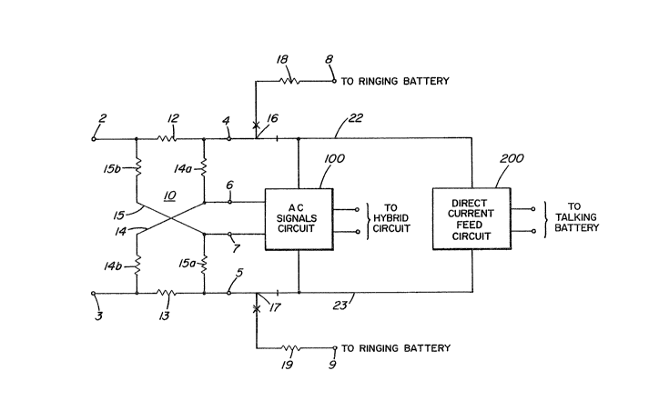
The line circuit illustrated in Figure 1 includes a
resistance network 10 which is connected between tip and ring
terminals 2 and 3 and tip and ring rails 22 and 23 via tip
and ring rail terminals 4 and 5. An a.c. signal circuit 100
and a direct current feed circuit 200 are each connected in
parallel one with the other to the tip and ring rail
terminals 4 and 5 via the tip and ring rails 22 and 23.
Alternately, relay transfer contacts 16 and 17 may be
operated to connect ringing battery (not shown) by way of
ringing battery terminals 8 and 9 and ringing battexy feed
resistors 18 and 19 to the tip and ring rail terminals 4 and
5, to the exclusion of the tip and ring rails 22 and 23.
Furthermore, protection devices or networks, not
shown, are typically connected to the tip and ring rail
terminals 4 and 5 and/or rails 22 and 23 and sometimes in
association with the tip and ring terminals 2 and 3. Such
devices are intended to divert itinerant current spikes
and/or surges away from the circuits 100 and 200, and so
preserve the operational integrity of these circuiks.
However, as this function and the function of the ringing
current feed via the resistors 18 and 19 are not of direct
interest regarding the invention, these elements of a typical
telephone line interface circuit are not further discussed.
The direct current feed circuit 200 is connected to
a source of power, usually a 50 volt battery or the like, in
an associated telephone facility, not shownO The source of
power is typically referred to as a talking battery. The
direct current feed circuit 200 functions by providing a
resistively regulated active feed path between the talking
battery and tip and ring feed resistors 12 and 13 in the
resistance network 10, and thence to an OFF HOOK subscriber
telephone line. The feed circuit 200 at the same time
operates with an impedance suf~icient to block differential
alternating currents. The telephone line is not shown but is
normally connected to the tip and ring terminals 2 and 3O Of

~ t7~


course, the subscriber line is in an ON HOOK condition, when
the line is open and hence substantially no current should be
drawn from the talking battery.
The resistance network 10 includes tip and ring
voltage dividers 14 and 15 which are provided by resistors
l~a and 14b and 15a and 15b connected as shown to provide tip
and ring taps 6 and 7. In normal operation, the a.c. signals
circuit 100 is responsive to differential signals at the tip
and ring taps 6 and 7 to drive the tip and ring rails 22 and
23 in antiphase thereto, to reduce these voltages at the
terminals 2 and 3 as if the telephone line were terminated at
some impedance. The amount of the impedance is determined by
an internal impedance network, the actual impedance of which
is determined in accordance with the desired terminating
impedance for the telephone line and by the response
characteristics of circuits within the a.c. signal circuit
100. The circuit 100 also receives a.c. signals from a
hybrid circuit, not shown, in the associated telephone
facility and transmits these via the tip and ring rails, and
in addition, provides the hybrid circuit within signals
preferably to the exclusion of longitudinal signals as these
signals appear at the tip and ring taps 6 and 7. These
functions of direct current feed and impedance termination
are advantageously provided by the separate circuits 100 and
200 in that variations or adjustments may be affected with
respect to one of these functions with little or no
consequence to the other of these functions.
One detailed example of circuitry suitable for
providing the line interface circuit of Figure 1 is
illustrated in Figure 2. In Figure 2 and in the subsequent
figures, elements which are the same are identified by the
same labels. In the case of circuit blocks having a label
including a units digit 0, there may be some minor variations
between one figure and another. Where such circuit blocks
are discussed, such variations are likewise discussed. Only
those power and ground paths as may be helpful in the
understanding of the structure and function of the
illustrated example are shown, in the interests of brevity


:,. ~.. ..


and simplicity of description.
Referring specifically to Figure 2, the resistance
network 10 is connected to a detector circuit 150 which is
provided by a differential amplifier 151 and associated
resistor elements 152 to 154 connected as shown. In
operation, the output 158 of the differential amplifier 151
provides ON HOOK and OFF HOOK indications and a.c. signals
corresponding to differential a.c. signals appearing at the
tip and ring taps 6 and 7. Immunity to longitudinal signals
as may be introduced along the communication line is
dependent not only upon the common mode rejection
characteristiGs of the differential amplifier 151 but also on
the precision matching of ohmic values of the tip and rlng
feed resistors 12 and 13 and also upon the precision matching
of ohmic values of the tip and ring voltage divider resistors
14a and 14b and 15a and 15b.
An a.c. signals coupling network 160 is connected
between the output 158 and tip and ring active impedance feed
circuits 130 and 140. The function of the network 160 is to
couple a.c. driving signals of one phase to the tip circuit
130 and of an opposite phase to the ring circuit 140. The
network 160 also includes an impedance network placed between
the output 158 and a lead 155 for defining the response of
the differential amplifier 151 to a.c. signals, thereby
defining the effective terminating impedance of the tip and
ring circuits 130 and 140.
Fach of the tip and ring active impedance feed
circuits 130 and 140 is provided by a differential amplifier
131 and 141 arranged in one of two optionally configured
voltage follower configurations. For example, the output of
the amplifier 131 is either connected directly via a path 132
to a junction 134 of its inverting input and tip rail 22, or
connected indirectly via a resistor 133 to a junction 134.
Likewise a corresponding arrangement prevails in the ring
active impedance feed circuit 140. When the resistance
option is used, 100 Ohm resistors 133 and 143, for e~ample,
permit test observations of amplifier functions without
consequence to the function of the operating line circuit.

~L2~ 73


The direct current feed circuit 200 as used in any
of the figures is illustrated in detail in Figure 2 and
includes ring and tip active resistance valving circuits 210
and 220, and a follower control circuit 230. The direct
current feed circuit 200 also includes a direct coupled
control means 240, which functions to provide a feed current
limit control and overvoltage protection.
The ring active resistance valving circuit 210
includes an amplifier 211 connected in a voltage follower
configuration with an NPN transistor 212 being connected in
series with a resistor 213 between a negative potential -V
terminal of the talking battery and the ring rail 23. A
voltage divider includes resistors 215, 216 and 217 connected
between the -V terminal and the ring rail 23 and provides
15 voltage taps 216a and 219, as shown. A capacitor 218 is
connected between -V terminal and the voltage tap 219 to
provide an a.c. ground at the voltage tap 219. A resistor
214 is connected be~ween the voltage tap 216a and a non-
inverting input of the amplifier 211. The tip active
resistance valving circuit 220 includes similar circuit
elements connected in a similar configuration between the
ground terminal of the talking battery and the tip rail 22,
however in this case, the transistor 222 is a PNP device.
The following control circuit 230 includes a differential
amplifier 231 having a non-inverting input connected to a
rail tap at a junction of resistors 232 and 233 which are
connected in series between the tip and ring rails 22 and 23.
The inverting input of the differential amplifier 231 is
connected to a power tap at a junction of resistors 234 and
235 which are connected in series between the ground and the
-V terminal. An output of the differential amplifier 231 is
resistively coupled to the voltage tap 229 by a resistor 236.
In normal function as thus far introduced, the tip
and ring active resistance valving circuits 220 and 210
operate under the control of the respective voltage dividers
such that when the subscriber line is in the OFF HOOK
condition, part of the resistance to direct current flow ls
provided by the transistors 212 and 222, with mo~t of the

~26~73


remainder of the resistance being provided by the tip and
ring feed resistors 12 and 13. For example, in an
arrangement requiring a 400 Ohm feed resistance, the tip and
ring feed resistors would each be 100 Ohms, the resistor 213
and 223 would each be about 20 Ohms and an active resistance
of about 80 Ohms would be imparted by the valving action of
each of the transistors 212 and 222. Under these conditions,
the amount of direct energizing current flow is substantially
determined by the length of the subscriber line. The
presence of the follower control circuit 230 is not normally
of any consequence under these conditions. In this example
however, the follower contxol circuit also includes a
capacitive coupling via capacitors 237 and 238 and junctions
237a and 238a, to the non-inverting inputs of the amplifiers
221 and 211. By this arrangement, the tip and ring active
resistance valving circuits present virtually no active
resistance, only passive resistance to longitudinal currents
as may be induced on the subscriber line to which the line
interface circuit is connected. By means of negative
feedback, this circuit implements in fact two common mode
virtual grounds for longitudinal a.c. currents, over the tip
and ring rails 22 and 23 and therefore two low impedance
paths for longitudinal a.c. currents.
By deleting capacitors 237 and 238, alternative low
impedance paths are achieved for longitudinal currents via
resistors 135 and 145 to the junctions 134 and 144 which are
two common mode virtual grounds. Matching requirements apply
for the resistors 135 and 145 in this case, in order to meet
the longitudinal balance re~uired performance. This is an
optional arrangement ~hich is particularly advantageous in
the example line interface circuit illustrated in Figures 4
to 7. However this description is introduced in Figure 2 as
a matter of illustrative convenience.
The feed current limit control circuit 240 includes
an NPN transistor 241 having an emitter electrode connected
to the -V terminal and a collector electrode connected to the
tap 216a of the voltage divider 215 to 217 such that any
significant potential at a base electrode of the transistor

~ ~6~ 3


12
241 causes a potential at the tap 216a to be drawn toward the
-V terminal potential. By selection of appropriate
resistance values for resistors 245 and 242 it is arranged
that at about 40 milliamperes of current flow in the resistor
213, about half a volt or so lesser negative voltage than the
potential of the -v terminal appears at the junction of these
resistors. This causes the transistor 241 to conduct a
little which increases the negative voltage at the junction
216a. Consequently, the current flow via the transistor 212
is restricted, causing the voltage on the ring rail 23 to be
reduced toward ground. Sufficient voltage reduction on the
ring rail 23 as might be caused by a ground fault somewhere
along the ring side of the subscriber loop, will cause a 24
volt Zener diode 243 to conduct via a resistor 244. This has
an effect of turning on the transistor 241 and valving the
transistor 212 to be almost off. Normally, the feed current
limit control circuit only operates with any effect when a
short and hence low resistance loop is connected across the
tip and ring terminals 2 and 3. In this event as before
mentioned, current is partially restricted or valv~d at the
transistor 212. A resulting voltage shift at the ring rail
23 is sensed by the following control circuit 230, which in
turn causes a complementary valving action in the transistor
222 and a complementary shift of voltage at the tip rail 22.
This use of current limiting introduces an a.c.
terminating problem. In any poplllation of subscriber loops,
the majority of the loops are of moderate to long length and
thus each exhibits a charac~eristic impedance very close to
that preferred and specified, for example in Local Area
Telecommunications Authority Switching System General
Requirements (L.S.S.G.R.) published by Bellcore. Such loops
do not activate the current limiting function. However in
actual practice the shorter loops, are normally concentrated
in heavily populated urban centres and normally draw more
than 40 milliamps of current. Such loops are each in actual
fact of a lower than specified characteristic impedance.
Over the years, this problem has been partially compensated
by operating characteristics of many telephone station sets

~6~7~
13
wherein thermistors are used to attenuate received signals
and a carbon microphone of lesser efficiency at high
energizing currents is also used. At the line interface
circuit, trans-hybrid loss in any two-wire four-wire
conversion function is reduced by mismatch. That is to say
that the side tone becomes greater than that attained with
the proper impedance match. In order to prevent
oscillations, sometimes referred to as singing, which may
occur under some operating conditions, it is a typical
practice of an operating telephone company to use a hybrid
circuit, usually of the electronic type, which introduces
about eight to ten decibels of bidirectional attenuation in
addition to the typical hybrid function. This has proven to
be quite acceptable for typical telephone usage. However, in
a telephone call invoking special PBX features, which may
require a conversation to traverse at least four line
interface circuits, accumulated loss can become intolerable.
It is an object of the invention to provide an equalizing
function within the line interface circuit whereby signal
levels are reduced only on shorter loops, independently of a
hybrid circuit, and in accordance with a feed current
limiting function in the line interface circuit.
In Figure 2, the functions of differential signal
response and common mode rejection are very dependent on a
very high standard of operation of the differential amplifier
151. These functions are optimized by obtaining the closest
possible match of the tip and ring feed resistors 12 and 13
and similar tolerance of match between the resistors 14a and
14b and 15a and 15b. However, because the direct current
feed function is separate from the a.c. signal termination
function as shown in figures 1 and 2, voice band a.c. signal
termination and feed functions are enhanced, without
requiring any impractical matching of resistance values in
the network 1~, by utilization of a line circuit transformer
as is exemplified in Figure 3. The line interface circuit in
Figure 3 is substantially the same as that illustrated in
Figure 2, except that a very small line circuit transformer
30 is introduced. Being very small, such transformers are

8~7;~

1~
cheap to manufacture or purchase and are easily mounted on a
printed circuit board. In this case, the transformer may be
very small as it is completely isolated from any direct
current. As shown, the transformer includes tip and ring
primary windings 32 and 33 connected between the junction 13~
and the tip rail 22 and the junction 144 and the ring rail 23
respectively. A secondary winding 31 is shunted by a
resistor 34 which modifies the apparent low frequency
characteristics of the transformer 30. The secondary winding
is connectable to a hybrid circuit in the associated
telephone facility via terminals 36 in this case, since the
primary windings 32 and 33 are very well matched by
construction and since the d.c. resistance of the primary
windings 32 and 33 is very low, it is preferable to delete
15 capacitors 237 and 238 from the circuit 200 and thus to
implement the longitudinal current paths via the primary
windings 32 and 33 to the common mode virtual grounds at the
junctions 134 and 144.
Another recent problem realized in the technolo~y
of line interface circuits is that of extending the operatin~
frequency of such circuits through the ISDN basic rate
frequency band, that is to at least 200 kilohertz. It has
been found that in circuits which rely upon tip and ring taps
for sensing line signals that even very close matching of
resistances in the resistance network 10 is insufficient to
extend the desired operating bandwidth to more than about
twice the typical telephone voice band. The apparent reason
for this problem is that of parasitic capacitance mismatch
among the resistance elements in the network 10. One
solution to this problem is to both reduce and match the
parasitic capacitance however, at this time this solution
appears to be virtually impossible to practice. Another
solution which tolerates parasitic capacitance is that of a
line interface circuit design as exemplified in Figure 4.
Figure ~ is similar to the preceding figures in
that it includes the a.c. signal circuit 100, the direct
current feed circuit 200 and the network 10, however in this
case the network 10 is now referred to as a primary

~.2G1~7;3

resistance network 10 as there is also introduced a secondary
resistance network 110. The networks are connected as shown
with a supervision circuit 300 and the a.c. signal circuit
100 respectively.
In operation, the supervision circuit 300 detects
ON HOOK and OFF HOOK states by sensing voltages developed by
current flows in the primary tip and ring feed resistors 12
and 13. The direct current feed circuit 200 operates
similarly as discussed in relation to the preceding figures
to feed energizing current via the tip and ring rails 22 and
23, the transfer contacts 16 and 17, the tip and ring rail
terminals 4 and 5, the tip and ring primary feed resistors 12
and 13, and the tip and ring terminals 2 and 3, to a
communication line (not shown) connected thereto. The a.c.
signal circuit 100 operates similarly as discussed in
relation to the preceding figures to provide a predetermined
impedance termination for coupling a.c. signals between the
communication line and a hybrid circuit in an associated
telephone facility (not shown). The secondary resistance
network 110 is similar to the primary resistance network 10
and has similar elements labeled similarly with a distinction
being that of a hundreds digit. Secondary tip and ring feed
resistors 112 and 113 are connected as shown between the
primary tip and ring rails 22 and 23 and secondary tip and
ring rails 122 and 123 respectively, via terminals 102 to
105. Secondary tip and ring taps 106 and 107 are connected
to the a.c. signal circuit 100. In operation, voltages at
the secondary tip and ring taps 106 and 107 are developed in
response to a.c. currents in the secondary tip and ring feed
resistors. By means of the primary and secondary networks
and the as~ociated circuitry, the operating frequency range
is significantly extended far beyond the analog voice band.
This is achieved because of the particular architecture of
the circuit. Since the circuit 200 implements two common
mode virtual grounds for longitudinal currents over the tip
and ring rails 22 and 23 as previously discussed, there are
not longitudinal currents flowing through resistors 112 and
113. Hence, the parasitic capacitances over either the


16
primary or secondary resistor networks 10 and 110 do not have
any negative impact on the longitudinal balance performance of
the circuit. Therefore capacitance matching is not a critical
requirement for operation at the higher frequencies.
one implementation of the line interface circuit in
Figure 4 is shown more detail in Figure 5. The structure and
operation of Figure 5 is generally self-evident in view of the
previous discussions. However, a few areas of the figures are
here discussed for clarity. The supervision circuit 300,
primarily consists of the detector circuit 150, discussed in
relation to figure 2, with the exception that the output 158 is
for connection solely to a supervision circuit in an associated
telephone facility. The a.c. signals circuit 100 is provided by
a differential amplifier circuit at 160 which includes an
15 amplifier 161 with an output 168 and a d.c. feedback path
including a resistor 164 and an a.c. feedback path including a
capacitor 169b and a resistor 169a connected as shown. A
resistor 167 is connected between one of the terminals 36 and an
inverting input of the amplifier 161 for receiving signals from
the hybrid circuit. The output 168 is for direct coupling to a
hybrid circuit via another of the terminals 36, and is also
connected to drive the tip active impedance feed circuit 130 via
a junction 139 and a capacitor 136. The ring active impedance
feed circuit 140 is driven at 149 by an inverter 168a and a
capacitor 146.
The line interface circuit illustrated in Figure 6 is
similax to that shown in Figure 5 but for the inclusion of an
equalization circuit 170. The equalization circuit 170 includes
receive and transmit leads for connection to the hybrid circuit
30 instead of the circuit 160. The output 168 is used by the
equalization circuit 170 to generate a transmit output signal
with a degree of gain as determined by an impedance control
signal which may be manually set, or software generated in the
telephone facility. The tip and ring circuits 130 and~140 are
driven to greater or lesser extent in anti-phase with the signals
at the secondary taps 107 and 106 in accordance with there being
one of some or no current limiting function as would be evidenced
by a potential at the junction 229. The tip and ring active

12~38~3
17
impedance feed circuits 130 and 140 are also driven via the
equalization circuit by signals received from the telephone
facility.
The equalization circuit is illustrated with
greater detail in Figure 7. In Figure 7, those elements with
identifying labels 190 to 198 provide for a variable gain
function in the equalization circuit. A circuit option shown
at 199 is useful to adapt the e~ualization circuit to the
example illustrated in Figure 8, as will be discussed. This
variable gain function is essential to the operation of the
equalization circuitO In contrast those elements with
identifying labels of 172 to 175 and 187c and 187d provide
for a switchable gain function which is merely convenient for
adapting a line interface circuit to one of two predetermined
or specified communication line characteristic impedances.
Hence these elements may be omitted from the equalization
circuit. In operation, the equalization circuit receives
a.c. signals via a capacitor 171 from the output 168 of the
differential amplifier circuit 160 (Figure 6). Corresponding
a.c. signals are applied at a junction of resistors 177 and
178 and are coupled via these resistors to inverting inputs
of amplifiers 180 and 190 respectively. Signals on a receive
lead from the hybrid circuit in the associated telephone
facility7 are also coupled to the inverting input of the
25 amplifier 180 via a resistor 178. An output of the amplifier
180 is connected to a transmit lead for supplying signals to
the hybrid circuit in the associated telephone ~acility.
This output is also connected to an input of an amplifier 187
via a resistor 184. The amplifier 187 functions as a voltage
follower to drive the ring active impedance feed circuit 140
via the lead 149 (Figure 6), and to drive an inverting
amplifier 189 via a resistor 188. An output of the amplifier
189 in turn is connected to drive the tip active impedance
feed circuit 130 via the lead 139 (Figure 6).
Indication of feed current limiting action in the
feed current limit control circuit 240 is relayed via the
follower control circuit 230, as previously discussed in
relation to Figure 2. This indication is received from the

7~


18
junction 229 and filtered to reduce any a.c. signal components
by a resistor 193b and a capacitor 1~3c. Also a.c. signal
components as might otherwise be coupled via a resistor 193a
are reduced. A junction of the components 193a, 193b and 193c
is connected to an input of an amplifier 193. Circuit
components at 194 are arranged to apply a predetermined
fraction of the -V terminal potential at an inverting input of
the amplifier 193, such that in the event of current limiting
the amplifler 193 responds by biasing a FET 195 ON in
proportion to a degree of the current limiting. The amplifier
193 drives the d.c. resistance of the FET to such a value to
maintain the d.c. voltage at the positive input of the
amplifier 193 equal to the constant d.c. voltage at the
negative input of the amplifier 193. On the other hand, the
value of the FET resistance controls the amount of signal
diverted to the amplifiers 180 and 182 via capacitor 197 and
resistors 198 and 185, which finally implement the equalization
feature.
As a conclusion, the live equalization is a direct,
continuous and deterministic function of the loop length.
This has an effect of proportionally coupling an inversion of
the a.c. signals received by the amplifier 190, via a resistor
192, and the FET 195 to a capacitor 196c and a resistor 196r,
connected as shown, and through a coupling capacitor 197.
Hence a.c. signals in antiphase are summed via a resistor 198
at the inverting input of the amplifier 180 to effectively
attenuate that portion of the transmit signal on the transmit
lead which was originally received on the lead 168. This
reduction does not have any effect on that portion of the
signal on the transmit lead which is coupled via the resistor
178 from the receive lead. These signals coupled via the
capacitor 197 are also applied to an input of an inverting
amplifier 182 via resistor 185. The output of the amplifier is
resistively coupled via resistor 186 to the junction of the
resistor 184 and the amplifier 187. Depending upon a ratio of
the ohmic values of the resistors 184 and 186, the ultimate
effect of a current limiting occurrence is arranged to modify
the antiphase a.c. feeding of the communication line by the tip

19
and ring circuits 130 and 140 to a predetermined degree, as
is desired.
Switches 174d and 187d are each arranged with
associated resistors 173c and 187c to reduce the gains of the
respective amplifiers 173 and 187 such that the line
interface circuit is controllable via an impedance control
lead 175, to provide an optimal termination for a
communications line of a lower characteristic impedance. In
this example, the component values tabled at the end of the
discussion provide for a 900 Ohm impedance while invoking of
the impedance option by the lead 175 provides for a 600 Ohm
impedance.
The line interface circuit illustrated in Figure 8
is similar to that illustrated in Figure 6 but for
replacement of the secondary resistance netwoxk 110 by a line
interface transformer for example the transformer 30,
previously discussed. Referring to Figures 8 and 7 together,
the RECEIVE lead in Figure 7 is driven by signals from a
hybrid circuit in the associated telephone facility via an
amplifier 37 (Figure 8) which also drives the primary winding
31 via resistors 34a and 34b. Hence these siynals are
inductively coupled to the tip and ring rails 22 and 23 via
the secondary windings 32 and 33. Signals from the tip and
ring rails 22 and 23 are likewise inductively coupled across
the transformer 30 and appear as voltage across the resistor
34b along with the signals form the hybrid circuit. These
signal voltages across the resistor 34b are coupled to the
hybrid circuit via an amplifier 38. Therefore in the
equalization circuit in Figure 7 the TRANSMIT lead is not
connected. The circuit at 199 in Figure 7 is connected to
the output of the amplifier 182 such that a.c. signals are
supplied to the junctions 237a and 238a in the tip and ring
active resistance valving circuits 210 and 220, respectively.
Numerous variations of the example embodiments will
become apparent to those of typical skill in the electronic
circuit design field with reference to the foregoing
discussion and the illustrations. The equalization circuit
may be applied to various prior art line interface circuits

~6~ 3


for example as hereinbefore referred to. Of course, it
should be understood that in any configuration, the
equalization circuit is in every instance responsive to a
current limiting function of the line interface circuit which
terminates a shorter communication line such that response to
differentially detected a.c. line signals is varied to
compensate for telephone station set operation induced by the
otherwise desirable current limiting function. Again, one of
the benefits derived is that of requiring less attenuation in
the service connection of a station set, attenuation which is
otherwise required to ensure protection from singing due to
less than ideal hybrid circuit performance.
Another advantage is that those subscriber lines
provided with a line interface circuit having an equalization
circuit will accommodate station set designs which may be
more economical in view of the lesser range of energizing
current operating requirements.
One of the components so far not previously
mentioned is resistor 178a shown in figure 7 as being
optionally connectable between the receive lead and the lnput
of the amplifier 190. The resistor is of no advantaye other
than that of altering the response of the egualization
circuit somewhat deleteriously so that the line interface is
limited in function to meet the present L.S.S.G.R. standard
specification. In the operation of the equalization circuit,
the inclusion of this resistor also causes reduction of those
signal components from the receive lead and which thus appear
on the transmit lead. Therefor this option is deleterious to
operation of an associated hybrid circuit.
Resistance values matched to within 1% of each
other are indicated in the following table by showing the
identifying labels on the same line together.
It should be understood that the below listed
values were found to be satisfactory in prototype examples of
the line interface circuit. However, it is expected that the
most practical embodiments will for the most part be manifest
in integrated circuit form, with the possible exceptions of
the resistance network or networks and some capacitive

73
21
elements. In such integrated circuit form, it may be that
various of the circuit element values are changed for
convenience.
TABLE OF TYPICAL COMPONENT VALUES


Component Value in Ohms
12 and 13 100
14a and 14b, 15a and 15b 200K
18 and 19 100
112 and 113 100
114a and 114b, 115a and 115b 200K
133 100
135 100
137 lOOK
143 100
145 100
147 lOOK
152 5.62K
153 5.1lK
154 20X
162 2OIC
163 200K
164 3M
167 357K
169a lOOK
172 lOOK
173a lOOK
173b lOOK
173c lOOK
177 lOOK
178 lOOK
178a lOOK
179 51.lK
181 lOOK
183 lOOK
184 lOOK
185 lOOK
187a lOOK
187b lOOK
188 lOOK
189a lOOK
191 33K
192 lOOK
193a 200K
193b 200K
196r lOK
213 20
214 lOOK
215 47K
2176 200KK
223 20

~6~

22
224 lOOK
225 47K
226 200K
227 200K
232, 233 200K
234, 235 200K
236 200K
242 lOOK
244 33K
245 lOOK

Value in Nanofarads
169b 6.6
196c 50
218 470
22~ 470
237 and 238 100

Representative Drawing
A single figure which represents the drawing illustrating the invention.
Administrative Status

For a clearer understanding of the status of the application/patent presented on this page, the site Disclaimer , as well as the definitions for Patent , Administrative Status , Maintenance Fee  and Payment History  should be consulted.

Administrative Status

Title Date
Forecasted Issue Date 1990-05-08
(22) Filed 1987-09-22
(45) Issued 1990-05-08
Deemed Expired 2001-05-08

Abandonment History

There is no abandonment history.

Payment History

Fee Type Anniversary Year Due Date Amount Paid Paid Date
Application Fee $0.00 1987-09-22
Registration of a document - section 124 $0.00 1987-11-27
Maintenance Fee - Patent - Old Act 2 1992-05-08 $100.00 1992-02-19
Maintenance Fee - Patent - Old Act 3 1993-05-10 $100.00 1993-03-03
Maintenance Fee - Patent - Old Act 4 1994-05-09 $100.00 1994-03-02
Maintenance Fee - Patent - Old Act 5 1995-05-08 $150.00 1995-03-15
Maintenance Fee - Patent - Old Act 6 1996-05-08 $150.00 1996-05-01
Maintenance Fee - Patent - Old Act 7 1997-05-08 $150.00 1997-05-07
Maintenance Fee - Patent - Old Act 8 1998-05-08 $150.00 1998-04-29
Maintenance Fee - Patent - Old Act 9 1999-05-10 $150.00 1999-04-01
Registration of a document - section 124 $0.00 2000-02-07
Registration of a document - section 124 $0.00 2002-10-30
Owners on Record

Note: Records showing the ownership history in alphabetical order.

Current Owners on Record
NORTEL NETWORKS LIMITED
Past Owners on Record
MOISIN, MIHAIL STEFAN AUGUSTIN TRAIAN
NORTEL NETWORKS CORPORATION
NORTHERN TELECOM LIMITED
Past Owners that do not appear in the "Owners on Record" listing will appear in other documentation within the application.
Documents

To view selected files, please enter reCAPTCHA code :


To view images, click a link in the Document Description column. To download the documents, select one or more checkboxes in the first column and then click the "Download Selected in PDF format (Zip Archive)" or the "Download Selected as Single PDF" button.

List of published and non-published patent-specific documents on the CPD .

If you have any difficulty accessing content, you can call the Client Service Centre at 1-866-997-1936 or send them an e-mail at CIPO Client Service Centre.


Document
Description 
Date
(yyyy-mm-dd) 
Number of pages   Size of Image (KB) 
Drawings 1993-09-21 8 223
Claims 1993-09-21 22 1,054
Abstract 1993-09-21 1 41
Cover Page 1993-09-21 1 14
Representative Drawing 2001-05-25 1 13
Description 1993-09-21 22 1,165
Fees 1998-04-29 1 31
Fees 1999-04-01 1 32
Fees 1997-05-07 1 32
Fees 1996-05-01 1 36
Fees 1995-03-15 1 41
Fees 1994-03-02 1 26
Fees 1993-03-03 1 22
Fees 1992-02-19 1 29