Note: Descriptions are shown in the official language in which they were submitted.
lZ69~29
PIEZOELECTRIC SWITCX
rhis i~vention relates in gener~l to switche~ and
mor~ specifically to a ~witeh implemented with a
piezoelectric ~ender.
Backgroun~_of the Invention
S In the past, the switohing of voltages has typl-
cally be~n accompli~hed t~rough the use of electromechanical
relays or sslid state devi¢es. Electromechanical relays
present many di~advantag~, includin~ large size and weight,
high power co~sumptio~, al~d lack of reliability. When used
in a complex m~trix switch, for example of the type used in
a telephone switc~ing ~ystem, the sheer size and complexity
of such a syqtem qreatly ~xacerbates these di3advantage~.
Solid state ~witches, while much s~aller in ~ize and re~uir-
ing less pow~r than electromechanical switches, present the
lS di~advanta~e of fragility to ~any ty~es of real world, ~ield
operating conditions. This fragility gives complex switch-
ing sy~tems implemented with ~olid state devices a potenti-
ally high failure rate ~nd a s~bsequently low mean-time-
~etween~fallure, maklng them di~fiCUlt an~ expon~ive to
malntain.
It is known in the art to use pie20elect~ic
bonders to implement swltehes. However, in the ~rt of
matrlx ~witc~os, any construction WhiCh provide~ a greater
~wi~chin~ ~pacity in a ~maller, ~i~pler, more relia~le or
l~wer power packago r~present3 a ~ub-~tantial improvement.
This i~ particularly tr~o, for example, in telephone matrix
~witching ~y~toms of the type whereln many ~witcha~l-
c~ntact3 m~t be oeparately controlled to ~electlvely
interconnect multiple i~put~ With multiple outputs. It
would thu~ be destra~le to provide an impr~ved swltch for
-1-
0: 1 0 ~ 8 ~1 ~ 0
~2691Z9
matrix application3 which provides for the individual
control of many switchable contacts in one small, light, and
~ow power package. It would be further de~irable to provide
such a switc~ having i~olation between switched ~ignals in
the megah~rt7 requeh~y range, and which could be con~truct-
ed in accordance with known manu~acturing techniques.
Obiects of the Invention
Accordingly, it is a p~inciple object of the
present invention to provide a new and improved piezoelec-
tric switch which provide3 or separate control of manyswitche~ Gontact~ while being small in size, light in
weight, and requiring v~ry low level~ of actuatio~ power.
Another o~ject of the pre~ent invention i~ to
provide a n~w and improve~ bimorph piezoelectric element
configuration which is particularly adaptable to matrix
-~wi~ching application~.
Yet another object of the present invention is to
provide a piezoelectric switch which is reliab~e in operation.
A furthe~ obje~ o~ the pr~ent inventlon i~ to
provide a piszoelectric awltch partlcularly adapted for u
in modern talephone 3wit~hin~ and communlcatl~n sy~tems.
Another object o~ the pre~nt invention ia to
provido a piozoelectri~ switch providlng ~ood isolatlon
characterl~tics between 3witche~ ~ignal.a ln modern telephono
and comm~nications ~y3tem~ havlnq slqnal~ in the range o~ up
tc 1 megahertz.
Su~mary o the Inventlon
A now and improved owitch is provid~d where~n a
piozo~lectrlc b~morph olement is us~d to provide many
~opfi~ately controllable, ~losely spaced, switchable contacts.
In accordance ~ith the inv~ntlon, ths piezoeloctrlc bimorph
~Od 17d 1.~ 'H~)LI~ ~d S0: 10 ~8 ~1 80
~269129
element, hereinafter referred to as the element, includes at
lea~t two generally coplanar and oppositely extending
fingors co~neoted by a c~mmon ~pine. ~eans are provided for
mountin~ the ~pine of the element i~ a case, with the
fingers spaced fr~ an inner caie sur~ace. Eurther ~eans
are provided for applying a separate elec~rical potential to
each of the finger~ on the elementa, whereby to separatel~
control their deflection in a di~ection gen~rally perpen-
dic~lar tc the plane of the finsers. At least one separate
movable el~ctrical contaGt i~ disposed on each of the
element finge~s, the oontact being spaced f~om the spine and
in8uiat~d from the mean~ for applying the separate ele~tri-
cal potential~ to th~ fingers. At least one ~eparate
~tationary contact i provided on the inner caae ~urface
oppo~ite each of the movable contacts. In operation, a
~eparate electrical potential is applied to each of the
element fingers for sel~ctively causing eac~ ~inger to
defl~ct and force it~ movable contact into electrical
connection wit~ the opposing s~a~ionary contact.
In a preferred ~mbo~iment of the i~vention, th~
element includes mo~e t~n two oppo~itely extending and
coplanar finger~, all conne~ted ~y an i~termediately di~-
po~ed, unpoled ~pine. The mova~le a~d stationary contact3
can bo varied in typo, quAntlty and conflguration to meet
2S dif~erent oporatlng requlrement~. The~inventive piezoelec-
tric matr~X swlt~h provided herein has particular applica-
t~on ln tolephons ma~rix ~itching environments whic~
~oquiro many, ep~rately controllable, ~witchable contac~
in a 6mall, low power packago.
~rief 3escriptiOn g~-~h~L~ylLg~
While the 3p~cification concludes with claims
defining the feature~ o t~e inventlo~ that are ~egarded ~
~O d 1~3;~I ~ 0: l O 1,8 ~ l 8 0
lZ69~Z9
novel, it i~ believed that the intention, together with
further obj~c~s thereo~, will be better under~tood from a
con~ideration of the ~ollowing description in conjun~tion
with the drawing figures, in which:
Figure 1 illustrate~ a perspective view, partl~
cu~ away, of a matrix ~wi~ch implemented ln accordance with
a fir~t ~bodiment o the present invention;
~igure 2 illustrates a sectional view taken along
line 2-2 o~ Eigu~e l;
Figure 3 illustrates a sectional view taken along
line 3-3 of Figure l;
Figure 4 illustrates a sectional view of a ~econd
em~odiment of the invention;
Figur~ S illu~trates a sectional view of a third
lS embodiment of the inve~tion;
Figure 6 illustra~es a sectional view of a fourt~
embodiment of the invention;
Fi~ure 6A illu~trates a perspective view, shown
~om the undern~t~ t~e fourth em~odim~t o~ the lnven-
tion illust~ated in Flgure 6;
Figure 7 illu~trate~ a per6pec~$ve vlew of a fith
embodiment of tho invention;
Fi~ure 7~ illu~rate~ a slde, cro~3-~ectional view
of the ~mbodimon~ of t~e invention illustrated in Flgure 7;
Figure 8 lllu~trates 6 perspective view o~ a slxth
embodiment of the l~ventlon;
Flgure 8A illu~trate~ a slde, cro~s-~ectlonal view
of tho embodiment of the invention lllu3t~ated in Flgure 8;
and
Eigure 8B illu~t~ates A per~pectlve vlew of ~n
~ltsrhata embodlment o~ the eloment finger and ~ontact
con~truct~on 3hown in Fi~ure~ 3 and aA.
~4-
O d 1~ 1.3 ~N-~ A~ 'H~ d ~ O: 1 0 ~ 8 ~ 1 ~ O
12691Z9
Detailed Pescription of the Inve~tion
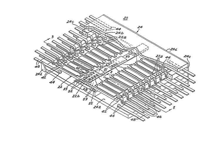
Referring now to Figure~ 1, 2 and 3, a switch 20
includes a unitary bimorph pieæoeiectric element 22 astened
to a Gase 24 ~ia an anchor 26 mounted on a first inner
~r~ace 24a o the case. A second inner case ~urface 24b i~
dispo~ed parallel to surface 24a, and ~paced therefrom by
sidewalls 24c ~nd 24d, the former shown herein comprising
multiple layers. Case 24 and anchor 26 are illustrated as
comprising a ceramio material. However, depending on
~nvironmental and manufaoturing constraints, case 24 and
anchor 26 co~ld alternatively comprise, for example, an
en~ineering plastic ~ch as ULT~M polyetherimide re~in
(ULTEM i9 a registered trademark of General Electric Co.).
Element 22 includes a plurality o generally coplànar
lS fin~ors ~2a arranged in ~ubstantially coaxial, oppositely
extending pair~ conneGted by an intermediately disposed
spine 22~. As shown in detail i~ Figure 2, each finger 22a
i5 separately controllable and includes parallel disposed
upper and lower ceramic plate elements 28 and 30, respec-
tively. Plate elements 28 and 30 are sandwi~hed betweenupper and lower metal layers 32 ~nd 31, resp~tively, ~nd in
turn sandwlch a pair of electrically connected ~etal layçr~
36 and 3~ whi~h ~re fastened to a metal sprin~ layer 39 by
intervening layers of epoxy 40 and 41, re3pectively. The
ele~trical connection between motal layer~ 36 and 38 i~
Chow~ ~c~ematically at 41 in Figure 2. Separate meta~
layers 32 and 34 ~re di3po~ed on each element ~inger 22a for
~eparately polin~ tha elemont flngor~ in a manner well Xnown
to tho~e skilled in the art. M~tal layer~ 36 and 38 and
sprlng lay~r 3g ~re common to spine 22b and all fingers 22a
of ele~ent 22. Metal layer~ 32 and 34 terminato Rhort of
~pine 22b ~u~h t~at the ~pine remain~ unpoled durlng ope~a-
tion of ~witch 20.
~n.~ lff ;L~ 'N~A~ 'H~ 0: lO ~8 ~l 80
. ~ ,, " ~"~, ~, ,~,"~,~
12691Z9
Element 2~ compri~es conventional materials known
to those skilled in the art, incl~ding the multi-layer,
capa~itor-like ~brication approac~. Plates 28 and 30
com~rise, for example, lead zirconate titanate, barium
titanite, ~r other known pie20electric ceramic materials.
Metal layers 32, ~4, 36 and 38 compri~e, for example,
nickel, silver or o~her conventional conduc~ive materials.
As will be appreciated by tho~e ~killed in the art, the use
of electri~ally connected metal layers 36 and 38 sandwiched
about ~pring layer 39 wi~h epoxy layers 40 and 41 produce~ a
ben~er element having ~ub~tantial for~e and resilience.
How~er, as will also be appreciated by those skilled in ~he
art, this center sandwich can be replaced by a single
conductive layer. To decrease the complexity of the draw-
ings and more clearly illustrate the invention, the detailed
cross-section of element 22 is shown only in Eigure 2, and
the thickness of metal layerq 32 and 34 has been exaggerated
in all the Fiyure~.
Ea~h element finger 22a supports a separate
movable contact 42 in the form of a stud extending through
the ree end of the finger opposite spine 22~, and spaced
~rom ~etal layera 32, 34, 36 and 3~, and ~pr~ng layer 3g.
Flr~t and ~cond 3eparatc stationary electrical contacts in
the for~ of pad4 44 are dl~po~ed on surfacec 24a and 24b o~
ca~e 24 opposite each mova~le con~act 42. Separate flexible
conductor~ 46, for example compri~in~ thin copper laysrs,
extond through t~e ~ideo 24c of ca~e 24 and into eloctrlcAl
contact with each contact 42 for making external electrical
conn~otion~ thoreto. Similarly, s~para~ cond~ctor3 48, fox
example comprising coppcr lea~s plated on ceramic c~se 24,
extcnd th~ough s~des 24~ of t~e case and i~o electrical
contact with each p4d 44 for maklng external electrlcal
con~octions thereto. ~eans for applyln~ a s~parate
~0~ `lV .L~ 'N~A~ 'H~ ~d ~0: 10 ~8 ~-l 80
~-- ~v~
~269~29
electrical potential to each element finger 22a include~
electroni~ circuit elements 50 mounted on the upper sur~ace
of spine 22b via an intermediately di~posed layer of
adhesive metallizat.ion 51, metal layer 51 being lnsulatingly
~pac~d from metal layer~ 32. Circuit elements 50 compri~e,
for exa~ple, hi~h voltage integrated circuit devices of the
type comprising ~oth low voltage logic and high voltase
drive circuitry on a single chip. A 6ep~rate met~l lead S2
exte~ds betwee~ each me~al layer 32 and 3~ on each ~in~er
22a, ~nd a corre3ponding connection on one of circuit
eleme~t~ 50, for making electrlcal connection therebetween.
A~ i~ clear f~om a con~ideration o~ Figures 1 and 3, a
plùralit~ o metallized leads 53 exten~ ~e~ween element 22
and anchor 26 for making electri~al connection bet~een
ci~cuit elements ~0 and lower layers of metallization 34.
Connection is made ~e~ween lea~s 53 and c~r~uit ele~ents 50
via leads 52 at the edge of element 22. The gap 54 b~tween
element 22, anchor 26 and leads 53 is optionally ~illed with
epoxy. Gap 54 i~ shown exaggerated in size due to the
~xa~erated thickne3~ of metal layers 32 and 34. Pads 55
are provided on anchor 26 for making electrical connection
bstween cl~cuit eloment~ 50 and external electric~l control
31~nals (not 3hown~ v14 leadY S2. ~lectrlcal connectlon is
made between pads SS and e~ternal circuits (not shown) by,
for exampLe, provi~lng a eonductlve metal bore ~not ~hown)
extendin~ between the pad and the bottom of case 22 through
anchor 26 u3in~ som~conductor fabrlc~tion technlque~ well
k~own to tho~e ~killed in ~e art. Con~uctors and eL~c-
trodcs i~ the signal con~tol path, such as leads 52, 53,
need not have low ohmic value~. 3ecause of the low current
and high impedance nature o~ piezoelec~rlc element 22, tho~e
~ignal control pat~ conduetors c~n compri~s non-metals such
as thicX f~lm conductor pattern~.
-7-
80d lV L~ 'N:~IA3 'H~LI~ ld ~0: 1 0 ~8 ~1 80
~--LO, / ~
` ' 1269129
In operation, circuit element~ 5~ are used to
appl~ a ~ommon electrical potentlal to electrically connect-
ed metal layers 36 and 38, and a sep~rate electrical poten-
ttal to metal layer~ 32 and 34 of each finger Z2a. Each
separate element finger 22a operates independently as a
bimorph piezoelectric bender in a manner well known in the
art, and i~ caused to deflect and force its movable contact
42 into electrical contact with t~e opposing stationary
contact 44 on surface 24a or surface 24b, depending on the
polarity of the ~oltages applied to metal layers 32, 34, 36
~nd 38. Subeequently, when selected movable contact 42
make~ electrical contact with the selected opposing station-
ary contact 44, an electri~al path is established ~etween
the corresponding con~uotors 46 and 4a. When voltage is
lS r~moved from both metal iayers 34 and ~6 o~ a finger 22,
that fin~er returns to the neutral position shown in Eigures
1 and 3. Becau~ spine 27b is left unpoled, there is
minimal flexing of element 22 proximate circuit elemen~s 50
or anohor 26, there~y preventing separation between the
element a~d th~ anchcr or circuit elements and increasing
the life and reliability of switch 20.
While eloctronl~ circ~it ~lement~ 50 have been depicted a3
~hip~, it i~ under~tood that the lnvention 18 not sc limit-
od, a~d di~crcte components can also bo used.
Eigur~ 4 showo a ~wlt~h 420 ~ubsta~tlally ldenti-
cal to switch 20 (Fiqur~s 1-3), wlth the exception of ~he
~onctruction of movable con~act 442 and the elcctrlcal
con~ec~ion3 th~reto. ~ike element-~ are indlc~ted by like
refersnce n~merals incremented by 400~ In this embodiment
~f the lnvention, eaeh movable contact 422 com~rises a metal
clip of qenerally circular cross-sectlon cllpped onto the
end of i~ corre~ponding element finger 422a and ~pace~ from
metal laysr~ 432 an~ 434. A flexlble printed circult board
-8-
60d 1~ N `A~E 'H~LI~ d ~0: 10 ~8 ~l 80
1269123
460 is di~posed in ca~e 424 and includes a separate electri-
cal conductor for making electrical connection between each
movable contact clip 422 and a corresponding, separate pad
464 or conductor (not shown). A seplrate connection (not
shown) is sub~equently made to each pa~ 464, for example
u~in~ a conduc~or simil~r to 48 of Figures 1-3, ~or making
external connections to pads 46~.
Operation of ~witch ~20 is identic~l to that
described for switoh 20 (Fi~ures 1-3) above. The alternate
construction of movable contacts 442 and the use of printed
circuit board ~60 permits the movable contacts to be abrica-
ted ind~pendently from element 422 and easily assembled
th~r~on durin~ the subseguent a~q~m~ly proce~s.
Figure 5 shows a switch 520 substantially identi-
cal to switch 20 (Figures 1-3), with the exception of t~e
co~struction of a movable cohtact assembly 542. Like
elements are indicated by like reference numerals incremen-
~ed by 500. In this embodiment of the invention, each
mova~le contact sssembly 542 comprises a pair o~ contacts
542a spaced from metal layers 532 and 534, respectively, by
intormediAt~ly di~pose~ la~ers 468 o~ insulatin~ material.
~heoe metal contact~ are connected by 4n electrical conduc-
tor 5~ wrapped around the ~ip of element finger 522a and
~paeed from motal layer~ 536 and 538 and the cond~ctive
~S center laye~s o flnger 522a (not ~how~ lexlble electri-
cal conductor 546 i3 ~i~po3cd in contact wit~ movable
contact a~s~mbly 542 for maXlng external electrical connec-
tion thereto.
T~e operation of 3witch 520 i3 8ubgtantially
i~entica~ to that o~ ma~rix ~Wltch 20 (Figure~ 1-3~. The
u~e of insul ~tin~ 1 ayor~ 46~ underneath contact p~d~ 524~
permits metal laye~ 532 and 534 to extend ~ubgta~tially to
th~ tip Of ol~ment fingero 522a, provldin~ the ~lement
_g~
Oid lV .L~I- 'N:~IA~ 'H~LI~ 0: 10 ~8 5v1 80
12691Z9
fi~gers with a stronger de~lection force. Further, the
thickneqs of in~ulating layers 468 between the layers of
metallization and the metal pads can be varied to subse-
quently adju~t the spa~ing between movable contacts 542a and
stationary contacts 544.
Figures 6 and ~A illustrate a switch 620 substan-
tially identical ~o ~witch 20 ( Figures 1-3 ), with the
~xception of the con~truc~on of electrical conductor~ 646.
Like features are indicated by like reference numerals
incremented by 600~ In this alterna~e embodiment of t~e
in~ntion, electrical conductors 646 are plated on element
fi~e~s 622a ( spaced from the metal layers thereon), anohor
626 and case surface 624a. Each electrical conductor 646
termi~ates in a re~pective pad 646a disposed on ~urface 524a
of ~ase ~4. Sub~equent electrical connections~not s~lown),
for example in the form o~ conductors 648, are m~de to pads
6~6a to ~ccommodate external electrioal connections.
Operation of ~witch 620 i~ sub~tantially identical to that
of ~wit~ ~0
Fi~lres 7 and 7A ~how a switch 720 su~atantially
identical to swit~h 20 (Figures 1-3) with the exception of
the con~truction ~f the movable and stationary cont~ct~ 742
and 744. ~ike featureq Are indlcated by like reference
numerals incremented by 700, Various, previously de~ribed
~etails of the matrix swCtch have ~e~n.omitted from the
a~r~wing for t~e purpo~e o~ clearly illustr~ting the c~anged
features. In thi~ embodiment o~ the inv~ntion, each element
fin~er 722~ suppo~ a palr o~ separate movable contacts
742a,742b in t~e form of a pair of separate ~tud~ extend~ng
through the element flnger. Each element flnger 722a is
3hown wlt~ an optio~al bifurcation 780 p~oximate it~ tip
extending vertlc~lly thr~ugh the element finger betwee~ ~o
mo~able cont~ct pair. Further, a ~eparate pair o
- 10-
~L~ 'N~A~ 'H~LI~ 0: IQ ~8 ~l 80
1269~29
stationary contacts 744a and 744b is dieposed on each of
case surfaceo 724a and 724~, opposite each pair of movab~e
contacts 742a and 742~, respectively
The operation of switch 7~0 is ~ub~tantially
id~rltical to ~hat of switch 20 (Figuree 1-3) with the
exception that each element finger 722a switches two sepa-
rate movable contacts 742a and 742b into ~elective contact
with two 3eparate pairs o stationary contact-~ 744a and
74~b. Switch 720 thus makes available twice as Tnany
awitcha~le connections as switch 20 of Figures 1-3. Biur-
catin~ cuto 780 permit movable contacts 742a and 742b to
vary olightly in thei~ flected distance and make good
electrical contact with the respective, opposing stationary
con~act 744a,744b. This bi$urcated construction thus
accommodates minor manufactu~ing deviations, for example in
the relative thickness of the various contacts, which might
otherwise interfere with the establishing of good ntechanical
ancl electrical connections.
Fi~r~ 8 and 8A al~o s~low an alternate em3Oodiment
of switch 20 (Figur~s 1-3) wherein the drawing~ have been
simplifi~d to better illustrate the alternate construction
o movable contacts 842a and 842b and Stationary contaCts
844a and 844b, Ll~e features are ls~dicated by like refer-
ence numoral~ ln~r~mented by 800. In thi~ e~}:odiment of t~e
inventlon, each eloment flnger 822a supports two ~eparate,
r~ctan~ularl~ ohaped movable contact3 a42a and 842b, one
cont~ct 8~2a being dispoeecl on the top surface of each
el~ment 1nger, arid one contact 842b 'ooin~ di~posed on the
bottom Rurace of each element finger (a~ viewed in ~igurea
5 and 8~). Orle palx of ~tat~onary contact~3 844a i3 dlsposed
on case surface 824~ oppo31~o each movable contact 842a.
Similarly, one pAir of ~tationary contact~ 844b i5 dispo~ed
on case surfaco 824a opposlte each movable contact 842b. It
Z l ~ 1~ L~ 'N~A~ 'H~LI ~ 0: 1 0 ~8 ~ 1 8 0
lZ69129
will be understood that in the embodiments of the invention
~hown in the simplified drawings for Eigures 7 and 8, the
movable contacts are spaced or in~ulated from the layers of
metal on the element ingers as in the previo~s embodiment~
described hereinabove.
In operation, movable contacts 842a and 842b act
to electrically bridge and thus short circuit the opposing
pair of stAtionary contacte, thue establishing an electrical
conn~ction selec~ively between conductor pair~ 844a or
conductor pairs 344b.
~ igure 8B shows an alternate embodiment of element
finger 822a and movable contacts 842a and 842b, and is
enlarged to better illu~r~te detail. In thi~ embodiment o
the invention, each finger 822a includes a vertically
extend1ng bi~urcation 822d. Each movable contact comprise~
a ~enerally U-shaped plate ed~ing bifurcation 822~, spaced
rom the metal layers on the finger (only metal layer 83Z
being visi~le in Fi~ure 8), and termi~ating in two pads 842c
at the tip o the finger, one pad on each side of the
bifurcation. Metalli2atio~ layers ~32 and 834 (not visible
i~ Fisure 8B) can option~lly terminate short of bifurcation
822d, leaviny the tip of elomen~ ~inger.822~, proxlmate the
~i~urcation, unpoled. The oper~tion o~ thi~ embodlment of
the lnventlon i~ ~ubstantially identlcal to that o~ Figure~
~ ~nd 8A a~ove, wlth bifurcation 822d accommodating minor
manufactu~ing deviations ~y permlttin~ some flexibility
proximate the ~ree end of finger 322a in a manner slmilar to
that de~crlbed for F~gures 7 and 7A above.
There i~ thu3 provided alternate cmbo~lmen~ of
swltch, ench o~ which use~ a bimo~ph piezoelectric bender
element in a compact, comb s~apod configuration to provide
3ep~rate control ~f multlple, closely ~paced, ~wltchable
Qloctrlcal contAct~. The 4witch i~ light in welght, ~mall
~Id 1~ [ 'N~IA~I 'H~ d ~0: 10 ~8 ~1 80
iZ~9:129
in size, and can b~ constructed using known fabrication
technologie~. Precision semiconductor microcirc~it fabrica-
tion technique~ can be used to manufact~re lar~e quantities
of these switches with reliable, repeatable, close-tolerance
features. The nature of the switch provides a high degree
of electrical isolation, and hence low cross-talk, between
-witched ~i~nals even at requencies approaching t~e mega-
her~z range. ~urther, each embodiment of the switch has a
low actuator pewer ~eq~irement, and comprises sturdy,
reliable component3. As is shown in the multiple em~odi-
ment~, the exact nature of the contact co~ctruction and
~ence the switchin~ operations c~n be tailored to specific
opera~ional an~for manufacturin~ requirements. Further, the
incl~sion of electronic circuit elements on the piezoelect~ic
element and within the case provides a substantially
self-contained unit with the attendant advantage-c of ease of
ins~allation a~d servic~ability in a compact package.
While a preferred e~bodiment of the inventio~ has
been illustrated and desc~ibed, it will be clear that the
invention i~ not so limited. For example, while the embodi-
ments o the invention illustrated and de cribed herein
includR m~ltipl~ pai~ of gen~rally co~x-ial and oppo~l~ely
~xtending finger~, it wlll be ~ppreciated that the inventlon
i8 not ao limited. A switch con~tructed ln accor~ance wlCh
t~e pregent ~nVention coul~ compri~e, for example, a slngle
element finger extendl~g oppo~ite of two or more fin~erY, or
any other combinatlon of oppo~ltely extendlng fingers.
~urther, while the ombod~ment3 ~hown and describe~ abo~e
each include at least two stationary cont~cts ll.e., one on
30 a ca e upper 4urface and o~e on a case lower su~face)
oppo~ite eich mov~ble con~act, lt will be appreciated by
tho~a 3k~11ed in the a~t that ~he in~ention i9 equ~lly
appli~ble to ~wltc~e3 in ~hich only one statlonary contact
-13-
~1~ .L~I 'N~A~l 'H~ ld ~0: 10 ~8 ~l 80
lZ~i~lZ9
opposes each movable contaet (i.e., a single-pole,
single-throw switch configuration). Numerous modification~,
changes, variation~, substitutions and equivalents will
occur to those ~killed in the art without departing from the
spirit and scope of the present invention. Accordingly, it
i5 in~ended tha~ the in~ention herein be limi~ed only by the
~cope of ~he appended claims.
-14-
~ t ~ 1 'N3A3 'H~ * ~ 0: 1 0 ~ 8 ~ I 8 0