Note: Descriptions are shown in the official language in which they were submitted.
- ~2~jC31~5
WC17/25
RADIANT BEAM COORDINATE DETECTOR SYSTEM
The present invention relates to a radiant
S beam coordinate detection system, more
particularly, to a crossed infrared beam coordinate
detection system.
Crossed infrared beam X-Y coordinate
detection and encoder systems are well known in the
10 art. See U.S. patents 3,764,813; 3,775,560;
3,860,754; 4,243,879; 4,267,443; and 4,384,201, for
example. Typically in these systems x and y
coordinate arrays of paired -nfrared light sources
and detectors are caused to scan a display surface
with crossed light beams by an electronic scanning
system. When any of the beams are interrupted the
prior art detection systems are equipped for
determining the position of the interrupted beams.
Problems encountered in the design of a
crossed radiant beam coordinate detection system
such as those described above include: ambient
light interference which produces radiation in the
IR spectrum that can interfere with operation of
the system; wide variation in performance of
optoelectronic devices due to differences in
optical and mechanical axes; aging of emitters
which reduces their output; scattering, reflection,
and attenuation effects due to the housing used for
mounting the emitter/detection pairs; and the
optical alignment of emitters/detectors.
31~r5
-2- WC17/25
U.5. patents 3,764,~13, 3,775,56b and
3,860,754 disclose systems in which the arrays of
emitters and detectors are electronically
sequentially scanned. This helps reduce problems
due to emitters/detectors being non-aligned and the
effects of scattering, reflections etc.
U.~ paten~ 4,243,879 discloses a means for
compensating for ambient light fluctuations in the
performance of crossed beam coordinate detection
10 and encoding systems, while U.S. patents 4,267,443
and 4,384,201 disclose among other things a means
for determining the relative size or center line of
the object which is interrupting the beams.
Despite the advantages of the above described
systems a need still exists for an improved crossed
beam coordinate detection and encoding system which
addresses the above problems with greater
flexibility.
An object of the present invention is to
provide an improved crossed beam coordinate
detector and encoding system which provides for
greater flexibility of performance.
The present invention relates to a crossed
radiant beam ~-y coordinate detection system. The
crossed radiant beams in the preferred embodiment
are provided by a plurality of emitter and detector
pairs located along each axis of a display space.
The crossed infrared light beams are amplitude
modulated and caused to scan the display space.
Means are provided for detecting an interruption of
the crossed light beams in response to the presence
or absence of the amplitude modulation.
The detectors are operated over a wide
dynamic range and this in combination with the
~2.~j91'~ 5
_3_ WC17/25
envelope detection of the amplitude modulation
provides means for eliminating ambient light
interference as long as the detectors are operated
within their dynamic range. The output of the
envelope detector is coupled to a high gain
amplifier which helps to compensate for tolerance
and aging of the electronic components and inherent
misalignment problems.
The present invention further relates to a
crossed radiant beam x-y coordinate detection and
encoder system that includes a plurality of emitter
and detector pairs along each axis wherein the
crossed light beams are caused to scan a display
space and means are provided for detecting the
interruption of the light beams. Further, the
system comprises means for repeatedly reporting
coordinates associated with the interrupted light
beams which are present over a series of display
space scans, the reporting taking place over
preselected scan intervals. In the preferred
embodiment, two scanning intervals are provided; an
initial scan interval of time Tl; and subsequent
scan intervals of time T2.
The reporting means further comprises
xeporting immediately when the interrupted beams
have disappeared. However, the system includes
means for locking out the repeated reportings of
the continuously present interrupted beams and the
disappearance of interrupted beams beyond the
initial reporting of the coordinates of an inter-
rupted beam as they first occur, the locking out
means operating in response to the position of the
interrupted beams in a selected display space.
The reporting means of the detection and
encoding system further includes means for
WC17/25
--4-
reporting the minimum and maximum coordinates of
the interrupted beams for each axis and for
reporting the average x and y values of the
interrupted beams. Means are further provided for
reporting an error when the interrupted beams along
either of the axes are either too small or too
large based on the min and max or average values
reported.
The coordinate detection encoding system of
the present invention further comprises a
diagnostic means for checking the operation of each
emitter/detector pair and for checking the scan
speed of the system. Further, the checking of the
emitter/detector pairs can take place at either a
lS normal power level or at a reduced emitter power
level to check for marginal performance.
FIG. 1 is an overall block diagram of the
present invention crossed beam coordinate detection
and encoding system.
FIG. 2 is a more detailed block diagram of a
light emitting and associated driving circuit
portion of the system of FIG. 1.
FIG. 3 is a more detailed block diagram of a
detector circuit portion of the system of FIG. 1.
FIG. 4 is a more detailed block diagram of a
receiver circuit portion of the system of FIG. 1.
FIG. 5 is a more detailed block diagram of an
amplifier portion of the receiver circuit of FIG.
4.
FIG. 6 is a block diagram showing a
microprocessor controller portion of the present
invention of FIG. 1 coupled to a main processor
portion over a bi-directional 8 bit bus.
FIG5. 7A and 7B are a block diagram of a
t~S
WC17/25
--5--
program for controlling the system of FIG. 1.
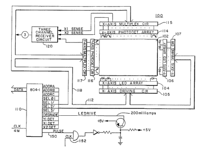
Referring to FIG. 1, a preferred embodiment
crossed beam coordinate detector and encoder system
designated generally 100 is shown. It comprises a
display space 102 to be scanned by the crossed
beams generated by the x-axis array of LED emitters
104 and corresponding driving circuit 105 lying
along one side of the display space 102 and the
y-axis array of LED emitters 106 and corresponding
driving circuit 107 lying along another side of the
display space 102, all under the control of the
microprocessor controller 110 via bus portion 112.
In the preferred embodiment there are forty-eight
LED's along the x-axis and 32 LED's along the
y-axis, although almost any number of LED's can be
used depending on the design re~uirements of the
system.
The system comprises a corresponding array of
48 photodectors 114 and corresponding multiplexer
circuit 115 lying parallel to the x-axis array of
LED's 104 on an opposite side of the display space
102 therefrom. Similarly, there is an array of 32
y-axis photodetectors 116 and corresponding
multiplexer circuit 117 lying parallel to the
y-axis array of LED's 106 on an opposite side of
the display space 102. The photodetectors and
multiplexing circuits of each array are controlled
by controller 110 via bus portion 118. The LED's
and photodetectors of each parallel array are
paired together.
The interruption of a beam or beams during
scanning is detected by a receiver circuit 120.
Detection of interrupted beams by the receiver
circuit is transmitted to the controller 110 by the
91~5
WC17/25
--6--
bus portion 118.
Referring now to FIG. 2, the x-axis LED array
and driving circuit comprises 48 LED devices LEDl
to LED48, and decoder driver circuits even numbers
202 through 212. These are standard TTL 7445
devices. There are six decoder driver circuits,
each are coupled to eight of the LED's, e.g.
decoder driver circuit 202 is coupled to LEDl-LED8.
Each of the decoder driver circuits 202 through 212
receive three address lines ADDRA, ADDRB and ADDRC
from the controller llO (an Intel~ 8041
microprocessor controller in the preferred
embodiment) over the bus portion 112. The three
address lines define which of the eight LED's
attached to the decoder driver circuit will be
activated. Signals SEL0/,SEL1/,SEL2/ and SEL3/
from the controller 110 are used to select which
decoder driver circuit is enabled. These select
signals are active low and only one signal is
active at a time.
The y-axis LED array 106 and driving circuit
107 is similar in design. The same address and
select signals as described above are
simultaneously transmitted to the y-axis driving
circuit 107 and LED array 106. However, since in
the preferred embodiment there are only 32 y-axis
LED's only four decoder driver circuits are used.
It can be seen from FIG. 2 that when either SEL0/
or SELl/ are active there will be two x-axis LED's
on for each y-axis LED. When SEL0/ is active low
both circuits 202 and 210 are enabled while
circuits 204 and 212 are enabled when SELl is low.
For example, when LEDl is active so is LED33 and so
on as when LED16 and LED48 are activated.
Thereafter during the remaining part of the scan
9~
WC17/25
--7--
(LED17-LED32) only one x-axis LED is activated for
the corresponding y-axis LED. This accomodates a
scan of a 32x48 array in a shorter amount of time.
Correspondingly, the address and select
signals are transmitted simultaneously along bus
portion 118 to both the x-axis multiplexer circuit
115 and the y-axis multiplexer circuit 117.
Referring to FIG. 3, the x-axis multiplexer circuit
is shown in detail. An array of 48
phototransistors PTl-PT48, are shown coupled to six
multiplexer circuits even numbers 302 through 312.
Suitable multiplexers are made by RCA with the
model no. 4051. Multiplexers 302 through 308 have
their common output line coupled together to the
emitter of transistor 320 while the common output
of circuit 310 and 312 are coupled to the emitter
of transistor 321.
When a particular LED of the x-axis LED array
is activated a corresponding phototransistor is
multiplexed onto one of the two common output lines
and transmitted to the emitter of either transistor
320 or 322. For example, when LEDIs 1 and 33 are
fired simultaneously, the multiplexer circuits 30
and 310 make the outputs of phototransistors PT1
and PT33 available to the emitter of transistors
320 and 322, respectively. The collector outputs
of the transistors 320 and 322 are coupled via
lines Xl Sense and X2 Sense, respectively, to the
receiver circuit 120.
Similar circuitry is used with the y-axis
phototransistor array 116 and multiplexer circuit
117 except that there are only 32 phototransistors
and four multiplexer circuits. Their common output
is coupled ~o the emitter of transistor 402 in FIG.
4 whose collector output is provided as a Yl sense
-
~ ~`)9:~S
WCl7/25
signal to receiver circuit 120.
Remembering the description of FIG. 2, the
controller 110 through the select lines enables one
of the decode driver circuits (or a pair of
circuits if SEL0/ or SELl/ is low for the x-axis
driver circuit 105) and through the three address
lines chooses a particular LED of the eight coupled
to the enabled decode driver circuit to be
activated for each axis. Then the controller turns
on the chosen x and y emitters by generating a high
pulse signal 150 in FIG. 1 and modulating it with a
29 kHz clock 152. This signal is coupled to the
base of transistor 150 and its collector provides a
29 kHz modulated LE~ drive signal over bus portion
112 to the LED's of both the X and Y axis arrays
104 and 106, respectively. See the LEDRIVE line in
FIG. 2. By designing an appropriate envelope
detector receiver circuit this 29 kHz carrier helps
to alleviate all types of interference including
ambient light interference.
Referring now to FIG. 4, a more detailed
schematic of one channel of the three channel
receiver circuit 120 of FIG. l is provided. All
three channels are substantially the same so the Yl
channel is chosen as representative. The emitter
current of the chosen phototransistor of the x-axis
array 106 and multiplexer circuit 107 is coupled to
the emitter of transistor 402 as described before.
The collector of the phototransistor for both the
x-axis and y-axis arrays 114 and 116, respectively,
are coupled through a relatively small 470 ohm
resistor to a 5V source. This provides for a wide
dynamic range in response to incoming light levels
resulting in high immunity to high levels of
ambient light by avoiding saturation of the
145
WC17/25
phototransistor. Transistor 402 has a grounded
base which provides the speed required by the 29
kHz carrier and additionally provides amplification
at low levels of ambient light.
A voltage swing is developed across 9.1 K
load resister 404 which swings from a negative
voltage when there is no light on the chosen
detector, that is, when the beam is interrupted, to
near 5 volts when the detector saturates. However,
to avoid DC saturation at the collector, to
compensate for the increased sensitivity of the
detector, and to limit the switching spikes
generated by the multiplexers, a non-linear load is
added in parallel with resistor 404 to the
collector load. This non-linear load comprises 220
ohm resistor 406 in series with a lN4152 silicon
diode 408 and 620 ohm resistor 410 in series with a
G866 germanium diode 412. These two parallel
resistor-diode pairs tend to clamp the output
voltage when the detectors receive more light and
during multiplexer switching.
The voltage developed on the collector of
transistor 402 is AC coupled via 1 nanofarad
capacitor 420 to the analog integrated circuit (IC)
amplifier designated generally 500 and described in
more detail in connection with FIG. 5. The
capacitor 420 blocks the 60 or 120 Hz component
generated by artificial ambient light but allows
the 29 kHz carrier through. The signal from the
collector of transistor 402 after passing through
capacitor 420 is coupled to pin 7 of IC amplifier
500. The diode and RC network coupled to pin 7
further reduces multiplexer spikes by clamping to
the average input.
The IC amplifier 500 was designed to detect
12f~1" 5
WC17/25
--10--
the presence or absence of infrared carriers, in
particular, in remote control applications. It is
available from NEC, Model No. 1373, or Motorola,
Model No. 3373. It comprises an 80 dB amplifier
502 with automatic bias control 504, followed by a
limiter 506, a peak detector 508 with threshold
adjustment, and output shaping 512. The gain of
the IC amplifier 500 is defined by the ratio of the
impedance of the load at pin 3, divided by the
impedance at pin 6. The IC amplifier 500 can
operate on wide band (with resistive loads), or
narrow band (with tuned circuits). In the tuned
embodiment a tuned circuit comprising a parallel
430 ohm resistor 440, an inductor 442, and a 2.2
nanofarad capacitor 444 are provided in FIG. 4. In
the preferred embodiment, however, a resistive load
is provided by removing inductor 442. The load at
pin 6 is a 3.9 ohm resistor 446 coupled to ground
through 4.7 microfarad capacitor 448.
The output of the peak detector is compared
at pin 4 in FIG. 5 with a fixed threshold set by
the circuit 450 in FIG. 4. After passing through
the shaping circuit 512 the output of the circuit
500 on pin 1 is converted to a TTL compatible
signal and buffered by gate 460. This output,
YDET, is high/low co.rresponding to the presence or
absence of a beam.
Two additional receiver channels like the one
described above in connection with FIGS. 4 and 5
are provided for the Xl Sense and X2 Sense signals
received from the collectors of transistors 320 and
322 in FIG. 3. The only difference is the
selection of the values for the 330 picofarad and
9.1 K resistor 404 coupled to the collectors of
402. In the Xl and X2 Sense channels these values
,Cj
~IC17/25
--11--
are 820 picofarads and 4.7 K ohm, respectively.
These values are different because the distance
between the y axis LED's cmd associated detectors
is greater than the distance between the x-axis
LED's and detectors therefore requiring different
sensitivities in their respective receiver channel
circuits.
A DEGRADE line is provided over bus portion
112 from controller 110 to the x and y emitter
arrays and driving circuits. This line is coupled
through a 180 ohm resistor to the light emitting
diodes, for example diode~ LEDl-48 from the x-axis
array 104. When the controller activates this line
it produces a lower drive for the LED's for
evaluating degradation of the LED's due to aging.
The low 470 ohm load resistance 340 on the
detectors PT 1-48 provides a fast response time and
wide dynamic range. The use of an AM carrier (29
kHz modulation by clock 152 and use of receiver
channel 120) virtually eliminates ambient light
interference as long as the detectors are within
their dynamic range. The use of a high gain (80
dB) AC amplifier with auto bias control (IC
amplifier 500) absorbs overall losses and
variations due to the optical link and components,
aging of the emitters, and variations in assembly.
Referring to FIG. 6, as mentioned earlier, a
single chip peripheral microprocessor 110 is used
to control the system 100. Controller 110
communicates to a main processor 602 (an Intel
80186) on a bidirectional 8 bit bus 604. The
controller 110 has several internal registers
(MCR0-MCR6) that define the operating environment
and system parameters: screen size and format,
repetition rates, scanning speed, operating mode,
31'~ 5
WC17/25
-12~
etc. These registers can be changed by the main
processor 602 at any time. The controller 110 can
perform any of four operations: normal screen
scan, internal registers dump, diagnostics on the
controller or the system, and a do nothing.
The controller 110 has 64 bytes of RAM and 1
K bytes of ROM plus an 8 bit internal
timer/counter. It communicates with the main
processor 602 on the low byte of the main
processor's data bus (D0 to D7) through a set of
three registers: DBIN 606; DBOUT 608; and STATUS
610.
The main processor 602 writes to DsIN 606
which sends an interrupt to controller 110 and sets
the flag IBF by D1 in the STATUS register 610. The
flag IBF will be cleared when the controller 110
reads the data. The content of DBIN 606 can be
interpreted as command or data depending on the
state o~ A~ of the system address bus 607 at write
time which is copied into controller flag register
Fl. ~A~ = 0 means data.) The address bus 607 from
processor 602 is coupled to controller 110 via
decoder circuitry 609.
The data output register 608 when written
into by the controller 110 generates an interrupt
TSINT to the main processor 602 and sets flag OBF
corresponding to DO in the STATUS register 610.
The flag is cleared when the processor 602 reads
the DBOUT register 508. The status register can be
read by the main processor 602 at any time, but it
is a write only for controller 110.
The tasks assigned to controller 110 are to
provide coordinates of an object that intercepts
the beams of the coordinate detection system 100,
and to perform diagnostics of the system. Since in
9~ 5
WC17/25
-13-
general a finger or o~her stylus used to interrupt
beams will interrupt more than one beam along both
the x and y axes, coordinates are calculated as a
weighted average or as the min/max position of the
beams interrupted by the object. The MCR5 register
of controller 110 defines the minimum and maximum
number of beams which must be intercepted in order
to generate valid coordinates for both the x and y
axes~ It also defines whether average coordinates
(one xy pair) or max and min coordinates (two xy
pairs) are to be reported.
Register MCR6 defines which of the previously
enumerated modes the system is in. For example,
the format for MCR6 in the normal mode is as
follows:
D7 D6 D5 D4 D3 D2 Dl D0
* * * 0 1 1 1 0
The meaning of the * bits in the normal mode is:0
standard normal mode 0 0 0
restart (from Tl) X X 1
lockout X 1 X
(An x bit indicates a do not care state.) Restart
and lockout will be described below. In general in
the normal mode of operation, after detection of an
object, the coordinates of the interrupted beams
are generated from knowledge of the address lines,
select lines and value of the Xl, X2 and Y1 Detect
lines. Scanning continues but new coordinates are
not reported until after a Tl time delay has
occurred. This includes not reporting the
ccordinates of interrupted beams upon subsequent
scans if they are still present, unless the
31~ 5
WC17/25
-14-
interrupting object is wi~hdrawn and then this is
reported. Coordinates will be reported at Tl and
thereafter at a T2 rate. Val~es of Tl and T2 are
loaded into MCRl and MCR2, respectively, by the
processor 602.
For some keyboard commands, the operator
keeps his finger in place until a particular value
such as an alarm level has been incremented or
decremented to a desired level. That is why
coordinates are reported every T2 seconds after the
first Tl interval. ~owever, other keyboard
commands are not intended as repeat functions and
the main processor does not wish to be interrupted
by reporting of coordinates associated with those
commands after the initial report. In such an
instance the processor 602 issues a lockout command
which means no further coordinates are to be
reported until an "object gone" and "new object"
are reported.
Referring now to FIGS. 7A and 7B, a more
detailed description of the normal mode of
operation 701 is provided. Initially, the system
is cleared of any interrupted beam reports and a
state flag is set to 0. A quick scan of the
display space is accomplished and if the space is
clear of any interrupted beams 702 and the state is
still zero 704, the process of looking for
interrupted beams begins again.
Upon subseguent scans if interrupted beams
are first detected at 702 and the state is still
zero 703 (that is, there had been no display space
activity in the prior scan), then the state flag is
set to 1 and a delay count is set to Tl 707, the
value loaded in MCR1. Coordinates of the
interrupted beams are generated 708 and error
r 5
WC17/25
-15-
checking 710 is performed.
Error checking is performed by the controller
110 wherever coordinates are generated to determine
if the object is discontinuous along the x or y
axis, i.e. not all beams are interrupted between
the min and max coordinates reported, or that the
object is too small or too big in the x or y
directions. It does the latter by comparing the
number of beams intercepted along each axis with
the min and max values stored in MC~5.
Next, the data along with the error byte is
transferred 711 to the main processor 602. When
reporting average coordinates, the sequence of
transfer is ERROR - BYTE, X, and Y. In the max/min
mode the range of values is 0 to 47 for X, and 0 to
31 for Y. The output sequence is ERROR - BYTE,
MAXX, MAXY, MINX and MINY. The data when
transferred to the processor 602 is flagged with a
byte number indicated at D4, D5 and D6 in the
status register. During data transfer s~anning of
the display space is stopped.
Following the data transmission, when the
controller 110 receives a data acknowledge from
processor 602 the program begins again at 702 to
see if the screen is clear. If the answer is still
no then at 706 the state flag is observed and in
the previous loop it had been set to one. Then
inquiry is made at 712 whether the dump flag is
set. This flag is controlled by the internal
timer/counter of the controller 110 set at 707.
The dump flag is set at time Tl after the initial
generation of coordinates. If time Tl has not
elapsed then the controller does nothing and the
program returns to begin.
Assuming on subsequent passes the screen is
~ 314~ WC17/25
-16-
still not clear and the state is still 1, the dump
flag will be set at time Tl. At time Tl, the state
is set to 2 and the dump flag is set false 714. If
a lockout command is not present 716 then the
coordinates are generated anew 708, error checking
is performed 710 and the data transmitted to the
processor 602. This process will continue as long
as the object is present, but the dump flag will be
set at time intervals T2 thereafter.
If a lockout is present at 716 then instead
of new coordinates being generated the program
returns to begin.
At some point in time at 702 the screen will
be clear but the state will not be zero at 704. If
no lockout is present at 718, then a report will be
made to the main processor 602 that the object is
gone 720. After this the state will be set to
zero, the dump flag set false 722, and lockout
command cleared 724. The program will return to
begin. If a lockout is present at 718 the step of
reporting the "object gone" 720 is bypassed.
Some of the mode control registers were
described above (MCRl for Tl; MCR2 for T2; MCR5
instructions for beam coordinate calculation and
error checking; and MCR6 for operating mode). MCR0
defines the display space format, while register
MCR3 is used for diagnostics.
The control registers are set by a command
from the processor 602 set in DBIN. After checking
the IBF flag the controller 110 loads the command
in a command register. The number of the control
register to be set is set in the lower three bits
of a command. Except for MCR6, commands for
setting the register are followed by a data byte.
MCR6 is set by the upper bits of the command byte
WC17/25
-17--
thereby limiting this most frequent command to one
byte, minimizing the main processor overload.
Operation of the nonnal operating mode and
the sig~ificance of the lockout and restart
commands in response to the command bytes in MCR6
was described above. The other mode of
significance for purposes of the present invention
is the diagnostic mode. First a diagnostics
command byte is sent to the command register. The
format is:
D7 D6 D5 D4 D3 D2 Dl D0
# X X 1 1 1 1 0
Bit # when set selects diagnostics for the
controller, otherwise the diagnostics are to be
performed in the coordinate detection system.
Following the diagnostics command byte a data
byte defining the diagnostics to be performed is
loaded into the MCR3 register. This register
defines the axis under test, the emitter/detector
pair to be tested and indicates if the test is
performed in the degraded mode using the DEGRADE
signal. In the degrade mode a particular
emitter/detector pair is tested at 90% of emitter
output.
Then the scanning rate is checked. Scanning
is the delay time between the time a pair is
selected and the time at which the state of the
scan line is read. The desired scanning rate is
defined by control register MCR4. In the preferred
embodiment the delay between placing an address and
reading the state of the detect line is 900
microseconds. This number is as fast as possible
to reduce response time, but slow enough to operate
~ ~j9145
WC17/25
-18-
reliably. The processor 602 can change the MCR4
setting to test marginal operation.
As a result of a diagnostic test a two byte
report is sent to processor 602 via DBOUT. The
first byte reports on diagnostics performed on the
controller while the second byte reports on emitter
detector failure at normal or degrade state.
To perform diagnostics, the main processor
602 will have to DUMP the internal registers to
read MCRO and MCR4. MCR0 defines the screen
format, and has to be used to generate a valid bit
pattern on MCR3. An invalid pattern will cause an
invalid error report. The default screen format
for the present invention defines a screen size of
32 (Y) by 48 (X) pairs. All elements on the Y axis
are detected on YlDET. However on the X axis
elements 1 to 32 are detected on XlDET line, and
elements 33 to 48 are detected on X2DET. As the
address range is only 0 to 31, to address pair #33,
the address must be 0 and X2DET selected.
~ s mentioned previously MCR0 defines the
display space 102 format. The space is divided in
a number of areas that are scanned simultaneously.
The size of the area and range of validity for X2
Det and Yl Det can be redefined by the register. A
single data byte defines the space format as
follows:
area size (3 to 32) D0 to D3
valid range for X2D ~3 to 16) D3 to D4
size of Y on Y axis (3 to 32) D5 to D7
At the end of any report from the controller
110 (e.g. coordinates, diagnostics, register dump)
the byte number on the status register goes to
L~ S
WC17/25
--l"--
zero, and a dummy data byt:e from the processor 602
i5 expected, as a handshake (data is don't care).
The handshake assures that the main processor 602
will not be interrupted with a new set of
coordinates etc., before it is ready for them. The
controller 110 will be on a do nothing loop until
this byte is received.
Referring back to FIG. 7, the main processor
602 sets the mode as stop, normal, dump or
10 .diagnostic 700. If normal mode is selected 701
then the controller proceeds to 702 and this
portion was described earlier. However, if the
processor 602 wishes to perform diagnostics it
first calls for a dump 730 in which all the control
registers are read 732. Then the controller stops
734. The processor 602 then commands a diagnostic
740 which is performed 742, and the report bytes
are generated and reported to the main processor
746. The controller stops 748 and awaits the next
command.