Note: Descriptions are shown in the official language in which they were submitted.
1~9163
rhotodcteetor
The present invention relates generally to a photodetector
and more particularly to a photodetector suited for use as an
optical pick-up head for optically recording or reproducing
information on or from an optical information carrier medium.
A video disc system is known wherein information recorded
on an optical information carrier medium, for example, a video
disc, is optoelectrically reproduced. In general, this video
disc system makes use of an optical pick-up head and a laser
as a source of light to be eventually detected by the pick-up
head.
To enable the prior art to be described with the aid of
diagrams the figures of the drawings will first be listed.
Fig. 1 is a schematic side view of a photodetector
according to a first embodiment of the present invention;
Fig. 2 is a side view, on an enlarged scale, of a portion
of the photodetector shown in Fig. l;
Figs. 3 and 4 are side views of a photodetector according
to second and third embodiments of the present invention,
respectively;
Fig. 5 ls a graph showing a characteristic of a photo-
detector according to the present invention;
Fig. 6 is a graph similarly showing another characteristic
of photodetectors according to the present invention;
Fig. 7 is a schematic diagram showing a typical optical
'~
12t~91~3
. , .
-- 2
head system;
Fig. 8 is a schematic top plan view of a conventional
~ photodetector;
Fig. 9 is a schematic side view of the photodetector shown
in Fig. 8;
Fig. 10 is a circuit diagram showing tracking signal
processing circuitry;
Figs. ll(a) and ll(b) are diagrams showing the waveforms
of signals appearing in the circuit of Fig. 10;
10Figs. 12 and 13 are diagrams showing temperature-
dependent characteristics of tracking error signals;
Fig. 14 is a schematic side view of a photodetector,
used to explain the interference of light;
Fig. 15 is a schematic side view of a photodetector
according to a fourth embodiment of the present invention;
Fig. 16 is a schematic side view, on an enlarged scale,
of a portion of the photodetector shown in Fig. 15;
Fig. 17 is a schematic side view of a photodetector
according to a fifth embodiment of the present invention;
20Fig. 18 is a schematic top plan view of a photodetector
according to a sixth embodiment of the present invention;
Fig. 19 is a side view, on an enlarged scale, of a portion
of the photodetector shown in Fig. 18;
Fig. 20 is a schematic side view of a photodetector
according to a seventh embodiment of the present invention;
Fig. 21 is a schematic top plan view, on a somewhat
reduced scale, of the photodetector shown in Fig. 20;
Fig. 22 is a perspective view of a photodetector
according to an eighth embodiment of the present invention;
30Fig. 23 is a schematic side view of a photodetector
according to a ninth embodiment of the present invention;
Fig. 24 is a schematic top plan view of the photodetector
shown in Fig. 23; and
Fig. 25 is a perspective view of a photodetector according
to a tenth embodiment of the present invention.
Fig. 7 illustrates a popular example of an optical pick-
up head system, wherein reference numerals 1, 2, 3, 4, 5, 6,
7 and 8 respectively represent a semiconductor laser, a
12~;91~3
. ~ .
-- 3 --
diffraction grating, a beam splitting prism, an objective lens
assembly, a concave lens, a cylindrical lens, a photodetector,
and a video disc. The control system used is a three-beam
tracking control system, wherein a tracking error signal can
S be detected by a pair of photocells 7a and 7b in the photo-
detector 7. The focus control is an astigmatism system, where-
in a focusing error signal can be detected by a four-segment
photocell 7c. An information (RF) signal can be detected by
the four-segment photocell 7c.
In this type of optical pick-up head, the photo-detector
7 is of a type formed by molding a synthetic resin, for
example, transparent epoxy resin, the structure of which is
shown in Figs. 8 and 9. As shown therein, the photodetector
7 comprises a substrate 7d on which photocells 7a, 7b and 7c
are formed, as well as lead wires 7e for feeding respective
outputs from the photocells, and output terminals 7f for
connecting the photocells with an external circuit. All of
said substrate 7d, the lead wires 7e and portions of the
terminals 7f are embedded in a molded transparent resin layer
7g. Built-in functional units are arranged at a substantially
central portion of the molded resin with respective light
receiving faces 7a', 7b' and 7c' of the photocells parallel
to a light receiving surface 7h of the resin layer 7g.
Outputs (currents) from the associated photocells 7a and
7b are converted for tracking purpose into respective voltages
by tracking signal processing circuitry as shown in Fig. 10.
The tracking error signal is obtained from a subtracting
circuit A2 by subtracting the respective outputs of the
photoceLls 7a and 7b. More specifically, assuming that the
outputs (after having been amplified) of the photocells 7a
and 7b are expressed by Sa and Sb, respectively, a tracking
error signal component TE can be expressed by TE = Sb - Sa.
It is to be noted that in Fig. 10 reference characters AO and
Al represent amplifiers. Fig. ll(a) illustrates the respective
waveforms of the outputs Sa and Sb, and Fig. ll~b) illustrates
the waveform of the tracking error signal. Normally, an
intermediate point (1/2 of the value P-P) of the TE signal
does not coincide with the GND level, because of conditions
in the optical system, as well as the difference in DC level
12~i91~3
of the outputs Sa and Sb, and also in the output level. For
circuit compensation for deviation of the intermediate point
either the resistance R4 or Rl, or the resistance R6 or R3, is
adjusted to bring the intermediate point into coincidence with
the GND level.
However, since a tracking servo is apt to function to bring
the intermediate point into coincidence with the GND level in
the event of any deviation occurring between the intermediate
point and the GND level, it will have an offset in the tracking
direction if the deviation exceeds a predetermined quantity,
and in this case the servo will no longer function.
This conventional optical pick-up head has a problem in
that, since it often happens that the tracking error signal
changes with change in temperature to such an extent that the
servo circuit can no longer perform its control function, the
tracking operation tends to become unstable. Fig. 12 illus-
trates a temperature-dependent change of the tracking error
signal, and, as shown therein, the tracking error signal TE
once adjusted at normal temperature undergoes a change with
the temperature T and, at a certain temperature, displaces to
the position shown by TE'. In this connection, assuming that
the amplitude of the tracking error signal is expressed by P
and the displacement of an intermediate point C of the amplitude
of the tracking error signal is expressed by ~x, and when the
rate of change a (=(~x/P) x lQ0%) attains a value higher than
10%, the tracking servo tends to become unstable.
Fig. 13 illustrates the temperature dependen~. characteristic
of the rate of change a in the conventional optical pick-up
head, and it has been found that the change rate a often attains
15 to 20~ at maximum and that, moreover, the change rate a
varies in a swelling fashion at a predetermined interval of
temperature, for example, by the effect of a temperature
difference of 10 to 15C. In Fig. 10, where the initial
adjustment has been made at normal temperature, in which case
the change rate ~ is, as a matter of course, zero (because the
intermediate point coincides with GND level and the value Ax
is therefore ~ero), the change rate a attains a peak
value at a temperature 10 to 15~C higher than the
12~91~3
normal temperature. Accordingly, at a temperature as high as
that at which the change rate ~ exceeds 10%, the tracking
operation tends to become unstable.
It has been found that this problem results from the
interference of light that is attributable to the change in
optical path induced by the change in temperature. The
interference of light is paramount, particularly in the
photodetector, occupying 70 to 80% of all the change rate.
Fig. 14 is a diagram used to explain how the light
interference occurs as a result of a difference in the optical
path. A beam BO of light for trackïng purpose enters the
light receiving surface 7h of the molded resin layer and is
subsequently detected by the photocell 7a. Assuming that the
position of the light receiving surface is located at the
level 7h when the position and intensity of the incident beam
were initially adjusted at normal temperature, when the
temperature increases to a higher value, the molded resin
layer undergoes thermal expansion with the light receiving
surface consequently shifting to the position shown by 7h'.
Let it be assumed that the distance between the light
receiving face of the photocell 7a and the light receiving
surface 7h is expressed by Ql, and the distance between the
light receiving surfaces 7h and 7h' is expressed by ~Q. The
incident beam BO after having impinged upon the light receiving
face of the photocell 7a is partially reflected therefrom
towards the light receiving surface of the molded resin layer,
as shown by B2 or B2', and when and after the distance ~Q
has attained a value that brings about interference of the
light, the reflected light interferes with the incoming
incident beam BO producing a pattern of dark and bright
fringes on the face of the photocell 7a.
It is well known from the theory of the interference
of light that, when two light beams from the same light
source and hence of the same wavelength ~ travel along
respective optical paths of different distances and having a
path difference of half the wavelength ~, a pattern of
alternate dark and bright bands or fringes is produced.
Accordingly, interference occurs when the relationship
12~i9~3
-- 6 --
expressed by the following equation is satisfied:
2 (Ql + ~Q) = n ~/2 .... (1)
- wherein n is a positive integer other than O. Referring to
the photocell 7a shown in Fig. 14, when n=2m and n=2m+1
(wherein m is a positive integer), interference of bright
fringes and that of dark fringes occurs, respectively. In
other words, if the change QQ in thickness varies continuously
with change in temperature, dark and bright fringe interference
alternates at intervals of a quarter wavelength, with the
consequence that the photocell 7a generates a DC current of
a varying level.
A description similar to that above in connection with
the photocell 7a can be equally applicable to the photocell
7b, particularly when the relationship expressed by the
following equation is satisfied:
2(Q2 + QQ) = n ~/2 .... (1)
However, because of the resin molded product the distances
Ql and Q2 are not equal to each other in view of the fact
that the value of each distance Ql or Q2 is of the order of
a submicron. It therefore often occurs that the phase of the
interference occurring in one of the photocells 7a and 7b does
not match that of the other photocell. More specifically,
assuming for the sake of brevity, that no light interference
occurs in the photocell 7b, the following relationship will
be established:
QTEDC 1 k (7 ) k: constant
and, as shown in Fig. 13, the rate of change ~ attributable
to the varying level of the DC current produced from the
photocell 7a will vary. Assuming that, in Fig. 13, the
bright fringes and the dark fringes are produced at
respective temperatures Tl and T2, a change in temperature
from Tl to T2 results in a change in QQ in a quantity
corresponding to one fourth of the wavelength ~, as can be
understood from equation (1). The graph of Fig. 13 applies
3~ where the thickness of the resin molded layer having a
coefficient of thermal expansion which is 5.2 x 10 5~C is
600 ~m and the wavelength ~ of the laser beam is 800 nm. In
12~i91~3
-- 7
view of the fact that the value ~Q per increase of 1C is:
~Q = 600 x 5.2 x 10 5 31 nm, and will be equal to one
- fourth of the wavelength ~ when the temperature increases
about 6C, it coincides with the result of experiments that
show that the half cycle (Tl ~ T2) corresponds to a
temperature increase of 5 to 7.5C.
Where the distances Ql and Q2 above the respective
photocells 7a and 7b embedded in the resin molded Iayer have
the following relationship:
Ql ~ Q2 = (2m + 1) ~/4
the interference phases are displaced 180 and accordingly
the change rate of TEDC attains a maximum value.
In an attempt to substantially obviate the above
discussed problems inherent in the conventional device,
Japanese Laid-open Utility Model Publication No. 56-157762,
laid open to public inspection in 1981, has proposed to use
a light reflecting film on the surface of the resin molded
; product. However, it has been found problematic in that a
complete bond between the film and the resin surface cannot
be achieved without difficulty and, also, the heat treatment
used to form the film often results in deterioration (for
example, reduction in light transmissivity) of the resin
molded body.
The present invention has been developed with a view to
substantially eliminating the above described disadvantages
and inconveniences and has for its essential object to
provide an improved photodetector incorporating means to
minimize the temperature-dependent change of the tracking
error signal.
This and other objects of the present invention can be
accomplished by inclining the light receiving surface of the
resin body at a predetermined angle to the light receiving
face of at least one photocell embedded in the body.
According to another embodiment of the present invention,
the light receiving surface of the body can be finely
roughened to have a multiplicity of alternating hills and
dales parallel to each other. According to a further
embodiment of the present invention, however, a portion of
12~9163
-- 8
such light receiving surface that is in register with the photo-
cell embedded therein if offset in level from the plane in
which the remaining portion of such surface lies, i.e., is
either concaved or convexed.
All of these embodiments of the present invention have
been developed to accomplish a common objective of minimizing
the detrimental effect of interference of light received by
the photocell. More specifically, when the light receiving
surface of the resin body is inclined relative to the light
receiving face of the photocell, a primary reflected light
beam, i.e. the light reflected by the light receiving face of
the photocell towards the inclined light receiving surface of
the body, is again reflected by the latter surface to form a
secondary reflected light beam without substantially travelling
towards the light receiving face of the photocell. Accordingly,
the undesirable interference between the incoming incident
light carrying the information and the secondary reflected
.~ light can advantageously be minimized. This in turn brings
about a minimized change in intensity of light falling on the
light receiving face of the photocell, and therefore any
possible change in tracking error signal can be suppressed
when a photodetector constructed according to the present
invention is used to detect the tracking error signal.
When the light receiving surface is roughened or offset,
the secondary reflected light can be scattered and therefore
the amount of light reflected back towards the light
receiving faee of the photoeell can be minimized, with a
consequent minimization of the above-described interference.
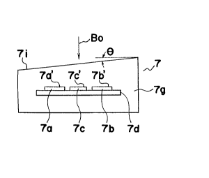
Referring first to Figs. 1 & 2, the photodetector 7
shown therein eomprises a photoeell assembly including a
substrate 7d with photocells 7a, 7b and 7c formed on one
surfaee of the substrate 7d, the photocell assembly being
completely embedded in a transparent resin molded body 7g of
generally cubic configuration. The photocells 7a to 7e have
their respective light reeeiving faces or "windows" 7a',
7b' and 7c' all lying in the same plane, whereas the resin
molded body 7g has a light receiving surface 7i so defined
and so located as to permit the incoming beam BO of light
lZ~i9~L63
g
to travel directly to the windows 7a' to 7c' of the respective
photocells 7a to 7c through such light receiving surface 7i.
-In the prior art, the light receiving surface 7i is planar
and lies parallel to the plane occupied by the photocell
windows 7a' to 7c', as discussed above with reference to
Figs. 8 and 9.
According to the present invention, however, the light
receiving surface 7i is planar, but is inclined at a
predetermined angle ~ to the plane occupied by the photocell
windows 7a' to 7c', said angle ~ being selected to be within
the range of 1.5 to 6 degrees. As a matter of practice, the
plane occupied by the photocell windows 7a' to 7c' assumes a
right-angled relationship with the direction of travel of the
incoming light BO when and so long as the photodetector 7 is
in use.
If the angle ~ is smaller than a minimal limit of 1.5,
the amount of light reflected from the surface 7i towards the
.! photocell windows 7a' to 7c' after having been reflected by the
photocell windows 7a' to 7c', that is, the amount of secondary
reflected light B2, will be large and the interference discussed
above cannot be minimized as much as expected. On the other
i hand, if the angle ~ is greater than a maximum limit of 6,
the incoming light BO will be reflected and/or diffracted in
an increased quantity to such an extent as to result in a
reduced intensity of light falling on the photocell windows
7a' to 7c'.
While in the embodiment shown in Figs 1 and 2 the light
receiving surface 7i is inclined to the plane occupied by
the photocell windows 7a' to 7c', the embodiment shown in
Fig. 3 is such that the photocell assembly is embedded in the
resin molded body 7g in an inclined fashion, so that the
plane occupied by the photocell windows 7a' to 7c' converges
with the light receiving surface 7i at the predetermined
angle ~.
In the embodiment shown in Fig. 4, the light receiving
surface of the resin molded body 7g is so recessed as to
provide an intermediate surface area 7j parallel to the
photocell window 7c', and a pair of side surface areas 7k and
i91~i3
-- 10 --
and 71 defined on respective sides of the surface area 7j in
register with the associated photocell windows 7a' and 7b' and
inclined upwardly therefrom in respective directions away from
each other so as to converge at a predetermined angle ~1 with
a plane parallel to any one of the surface area 7j and the
photocell windows 7a' to 7c'. Alternatively, as shown by the
phantom line in Fig. 4, the light receiving surface of the
resin molded body 7g may be raised outwardly.
Fig. 5 illustrates that, when a photodetector constructed
according to the present invention was used for detecting the
tracking error, the rate of change of the photodetector was
suppressed to a maximum value of 6 to 7% as shown by the
solid line, in contrast to the maximum value of 15 to 20%
exhibited by the prior art photodetector as shown by the
broken line. Fig. 6 illustrates the rates of change exhibited
by samples of photodetectors according to the present invention
(shown by small circles) and those according to the prior art
(shown by x), and it is clear that the former is lower than
the latter. These results are the outcome of the minimized
interference of light as hereinbefore discussed.
` Referring now to Figs. 15 and 16, the light receiving
surface of the resin molded body 7g is covered by a transparent
coating 9 for scattering rays of light reflected by the
photocell windows 7a' to 7c', as indicated by B2 in Fig. 16,
thereby to minimize the secondary reflected light.
The material for the transparent coating 9 will preferably
be a moldable transparent resin of the same quality as the
material for the resin molded body 7g or of a quality capable
of exhibiting excellent adhesion or bonding with the resin
body 7g. Examples of material for the coating 9 include, for
example, an epoxy resin, a UV curable synthetic resin and others.
In order to minimize the loss of light that would occur as the
incoming beam passes through the coating 9, the coating 9
should be as thin as possible, preferably not greater than
100 ~m in thickness. The coating 9 may be formed by any
suitable method, provided that such method is effective to
render one of the opposite surfaces of the coating 9 remote
12~j9163
from the resin molded body 7g roughened, as shown by 9a in
Fig. 16. Such method may include, for example, a spray
-coating method or a painting method that is carried out while
the photodetector is oscillated.
In the embodiment shown in Fig. 17, however, the light
receiving surface 7h of the resin molded body is roughened so
as to have a plurality of alternating hills and dales
extending parallel to each other. This can be readily
accomplished by the use of a mold assembly having a portion
of the mold cavity so patterned as to produce the roughened
light receiving surface 7h.
The surface roughening can also be achieved by providing
the light receiving surface 7h with a plurality of fine
projections 7i as shown in Figs. 18 and 19, or a plurality
f fine recesses. The formation of the fine projections 7i
or the fine recesses can be carried out by a sand blasting
technique, in which case the sand blasting is preferably
followed by a surface treatment such as, for example, an
electropolishing or a chemical surface treatment, because the
sand blasting process lowers the light transmissivity of the
surface 7h. When electropolishing or a chemical surface
treatment is subsequently employed, it should be practiced to
such an extent as to leave surface indentations on the
surface 7h.
A photodetector according to any one of the embodiments
shown in Figs. 15 to 19 has been found to exhibit the same
characteristics as shown and described with reference to Fig.
5.
In the embodiment shown in Figs. 20 and 21, the light
receiving surface 7h is formed with a spherical recess 7m,
50 to 100 ~m in depth and 500 to 800 ~m in diameter, the
diameter being enough to cover all of the photocell windows
7a' to 7c', as best shown in Fig. 21. Instead of the
spherical recess shown in Figs. 20 and 21, a spherical
projection, 50 to 100 ~m in height and S00 to 800 ~m in
diameter, can be formed on the light receiving surface 7h.
An embodiment wherein two spherical recesses 7O are
~2~9163
; .
- 12 -
formed on the light receiving surface 7h in register with the
photocell windows 7a' and 7b' is shown in Figs. 23 and 24.
-Alternatively, spherical projections can be employed in place
of the spherical recesses 7O. In either case, each of the
recesses or projections will preferably have a depth or height
within the range of 50 to 100 ~m and a diameter within the
range of 150 to 170 ~m.
In the embodiments shown in and described with reference
to Figs. 20 and 23, if the depth of the or each spherical
recess, or the height of the or each spherical projection, is
so selected as to have a value greater than 100 ~m with the
curvature reduced, such recess or projection will undesirably
act as a lens obstructing the formation of a beam spot of
effective size on all of the photocell windows or the
associated photocell window.
In the embodiment shown in Fig. 22, a straight groove 7n
is formed in the light receiving surface 7h of the resin
molded body 7g. The direction in which the groove 7n extends
~?' may be either the direction x or the direction y in Fig. 21.
Instead of the groove 7n, a ridge or elongated projection can
be formed on the surface 7h. Two parallel straight grooves
7na and 7nb, or two parallel ridges or elongated projections,
can be formed on the surface 7h to extend in the direction
x in Fig. 24, as shown in Fig. 25.
In the embodiment shown in and described with reference
to Figs. 22 and 25, the depth or height of each groove or
ridge will preferably be within the range of 50 to 100 ~m for
the reason discussed in connection with the embodiments of
Figs. 20 and 23. With respect to the width of the groove or
ridge, it will preferably be within the range of 500 to 800
~m when there is one such as shown in Fig. 22, or within the
range of 150 to 170 ~m each when there are two such as shown
in Fig. 25.
Although the present invention has been fully described
by way of example with reference to the accompanying drawings,
it is to be noted that various changes and modifications will
be apparent to those skilled in the art. In the foregoing
description, reference has been made to the use of a
1~;9~i3
.. . .
- 13 -
photodetector in the three-beam tracking control system.
However, the concept of the present invention is equally
applicable to a one-beam traeking eontrol system wherein the
traeking error signal is detected by a four-segment photocell.