Note: Descriptions are shown in the official language in which they were submitted.
~;'9~ 25307-173
The present invention relates to a packet data communi-
cation system with ring type transmission line represented by
local area network (LAN) and particularly to a high speed, large
capacity packet data communication system for efficiently trans-
mitting various data such as multiplexed voice, moving images and
burst data, etc.
Advancement of hardware/software in the field of
information processing field has been notable recently. With
improvement in processing capability of computers, and micropro-
cessors, high performance and spreading of communication terminals
and work stations, large capacity of files such as optical disks
and diversion of processing with development of diverged data
base, a network is being established between these hardware/soft-
ware and the number of data within the network and between net-
works is increasing.
In addition, an improvement in the function of image
processing hardware/software and the advent of TV conference
systems requires such a network which can handle unified high speed
and large capacity image information in addition to the existing
voice and data.
The background of the invention will be described in
greater detail with reference to the accompanying drawings, in
which:
Figure 1 shows the structure of a Local Area Network;
Figure 2 is a block diagram illustrating the principle
of this invention;
~-~ 3~
25307-173
Figure 3 shows a frame format on a ring type transmission
l1ne;
Figure 4 is a block diagram of an interface node;
Figure 5 is a block diagram of a send interface;
Figure 6 is a block diagram of a receive interface;
Figure 7 is a block diagram of a packet processing
circuit;
Figure 8 is a block diagram of a control circuit;
Figure 9 illustrates a packet sending/receiving sequence
of a system of the present invention;
Figures lO(A) ~ (I) show the process of connecting sending/
receiving buffers to sub-transmission lines;
Figure 11 is a block diagram illustrating another struc-
ture of an interface node; and
Figure 12 shows another frame format of this invention.
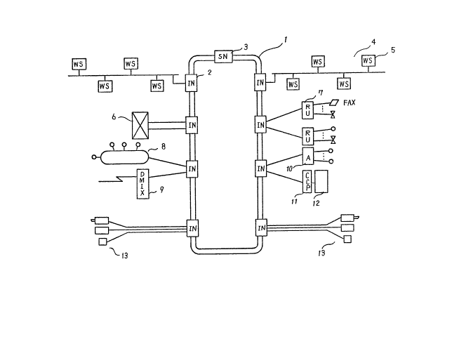
Figure 1 is an example of the structure of a local area
network. A ring type transmission line 1 is employed as a trunk
networ]c. Around the ring type transmission line 1, various inter-
face nodes 2 are provided and each interface node accommodates
various systems. Namely, these are bus type local area network
for communication between a plurality of workstations 5, a digital
PABX 6, telephone sets and facsimiles connected and controlled by
the digital PABX 6, a remote unit 7 which accommodates data
terminals, a low speed ring type local area network 8, communica-
tion control apparatus 11 of a main frame computer 12 and an
adapter 10 which accommodates its TSS terminal, and a TV conference
~9~3~ 25307-173
system 13 and composite multiplexing apparatus 9 for connection
with a high speed leased digital line. Each system is respectively
connected with the high speed ring type network 1 through the
corresponding interface node 2 and system-to-system communication
can be made through the control of such interface node 2. In
addition, the high speed ring type network 1 is supervised by a
supervisor node 3. As an access method to such ring type network
1, a slot ring system is proposed. In this slot ring system, a
plurality of fixed length slots are circulating on the network 1,
each interface node 2 detects the available slot, the data from
the terminals accommodated in a specific node is loaded to the
detected available slot after it is converted to packet data and
then such packet data is sent to the other interface node 2
As a method of realizing a high speed and large capacity
network, it is possible to improve the transmission rate of the
packet i.tself or to transmit in parallel a plurality of packets
without changing the transmission rate of the packet. High speed
operation of LAN has been realized almost by the former method
because it is estimated that the number of gates of control circuit
increases if the latter method is employed. Accordingly, the latter
method has been largely ignored.
However, when considering-the realization of LAN having
a transmission capacity in the order of several hundreds Mb/s,
problems such as high power consumption of the ECL circuit and
difficulty in handling during debug/ maintenance are generated in
the method for improving the transmission rate of the packet. As
3~
25307-173
an effective method for avoiding such problems, the present
inventors have considered employing the parallel communication
system where high speed and large capacity transmission is
realized by transmitting in parallel a plurality of packets and
each packet is processed by a low speed TTL circuit.
It is therefore an object of the present invention to
provide a practical structure of the system for realizing a packet
communication system utilizing such parallel communication system.
It is another object of the present invention to provide
a control method to efficiently transmit a plurality of packets
and receive a plurallty of pa~kets from a plurality of
transmission line in the packet communication system utilizing the
aforementioned parallel communication system.
It is a further object of the present invention to
eli.minate overhead time of communication generated by composite
handling of data in different characteristics such as voice and
burst data and provide a control method for elimination in the
packet communi~ation system utilizing the aforementioned parallel
communication system.
The invention may be summarized as a packet data
communication system, comprislng: a ring-type transmission line
for circulating frames, each frame including a frame header and a
predetermined number of slots in which packets to be transmitted
are loaded, the slots having a predetermined order of priority;
and a plurality of inter~ace nodes, provided on said rlng-type
transmission line, for loading the packets in the slots and for
receiving the packets from the slots, each of said interface nodes
25307-173
including a predetermined number of sub-transmission lines for
passing each of the slots in one of the frames in parallel through
said interface node, terminal interfaces, each having a plurality
of sending buffers for sequentially storing the packets to be
transmitted in a transmission sequence using different ones of the
sending buffers for adjacent packets and a plurality of receiving
buffers for storing the packets to be received, packet processing
means for detecting whether the slots on any of said sub-
transmission lines are available and for detecting the addresses
of the packets in unavailable slots, synchronization means for
synchronizing the frames using information in the frame header and
for supplying a plurality of timing signals to said packet
processing means, switch means for connecting each of the sending
. buffers and the receiving buffers to any one of said sub-
transmission lines, said packet processing means controlling said
switch means -to connect the sending buffer containing a next
packet, as determined by the transmission order, to a
transmissible one of said sub-transmission lines selected in the
predetermined order of priority and containing an available slot,
whereby a group of the packets forming a message may be
transmitted simultaneously from a single interface node, while
maintaining the transmission sequence of the group of the packets.
Reference should now be made to Figures 2 - 10 of the
accompanying drawings and it should be pointed out that throughout
the drawings the same numerals and symbols indicate the same
parts, and the signal lines having the symbol "-~-" indicate that
there actually exist a plurality of signal lines.
~ `q'~ 3~
25307-173
In Figure 2 which illustrates the principle of the
invention, a ring type transmission line 1 is formed by a
plurality of sub-transmission lines S1, S2, S3, S4 having the same
transmission delay time. In this figure, the parallel
transmi~ting of packets is carried out by four sub-transmission
lines S1, S2, S3, S4. The transmission line 1 corresponding to
the main transmission line 1 is formed by a single llne of optical
fiber. Therefore, respective interface nodes 2, 2' are provided
with the series/
5a
~9~
25307-173
parallel conversion c.ircuits 21, 21' and parallel/series conversion
circuits 22, 22' at the input and output sides of the transmission
line 1, bit interleaved four packets on the transmission line 1
are disassembled into respective packets and the disassembled
respective bits are multiplexed in bits. Therefore, the interface
nodes 2, 2' operate as if the four sub-transmission lines Sl, S2,
S3, S4 existed independently.
! 29 is a packet assembling circuit which stores the se-
quence of send data stream (SEND DATA) by assembling the send data
stream flowing into the interface node 2 of the sending side into
the packets; 25, 26, 27, 28 are send buffers which accommodate the
assembled plural packets the sequence of which is stored in the
packet circuit 29; 24 is a switch which stores the sequence of
each packet in the send buffers 25, 26, 27, 28 and transmits the
packets to the transmission lines Sl~ S4 in accordance with the
condition of the sub-transmission lines Sl, S2, S3, S4; 23, 23`
are packet processing circuits which detect the condition of packets
on the sub-transmission lines Sl ~ S4 and control the switch 24; 24'
is a switch which stores said sequence on the sub-transmission
lines Sl ~S4 and transmits the packets to the receive buffers 25',
26', 27', 28' in the same sequence as the accommodation sequence
on the send buffers 25 ~ 28; 29' is a packet disassembling circuit
which reforms the send data stream (SEND DATA) in the sequence in
the receive buffers 25' ~28'.
In Figure 2, the input send data stream (SEND DATA) is
assembled into a plurality of packets in the packet assembling
3~
25307-173
circuit 29 and each packet is accommodated in the send buffers
25 ~28 in such a manner as to store the sequence of the send data
stream. The sequence of the send buffers 25 ~28 is stored by the
switching operation of the switch 24 under the control of packet
processing circuit 23 and the packets are sent to the sub-trans-
mission lines Sl~ S4. The packet processing circuit 23' accommod-
ates the packets in the receive buffers 25'~ 28' in the same
accommodation sequence at the send buffers 25 ~28, keeping the
sequence on the sub-transmission lines Sl~S4. The packet dis-
assembling circuit 29' reconstructs the send data stream in the
sequence on the receiver buffers 25'~ 28'.
The data format on the transmission line 1 is now explain-
ed with reference to Figure 3.
In the abovementioned system, as indicated in Figure 3,
a plurality of Erames consisting of four slots SLOT 1, 2, 3, 4
(accommodating packets) which are multiplexed in parallel by bit
interleave are circulated. In this case, at least four buffers
are required for sending and receiving sides so that four slots
being transmitted in parallel can be accessed simultaneously. The
packets stored in the send buffer are loaded to the slots SLOT 1~4.
Here, ~ the sequential relation between packets on the
send buffers 25~ 28, ~ the sequential relation between packets
on the transmission lines Sl~ S5, and ~ the sequential relation
between packets on the receive buffers 25'~ 28' are defined as
indicated below.
~2-~;9~3~ 25307-173
Sequential relation of packets on the send and receive buffers
In case n send and receive buffers exist, the linear
sequence (number) 1, 2, ..... , n is given to the n buffers (packet
yroup). If the h-th packet accommodated in the buffer g accommodat-
ing packet group is expressed as (g, h), the sequential relation
between two different packets (g, h) and (i, j~ becomes (1) (g, h)
<(i, j) when g < i under the condition that h ~ j or h = j; (2)
(g, h) > (i, j)when g> i under the condition that h >j or h = j.
Namely, a lower number of "row (horizontal)" is superior
between packets of send and receive buffers and a lower number of
"column (vertical)" is superior when the "row" is the same. This
means that the packet having the lower "row" and "column" numbers
for accommodation into the receive buffer is transmitted because
its transmission sequence is considered minimum.
Sequential relation between packets on the transmission_lines
In case m slots to be transmitted on the sub-transmission
lines in parallel exist, the linear sequence numbers 1, 2, ...., n
are given to such slots (SLOT 1, 2, 3, ~, ..., m) as indicated in
Figure 3. If the packet on the i-th slot of the frame passing the
interface node at the time t is expressed as (i, t), the sequence
between two different packets (i, tl) and (j, t2) becomes (1)
(i, tl) < (j, t2) when i< j under the condition that tl< t2 or
tl = t2; or (2) (i, tl) > (j, t2) when i > j under the condition
that tl> t2 or tl t2.
Namely, when the transmission time is different, the
frame with ~uicker transmission time is superior, when the trans-
_ 8
~ ~;9~
25307-173
mission time of the frames is the same, the packet of the slot hav-
ing the lower number is superior. It means that the slots of lower
numbers of quicker frames are set precedingly in case of sending
the packets from the send buffer and the quicker slots and lower
number s]ots are accommodated precedingly in case of accommodating
slots into the receive buffer 7.
~- Next, operations are explained along the transmission
process indicated in Figures lOA ~ I with reference to Figure 2.
This is an example where the 10 packet messages ~
~ are transmitted in parallel with four sub-
transmission lines. As an example, the packet disassembling
circuit 291 partitions the data stream into packets of fixed length
and each buffer is accessed by sending the packets one by one to
the bu~fers 25, 25', 26, 26', 27, 27' , 28 , 28' ,......... The
pac}cets may be transmitted in any sequence if matching is establish-
ed between the packet assembling circuit 29 and the packet dis-
assemblin~ circuit 29'.
Transmission process 1 (Figure lOA):
The packet messages ~ are sequentially accom-
modated in the send buffers 25, 26, 27. In this case, the send
buffer pointer 30 which indicates the buffer storing the packet to
be transmitted next indicates the send buffer 25. Nothing is yet
transmitted to the sub-transmission lines Sl ~S4. The receiver
buffer point 31 indicates the receive buffer 25'. The successive
packets ~ are sequentially
accommodated later as indicated by the parentheses.
~ 25307-173
Transmission process 2 (Figure lOB):
The packet processing circuit 23 detects that the slot
51 of frame 1 and the slot 53 of frame 1 are empty. In case there
are three packets waiting for transmission by the buffer monitor 32
and the send buffer pointer 30 is in the buffer 25, the switch 24
connects the send buffer 25 to the slot 51 and the send buffer 26
to the slot 53. Thereby, the 510t 52 of frame 1 and slot 54 of
frame 1 pass through. Thereby, the stored packets ~ , ~ are
transmitted by giving the readout signal to the send buffers 25
and 26. The send buffer pointer 30 indicates the buffer 27. There-
fore, the pac]cet of the minimum "row" and "column" is extracted
with the first priority and it is then transmitted to the lowest
number slot. The send buffers 25 and 26 accommodate respectively
the successive packets ~ and ~ in place of ~ and ~ .
Such operations are also carried out in the transmission
process 3 (Figure lOC) and 4 (Figure lOD).
Transmission process 5 (Figure lOE):
The packets sent to the sub-transmission lines Sl ~ S4 as
explained previously are then accommodated in the receive buffers
25' ~28' from the sub-transmission lines Sl ~S4. Namely, the pac-
ket processing circuit 23' detects that the packets ~ and ~ of
the frame 1 match the self interface node addresses and the packets
~ and ~ are respectively accommodated in the receive buffers
25' and 26' since the receiver buffer pointer 31 indicates the
receive buffer 25' (Figure lOD). In this case, the switch 24'
switches the slot 51 of frame 1 to the buffer 25' and the slot 53
-- 10
~ 25307-173
of frame 1 to the buffer 26' respectively and sets the receive
buffer pointer 31 to indicate the receive buffer 27' by giving the
write signal to the receive buffers 25', 26'. Therefore, as
explained previously, the packets having younger numbers among
those in the quicker packets are sequentially accommodated in the
sequence of receive buffer number.
Such operations are also carried out in the transmission
processes 6 ~ 9 (Figure 10F ~I). Thereby, packet sending and
receiving come to the end.
The practical structures of interface nodes 2, 2' and
supervisor node 3 are explained with reference to Figure 3 and
Figure 4.
The frame structure of Figure 3 is first explained in
detail.
The packet consisting of header part and information part
is loaded to the slots SLOT 1~ 4 corresponding to a plurality of
sub-transmission lines Sl~ S4. Each packet is multiplexed by bit
interleave and is loaded to the packet part in the frame of trans-
mission line 1. The frame header is added to the heading part of
packet in the frame. This frame header is provided with the frame
synchronization pattern for deciding each bit position of frame,
frame counter which is intrinsic to one frame (discriminated from
the other frame circulating on the same transmission line) and the
region for loading the command transmitted between the interface
node and the supervisor node for reserving the slots for the
synchronizing communication, or sent from the console connected to
~9~
25307-173
the supervisor node 3 at the time of initial start of system or
during the test. Meanwhile, the heading part of the packet is pro-
vided with the packet header being divided into four fields of
control field CTL, receive address field RA, send address SA and
data administration field ~M. Moreover, the control field CTL is
composed of a packet valid/invalid indication flag AV, reserved/
not-reserved indication flat CMl, a flag CM2 which indicates that
the data in the information par-t is the burst information, a flag
PS which indicates that the packet is not received because the
terminal interface 40 is busy and a flag ER which designated whether
the flag AV is deleted by the send node or receive node.
Moreover, the trailing part of the packet is provided
with a check bi-t for detecting and correcting errors in the packet,
such check bit being provided at the trailing part of the frame as in
the case of each packet. The function of the packet header will
be explained later.
Figure 4 is a block diagram of the internal structure
of the interface nodes 2, 2' and supervisor node 3.
The optical fiber 1 corresponds to the main transmission
line 1 in Figure 1 and the frame having the structure consis-ting
of a plurality of slots SLOT 1 ~4 indicated in Figure 3 circulates
therein. A photoelectric converter 30 converts the received
optical signal into an electric signal and then inputs said receiv-
ed signal after waveform shaping to a frame synchronizing circuit
34 and serial/parallel conversion circuit 32. The frame synchroniz-
ing circuit 34 detects the frame synchronizing pattern added to
L~3~3
25307-173
the heading part of frame for frame synchronization and outputs
various timing signals for deciding bit position of the frame to
packet processing circuits 35, 36, 37, 38, a control circuit 39 and
the serial/parallel converting circuit 32. The serial/parallel
converting circuit 32 is driven by a clock signal synchronized with
the frame on the -transmission line 1 input from the frame synchro-
nizing circuit 34 and outputs a parallel signal of 4 bits. This
parallel signal is the packet loaded on each slot SLOT 1 ~4 in
Figure 3.
The packet processing circuits 35 ~38 analyze the packet
header on the basis of the timing signal from the frame synchro-
nizing circuit 34. The results of analysis of packet processing
circuits 35 ~38 are sent to the control circuit 39 through CONT
BUSB. The control circuit 39 changes switches 44 ~47 based on the
result of analysis and thereby sends the packets stored in the
send buffers 25 ~28 existing in the send interface 42 (Figure 5)
within the terminal interface 40 to the parallel/serial converting
circuit 33 through the send data bus and then executes the control
for sending it to the transmission line 1 and to store the received
packets to the receive buffers 25'~ 28' existing in the receive
interface 41 tFigure G) through the receive data bus. These con-
trols are executed by the control signal transmitted through the
CONT BUSA. The terminal interface 40 is provided with the send
interface 42 consisting of the switch 24, send buffers 25 ~ 28 and
packet assembling circuit 29 indicated in Figure 2 and the receive
interface 41 consisting of the switch 24', receive buffers 25'~ 28'
b~
25307-173
and packet disassembling eireuit 29'. Figure 4 indicates only one
unit of terminal interface 40 but a plurality of untis may be
conneeted.
The eontrol cireuit 39 deeides the transmission mode
(synehronous eontinuous eommunication or burst communication) de-
pending on the send request from the terminal connected to the
terminal interface 40. When synehronous eontinuous communieation
is deeided, a necessary number of slots are reserved, in aeeordanee
with the amount of information, to the supervisor node 3 using the
paeket header indicated in Figure 3 by controlling the packet
processing cireuits 35 ~38.
Here, since the phase of the parallel slots is the same
in the frame strueture indicated in Figure 3, the packet headers
reach the packet proeessing eircuit simultaneously. Therefore,
the packet proeessing cireuits in the same number as the parallel
slots must be prepared.
In this ease, a frame strueture sueh that the phases of
slots transEerred in bit multiplex to the ring type network are
deviated for the speeified amount as indiea-ted in Figure 2 is em-
ployed. The E of #2 slot~ #N slot indieates the dummy region in
the same length as the frame header for time differenee adjustment
and the frame header is not provided up to the ~2 ~#N slots.
The strueture of Figure 4 is therefore ehanged into Figure 11 and
outputs Sl~ S4 of the serial/parallel eonverting eireuit 32 are
respeetively input to the seleetor 52 through the delay circuits
48 ~51. Since the frame synchronizing circuit 34 is capable of
detecting the packet header of eaeh packet, the paeket header
- 14 -
~~,9~
25307-173
detection signal sent from the frame synchronizing circuit 34 is
input to the selector 52 and only one of said outputs Sl~ S4 is
input to the packer processing circuit 38 on the time division
basis.
The output to the receive data bus from the packet pro-
cessing circuit 38 is also provided through the selector 54 on the
time division basis.
The output to the switches 44 ~47 can also be provided
by the selector 53 on the time division basis.
The switch timing signals of selectors 52 ~54 can be
generated in the frame synchronizing circuit 34. With such struc-
ture, only one packet processing circuit is necessary and thereby
the hardware can be saved.
The delay circuits 48 ~51 are provided for queuing the
delay in operation of -the packet processing circuit. As described
previously, the packet communication system with ring type trans-
mission line of the present invention is required to cope flexible
with the system where communication (synchronous continuous com-
munication) which is required to have periodicity in data transfer
like image communication or voice communication and communication
(burst communication) which is not required to guarantee the
periodicity of data transfer unlike the data communication between
computers but is required to reduce the transmission delay as much
as possible coexist and the communication mode changes dynamically.
However, the slot ring system, where the empty slots
(available slots) among the slots defined by dividing the frame
3~
25307-173
circulated through the ring type transmission line for the speci-
fied length are sei2ed and data transmission between the terminals
connected to the ring type transmission line by loading the
packets to such slots, must inevitably wait temporarily for trans-
mission of data because if data transmission request, namely many
requests for use of empty slots are generated at a time, the
empty slots becomes short for re~uest of use. Under such condi-
tiOII, the synchronous continuous communication which is restricted
in the transfer periodicity will result in serious interference
such as data overflow or data underflow, etc.
In general, therefore, as a means for eliminating such
disadvantage, the packets of the specified nllmber which are cir-
culated through the loop type transmission line are sorted into
two kinds, one which is packets for synchronous continuous communi-
cation and the other is packets for burst communication. For
the former kind of packets, a number of communications is always
set to a value less than the number of packets and the system
design is defined considering that packets can be used any time
desired for communication.
However, this system provides a problem that flexibility
is insufficient because the ratio between the synchronous continu-
ous communication and burst communication is fixed and flexible
measures for the system where the communication mode changes
dynamically is difficult.
Therefore, the packet communication system of the pre-
sent invention assigns the packet numbers to the packets by pro-
- 16
~9~
25~07-173
viding the reserved information part to the specified region of
packet. Moreover, the particular supervisor node 3 supervises
assignment of reserved packets, notification of packet numbers and
reserved assignment condition of packets, while ordinary interface
node 2 reserves the packets having the numbers assigned to the self
interface node and executes the packet send when the empty reserved
packet arrives after reservation.
Namely, in the packet management by the supervisor node
3, reservation of packets can be made variably when required so
long as the sum of the number of packets being used and to be used
does not exceed the total number of packets and thereby the packet
management assures flexible measures for the communication system
where the synchronous continuous communication and burst communi-
cation coexist.
To explain in detail the procedures for data transmission
and reception, the structure of each part of Figure 4 will now be
explained in detail.
Send interface 42 (Figure 5):
As explained previously, the interface node 2 is provided
with a plurality of terminal interfaces 40 and respective terminal
interfaces are connected with terminals in different communication
modes. Accordingly, prior to transmission, the terminal sets the
signal which indicates the transmission mode (synchronous con-
tinuous communication or burst communication) to the register 61 in
the send interface 42. Simultaneously, in case the send mode is
the synchronous continuous communication, the terminal also sets
~9L~ 25307-173
the receive terminal address and amount of send data to the
register 61. Upon setting the send request to the register 61,
the terminal sends the send data and receive address to the packet
assembling circuit 29. The packet assembling circuit 29 adds the
header part and check bit to the send data and assembles the
packet in the specified length as indicated in Figure 3. In this
case, the receive address is set to the field RA in the packet
header, while the interface node address to which the packet itself
belongs and the address of terminal connected are set to the field
SA. Each flag of CTL field is controlled by the packet processing
circuits 35~ 38.
The packets sequentially assembled in the sequence of the
input data stream in the packet assembling circuit 29 are sequen-
tially stored in the send buffers 25, 26, 27, 28, 25, ..... , 26, 27,
28, in accordance with said sequential relation.definition of
packets.
In this case, the address of buffer for storing is de-
signated by sequentially counting up the write address counter 59.
The send buffers 25 ~28 temporarily store the packets to be input
from the packet assembling circuit 29 and the output side of buffers
25~ 28 can be connected with any send data bus through the switch
24. The buffer monitor 32 monitors a number of packets stored in
the send buffers 25~ 28 and notifies the result of monitoring to
the control par-t 39 through the CONT BUSA. The buffer pointer 30
designates one buffer in which the packet to be read next is stored.
The selection and control part 52 decodes the send packet indication
~ 18 -
3~
25307-173
signal input from the control part 39 through the CONT BUSA and a
designated value of buffer pointer 30 to control the connection
between the buffers 25 ~28 and send data buses Sl ~S4 by changing
over the switch 24 and gives the readout instruction to the buffer
in which the packets to be sent are stored.
Receive interface 41 (Figure 6):
The structure of receive interface 41 is similar to that
of the send interface 42 indicated in Figure 5 and therefore only
the differences will be explained hereunder.
The input side of the receive buffers 25'~ 28' can be
connected with any receive data buffer through the switch 24'.
Moreover, the buffer monitor 32 monitors a number of packets stored
in the receive buffers 25'~ 28'. The buffer pointer 31 designates
the buffer for storing the packets to be received next. The
selection and control circuit 63 decodes the receive packet in-
dication signa], sent from the control part 39 and content of
bufEer pointer 31, makes switching control of the switch 24 and
then sends the write indication signal to the buffer to which the
received packets are stored. As in the case of write address coun-
ter 59 indicated in Figure 5, the read address counter 71 sequen-
tially designates the buffers to read the packets like the receiver
buffers 25', 26', 27', 28', 25' .... 27', 28'. In the above
explanation, four send/receive buffers are provided to four parallel
transmission lines Sl, S2, S3, S4, but it is not always required
that the number of parallel transmission lines corresponds to
the number of buffers on a one to one basis and there is no such
-- 19 --
~~9~
25307-173
correspondence by providing a switch between the transmission line
and buffers because each buffer can be connected to any trans-
mission line Sl ~S4.
Packet processing circuits 35, 36, 37, 38 (Figure 7):
Figure 7 indicates the structure of the packet processiny
circuit. Since the packet processing circuits are all identical,
the structure of only one circuit is indicated. The timing signal
which is sent to each part for deciding the bit position of the
received packet from the frame synchronization circuit 34 is
eliminated here for simplification.
The packets on the SLOTs 1~ 4 (Figure 3) of the transmis-
sion lines Sl~ S4 are input to the shift register 72. The shift
register 72 is driven by the timing signal synchronized with the
received packets and when these packets are all input, the contents
of control field CTL are input to the control field decoder 74, the
contents of receive address field RA are input to the receive
address comparison circuit 75, and the contents of send address
field are input to the send address comparison circuit 76. The
address of interface node 2 and address of each terminal to be
accommodated to the interface node 2 are previously set to the
register 77 by PMV 43 through the CONT BUSB.
The control field decoder 74 displays the condition of
received packets in accordance with the following table by decoding
the contents of the control field CTN.
- 20 -
~9~3~
25307-173
~ .. .
AV (valid/invalid indication unused Packet Packet beinq used
.. ._. ,
CMl (reserva-tion indication unreserved reserved synchronous
flag) _ ~_ - - - - packet _ continuous packet
CM2 (burst communication Burst communication
indication flag) _ ~ packet
PS (packet receiving con- Receive buffer busy
dition indication flag) (not received)
~ . .
ER (AV elimination node elimination of elimination of send
indication flag) receive station station
The receive address comparison circuit 75 compares the
address of RA field of received packet and the address being set
to the register 77, detects whether or not the received packet has
as a destination its own interface node with reference to the out-
put of the con-trol field decoder 74 and also detects -the terminal
address being accommodated in i-ts own interface node. When the
receive addresses have ma-tched, the receive address match signal
BRSELn is sent together wi-th -the terminal address.
The send address comparison circuit 76 compares the
address of SA Eield of the received packe-t and -the address being
se-t to the register 77 and de-tects whether or not the packe-t is
transmitted from own interface node with reference to the output
of the control field decoder 74.
All bits of the received packets are input to the check
circuit 73 and parity check is carried out.
The control signal generating circuit 79 generates the
following control signals in accordance with the decoding result
of control field decoder 74, comparison result of receive address
'9 L~3 ~
25307-173
comparison circuit 75, comparison result of send address comparison
circuit 76 and receive buffer busy signal from the control circuit
39 (RBBSYk). n is the slot number dealt with the packet processing
circuit.
Received slot available (AVAILn)
When the slot is unused:
The packet to its own interface node is received without
error and the AV flag can be deleted in the receive station
When the packet sent from its own node is received after
circulation (when end of reception of each node is decided at the
own station during communication to a plurality of nodes)
Setting of each flag of control field CTL (SETFRn)
Indication of synchronous continuous slot (SYNCn)
~emote station receive buffer busy (BSYn)
The packets sent from the own node are not received due
to the remote station receive busy state.
The SETFRn among above signals is input to the packet
header renewal circuit 78 to set the valid/invalid indication flag
AV in the control Eield CTL of the header of receive packet to be
input in the same way and reservation indication bit CMl.
With the SELECT signal from the control circuit 39,
the switching control of the selection circuit 147 is carried out
so that the packet from the header renewal circuit 78 is allowed
to pass through the selection circuit 147 or the data from the
header renewal circuit 78 is used only for the control field
of the header and the packets on the send data bus are
output for the other part, and thereby the packets are
output to the transmission lines Sl~ S4.
Control circuit CONT 39 (Fig. 8):
Since the control circuit CONT 39 is provided in
common for the packet processing circuits 35^v38 and a
plurality of terminal interfaces 40, a plurality of
control signals are also used to/from respective
portions. But in Fig. 8, such control siqnal is
simplified. The receivable packets are input to the
receive packet control circuit 80 from the buffer
monitor 33 of each receive interface 41 through CONT
BUSA and the receive address coincidence signal RBSELn
(including terminal address) is also input thereto from
the packet processing circuit. The received packet
control circuit 80 refers two control signals input and
judges whether these can be received or not. ~hen
these are receivable, the slot number based on RBSELn
is informed to the terminal interface 40 based on the
receive address. If receive buffer is shortage, the
receive buffer busy signal (RBBSY) is issued to the
corresponding packet processing circuit.
The terminal send request analysis circuit 82
reads the register 61 within each send interface 42
with a constan. pe iod. The co~munication mode and a
- 23 -
~&9~-3~
number of requested slots are set to the register 61.
Therefore, the terminal send request analysis circuit
82 inputs a number of send requests and a number of
requested slots of synchronous continuous communicat-
ions to the synchronous continuous communication
management circuit 83 and moreover a number of send
requests and a number or requested slots of the burst
communication to the burst communication management
circuit 85.
The allocated slot management circuit 81 is pro-
vided with a table for storing the frame counter given
to each terminal interface for the synchronous continu-
ous communication and the slot numbers (SLOTl, 2, 3, 4)
in the frame. When the frame header is input to the
frame synchronous circuit 34, the frame synchronous
circuit 34 detects the frame counter and said
frame is input to the allocated slot management circuit
81. With this frame counter used as the address, the
allocated slot management circuit 81 reads that the
j~th slot is allocated to the ]~-th terminal interface
from the table and notifies it to the synchronous
continuous communication management circuit 83.
Renewal of table content (renewal of allocated
frame, slot information) is executed by MPU 43 througn
- 24 -
CONT BUSA and MPU43 reads table content and confirms
the allocated frame and slot information.
The synchronous continuous communication manage-
ment circuit 83 generates the send select signal for
the synchronous continuous communication from the
inputs sent from the terminal send request analysis
circuit 82 and allocated slot management circuit 81 and
AVAILn and SYNCn from the pac.~et processlng circuits 35
38.
Namely, when AVAILn and SYNCn are input from the
pac.~et processing circuit corresponding to the n-th
slot, the allocated slot number and receive slot match
and these are available, indicating that the terminal
which has reserved -the slot n in the table can be used
for the synchronous continuous communication.
t Therefore the send select signal is transmitted to the
terminal interface which accommodates the reserved
terminal. This send select signal is input to the
select control circuit 52 of the send interface through
the CONT BUSA.
The burst communication management circuit 85 sets
the terminal interfaces with priority 1 ~ m for the
burst communication depending on the information sent
from the terminal send request analysis ci-cui. 82 and
- 25 -
-
34~3~
inputs the burst data to the burst data selection
control circuit 86.
The available slot analysis circuit 84 judges how
many slots is avaialble for the burst communication
from the AVAILn and SYNCHn signals and then inputs the
signals to the burst data selection control circuit 86.
Namely, when only AVAILn is input (SYNCHn is not
input), the n-th slot is not reserved and it can be
allocated for the burst communication.
The burst data selection and control circuit 86
allocates the available slots sequentially from the
terminal interface having a higher order depending on
the determined priority sequence and then outputs the
send select signal for the burst communication. The
select signals for synchronous continuous commùnicat-
ion and burst communication are input to the send
packet control circuit 2 and the send select signal for
controlling the selection circuit ~7 in the packet
processing circuit and the send select signal input to
the selection control circuit 52 in the send interface
are output.
The register 87 holds the terminal interface of
the lowest priority among the terminal interfaces to
which the slots are allocated in the burst data
-- 26 --
3~
selection and control circuit 86 and then determines
the terminal interface with highest priority in the
next frame.
Res?ective circuits have been explained previously
in detail and the pac.lcet send sequence is then
explained wit.h reference to Fig. 9.
~ For the reservation for svnchronous continu-
ous communication by the terminal accommodated to the
terminal interface 40, the send mode (the mode is the
same as burst communication in the case of
reservation), receive address and a number of packets
required for transmicsion are set first to the register
61.
~ The send data is input to the packet
assembling circuit 29 in order to form a packet and it
is then stored in the send buffers 25 ~ 28. In this
case, the receive address RA in the packet header is
the supervisor node and moreover the receive address
and a number of paclcets required actually and data
which indicates reservation request for the synchro-
nous continuous communication exist within the
information region of pacXet.
~ The control circuit 39 recognizes the send
mode. Because of the burst communicalion, the priority
- 27 -
9 L~
sequence explained for Fig. 8 is given to the relevant
terminal interface. The specified empty slot is seized
depending on such priority sequence and the packet in
the send buffer is received by the supervisor node.
~ The supervisor node is also provided with the
structure as indicated in Fig. 4 like other interface
node and the allocated slot management circuit 81 of -
the control circuit 39 is also provided with tables for
all nodes. In addition, MPU is` accommodated in the
terminal interface within the supervisor node. There-
fore, information of pac.'cet destinated to own node is
notified to CPU through the terminal interface. CPU
makes reference to the table of allocated slot
management circuit 81 of the control circuit 39 and
checks whether the actual party for communication of
the relevant terminal has already reserved the pacXet
or not. When the communication party does not yet
reserve the pac]cet, leaving the requested number of
pac~cets unreserved, the table is renewed, the relevant
terminal is reserved and registered, end of reservation
is notified to the relevant terminal with the ordinary
burst communication and the packet number allocate~ by
reservation, frame number and slot number are als_
notified. When the other par J has already rese~-~ed
- 28 -
~ 9 L~ 3 ~
the packet or the reserved number of packets are not
available, reservation disable signal is sent to the
relevant terminal.
~ The relevant terminal which has received the
end of reservation requests renewal of table to MPU.
The slot number and relevant terminal address are
stored to the table with the allocated frame number
used as the address.
~ Data is set to the register 61 depending on
the synchronous continuous communication request of the
relevant terminal. Upon decision of synchronous
continuous communication, the control circuit 39 turns
on the reservation indication flag of packet header of
the packet of a slot number after the relevant terminal
address and such slot number are read from the table
with the frame number used as the address. The control
circuit waits until the valid/invalid indication flag
of packet of this slot indicates invalid condition.
~ When it is detected that the valid/invalid
indication flag indicates invalid condition, the packet
stored in the send buffer is transmitted. In this
case, the header is updated so that the valid/invalid
indication flag indicates the valid condition.
In the case of ordinary burst communication
- 29 -
3~
which does not set reservation, the packet is sent with
the receive address considered as the ordinary terminal
as in the case of step 3 .
~ The interface node which has received this
packet sends this packet to the receive terminal and
checks whether there are send data from the terminal in
the own node.
~ In case there is no send data, the valid/
invalid indication flag indicates the invalid condition
and the received packet is directly sent.
~ In case there is send data, it is checked
whether such send data is reserved or not. In case
this data is reserved , the processing same as that in
the step 10 is carried out.
~ In case such send data is not reserved, the
valid/invalid indication flag of received packet
indicates the valid condition and data is transmitted.
- 30 -
~i9~
25307-173
According to the above method, in order to perform the
communication between the interface node and the supervisory node
for sending the request of reserving the slots from the interface
node or for informing the interface node the allowance of reserva-
tion and the reserved slot number from the supervisory node, it
is necessary to access the empty slots so that it is required to
wait until the empty slots are indicated.
So, as described with Eigure 3, it is efficient to use
the field for the command of frame header. Namely, the field is
allocated to the interface nodes and the supervisory node for the
management of the network, so that this field is not used as many
as the slots.
Then, describing the structure to perform above method
with reference to Figure 4. O/E 30 outputs the frame of Figure 3
to the frame header processing circuit 148. The frame header
processing circuit 148 is driven by the timing signals from the
frame synchronizing circuit 34 and is set the field of command
(command field) of frame header at the shift register 1. The con-
tents of the command field are decoded at the frame header proces-
sing circuit 148 and output the decoded signal to the CONT 39 via
CONT BUSB.
When the request of reservation of the slots are sent to
the CONT 39, CONT 39 is gating the output corresponding to the
command field from the shift register 1 and, on behalf of the
gating output of the shift register l, CONT 39 is set the command
for reservation to the shift register 2. Then, the shift register
- 31 -
9~3~3
25307-173
2 output the up-to-date frame header in series to the switch 50
in accordance with the timing signal from the frame synchronizing
circuit.
At this time, switch 50 select the output of the frame
header processing circuit 148.
After output from the frame header processing circuit
148 ends, the switch 50 immediately select the output from P/S
converter 33 so that the frame header is added to the packet
header and the frame is completely reconstructed.