Note: Descriptions are shown in the official language in which they were submitted.
Il lZ6971~} ~
~ 5~ M~EM SY6~EM ~VINa I~BOV~D D~O~UL,A~'IO~ ~LIABILITY
1 ~9
1 Fl~ld of the Inv~ntlon
l This ih~ent~On relates to a modem system, ~n~ n~re
¦ particularly t~ ~ mod~m ~yst~m in whi~h, on th~ ~ignal transmit-
¦ ting slde, dig~tal data 8~e ~ubj~cted to PSK (ph~s~ s~ift keying)
¦ modulatlon~ while, on the signAI reee~vinE side~ a delay modulR-
¦ tion is carried out to obtain th~ originAl di~ital data.
1 2 Brie~ Di~cussion o~ the Art
I ~
¦ In one ex~mple of ~ con~entional di~ltal slgnAl trans-
¦ mitt~ng system, a di~it~ n~l is PSK-mo~ulated on th~ slgn~l
tr~n~mitting side, while the 6i~nal 1~ dem~d~lleted to obtain the
original digit~ n~l on the s~gn~l re~2iving side.
In s~ch a PSK modulatlon ~y~tem, d~glt~l ~ignsls "0~
l and ~1~ are transmltted on the varlation In ph~se o~ t~ carrier
¦ W~V2, and: the C¦N deterio~ati~n ~s minlmi~ed, Th~t is, ~hæ P~K
mooUla~lOn sy~tem ~8 excellent signsl ch~rac~erl&tics and has
ccordingly bssn extænslvely ~nployed for tr~nsmissIon o~ digital
sIgn~ls,
.
:'''
' ` .
~ ~;9~
Objects~ Eeature.q nnd advantacle3 oE tl
.invant.ion w.ilL be betker undarstoo(l ~rom t.lle Eollowir
detailed descr:ipt.ion which :is provided :in connection witl
the accompanying draw.ings.
Figures ltA), 1(~), l(C) and l(D) are s.ignal
diagrams useful in describing one example of a modulation
system of the invention;
Figures 2(A), 2(B), 2(C), 2(D), 2(E), 2(F), 2(G)
and 2(H) are signal aiagrams useful in describing one
example of a demodulation system of the invention;
~26~
2b
Figure. 3 is all el~ctrical circ~lit s~lowi.n(l one
exampl~ oE a demodu:Lat:ion circ~uit usecl in t:lle inVelll".iOIl;
Figures ~ (B), ~(C), ~(I)) nnd ~(fi') a
55(A), 5(B), S(C), S(D) and 5(E) are signal. d:iacJrams usoE
in describing other e~ampl.es oE a democlulation system;
Figure 6 .i9 an electrlcal circu:it showing
another example of a demodulation circuit used in the
invantion;
lOFigures 7(~), 7(B) and 7(C) are signal diagrams
useful in exp].aining the operation of the demodulation
circuit of Figure 6;
Figure 8(A) is a block diagram of a conventional
delay detector;
15Figure 8(B) is a circuit diagram of the phase
comparator shown in Figuxe 8(A);
Figure 8(C) is a signal diagram useful in
explaining the operation of the Figure 8(B) circuit;
Figures 9(A), 9(B), 9(C), 9(D), and 9(E) are
20signal diagrams useful in explaining the operation of the
delay detector of Figure 8(A);
Figures lO and ll are respective signal diagrams
useful in explaining the operation of conventional
modulation systems;
25Figure 12 is a circuit diagram of a modulation
circuit which may be used in the invention;
Figure 13 is a signal diagram useful in
explaining operation of the Figure 12 circuit; and
Figure 14 is a phase shift circuit used in
30conjunction with the Figure 12 modulation circuit.
.,
2c
The PSK modulation system is oEterl coll~L~Iure(l;l;
a so-called "MSI~ system" or a so-called "I)S[~ sysl:elrl".
In the MSK syst:em, as shown in F'i~Jure lO, W~
the signal is in the "mark" state, the phase is increased
linearly hy 180 for a time slot period oE the signal; and
when the signal is in "space" state, the phase is
decreased linearly by 180 for a time slot period of the
signal.
In the DSR system, as shown in Figure 11, when
the signal is in "mark" state, a time slot period of the
signal is divided into two parts so -that the phase is
increased in two steps; and when the signal is in "space"
state, a time slot period of the signal is divided into
two parts so that the phase is decreased in two steps.
In the MSK system, the phase changes
continuously. Therefore, the MSK system is advantageous
in that the occupied frequency band-width is small. On
the other hand, the DSK system is advantageous in that it
is substantially not affected by multi-path fading and is
therefore suitable for wide-band data transmission.
In order to demodulate a signal which is PSK-
modulated, a delay detection system or a synchronous
detection system are generally employed.
In the delay detection system, a signal received
is divided into two parts. One of the two parts, after
being delayed by one (1) or half (1/2) signal period of
the modulation by a delay circuit, is supplied to a phase
comparator, while the other is applied, as it is, to the
phase comparator, so that the
9 7 ~ ~
P~-modul~te~ signal ls d~no~u1ated; I.~., th~ orlKIn~l di~itnl
Si~nAI i9 obtn;ned. Thts wtll now bc do9cribod In more dQtnll.
It is ~s~umed th~t, In a del~y d~t~at)on devIce ~hO~h In PI~.
8~), it9 input voltage Yin Is cos ( Q t ~ ~ (t)~ wh~r~ Q i~ the
angular fr~qu~n~y o~ th~ c~r~ier, t i5 th~ time ~nd ~ (t) is the
ph~çe modulation ~unotion. ~he input ~olta~ Yin i~ diYided into
~wo parts. One of th~ t~o p~rt~ is supplled to ~ termlnal o~
phase oompArator ~, while the other is app}ie~ to Another term-
~nsl o~ the phase ~omp~rator 22 ~fter being ~e1ayed by ~ prede-
termlned period o~ time TR by a del~y circui~ 21. The one of the
t~o parts, n~ely, ~ signal Yc i~
Yc = Yi n = cos ( ~ t + ~ ~t)), ~nd
the other, namely a signa1 Yd iS!
Yd = co~ ~ n ( t ~ TR) ~ ~ ~t - TR))
If, in this oonnectlon, th~ phase comp~rator ~ is
arranged as sho~m in Fig. 8~B~ ~o th~t the output is proportional
to ~h~ phase di~erence as indicated in Pig. 8 (C) ~ then the phas~
difference ~8 ls~ - .
Q~ - n TR + 9 ~t) ~ ~ (t ~ TR)
In the above expre~sion, it ~s ~ssentl~l ~ha~, in the
MæK system ~r rSK system, the delay tim~ T~ is determined as
tollows~ ~r/2 (whera T i~ one (1) time slot o~ th~ signBl).
. Ii ~ TR - tan-l3 ~ or .Q .= ..~ /TR = (~n~ /T, ~hen
the ~e~er~nce polnt of the pha~e eomp~r1son can be set at ths
center ~ the rsnge o~ op~ration o~ th~ phase comp~rator.
By way of example, the c~se of ths DSK sy~t~m wI11 b~
~escr~bed. However, ~t should b~ noted th~t the following de-
scrlption is ~ppl~aable to t~e case of the M~K syst~m in the same
manner.
ii 1;~1697~l~
~Yhnn ~ ~t) ~ ~ ( t - TK) ~ 0~
~a - ~ T~ a (2n~
Th~re~ore, t~ll5 p~int i~ the ph~e ro~ ncc point In th~ ~nso
wh~ th~re ;~ no ph~e ~hi~t~ ~nd ~n o~tput ~orr~spollding ~o the
point which is shl~ted by ~ ~t) - ~ ~t ~ rom the referenc~
point is obt~ined.
1n the ~s~ o~ a msrk-æ,pace ~i~n~l, its ph~s~ function
a ~t~ ls ~3 ghown In ~ig. 9~A), and ~ (t - T/2) in F~g. 9(13).
- 'rher~fDre, ~s ~hown in Fig. 9(C:), a (t~ t - T/2)
~ or a "m~rk" period, ~nd - It /2 ~or a "sp~c~" period.
Thus~ ~n output waveform ~s show~ in ~i~. 9~ obtalned
accordlng to ~n output chAra~teri~tic as shown in Fi~. 9~D).
That i~;3 an output obtained i~ 3Yo/4 ~or ~ "m~rk" per~oS3, and
Yol4 ~or & "space" period~
Accord~ngly, it ~n be t3et~rmin~d th~t the s~na1 i~ in
a "m~rk" ~tate when the output ~ the phase comp~ or 22 exceeds
Vo/27 snd it is in ~ "space~ gtste when the output i~ VG~a or
lower .
Thus f~ ~ del~y detection s~heme hAs ~een des~ribed~
Now a syn~hronQus det~ction schem~ w~ll be deseribed. In the
synchronous detection cir¢uitS ~ 51gn~1 r~ceived ~ div~ded into
two p~rts, whioh ~re ~pp1ied to phRse comp~ralto~s, respectivelg,
and the outpu~ gn~ hose frequency ~s eq~lal to ~he carrier .-
~re9uency o~ the ~ignal rece~v~d) o~ a Yoltage~controlled oscil-
lator in 9 ph~ge syT~chronlz~t~oT~ loop is ~uppl ied to one of thephs~e ~ompat~tors wh~le the output sS~nal, after b~ing phase-
3hi~ted by 90, is ~pplied to the other phase comp~ra~or, so ~hat
-- 4 --
.
.
'':.
th~ originAl d~g~t~l gi~n~l is obtatnccl acuorcllng to th~ outputslgnAls o~ th~ two ph~s~ compar~to~s ~f, ~l~r~lr~ rF~c~ ),ln,
vo l ~ l 4 - s, No . :L O, 19 ~ C~3 K Mo tl ll l A t i o n
Sy~tem Tr~nsn~s~on Ch~racteri~tlc~ by K~zu~ki Mu~ot~, ~nd
Kenklchi ~lP~ide).
A~ desoribe~ aboYe, in the cagb wher~ the PSK-m~dul~ted
s~gnal is ~emodulated by the ~el~y detectl~n system, the slgnal
receiYed is d~ dad into two p~rts, and only one o~ the t~o pRr'Ls
i5 del~ye~. Therefor2, the method ~s adYant~geous in th~t the
circu;try is simp1e; however~ it ~s di~dvantageou~ in thse, in
the case of ~ high ~requency band digi tal signal trsn~mi~sion,
the demodulation rel~bility Ss low. Thl~ w;ll ~ç described ~n
more ~etall. In the dela~ ~etection ~yste3n, the oper~tin~ refer-
ence po~nt ls ~8 - 5? T/2. Th~ra~ore~ When the c~rrier an~u-
lar ~equ~ncy changes by ~ a, for ingt~ce, be~us~ of a tem-
perature Yari2t~on~ then the oper~tlng re~erence polnt Is Rl~o
shi~ted ~s much a3 ~ ~ T/2, ~ thi~ c~lan3~e i3 gre~ hen ~he
~m~rX" ~nd ~sp~c6~t c~nnot ~e determ~ned ~ccord~ng ~o whether or
not the output lev~l of the phase compar~tor axce~ds Vo/2, ~or
in~tan~e, when the carr~er frequenoy ls l.S GHz and the eoeffic-
ient o~ ~ariation with t~mperAture of the os~illator ls 10 6,
then th~ ~requency YsriR~iOn ls IB KHæ. I~., in th~ case, the
. data ~r~n3mi~io~ ~pee~ i~ 3e~ ~o 32 Kbps, then T-1/32 mseo, ~nd
a T/2 a 0.469 ~; Sh~t is, the shi~t ~f the op~ratin~ r~er-
ena~ point is ~bst~ntially ~ 1~. In pra~t~ce~ the operatin~
re~r~nos point i9 ~l~o a~ected b~ noise snd intererence wave~
by multipath in addit~on to ~e~p~ature v~riation~ ~nd is t~us even
- 5 -
~ .
~urthar shl~ted. Ther~fo~e, it 1~ oft~n diftlcult ~o ~eterrninc,
by oompdrlng the output level o~ th~ phQ3c oompnrntor wi th th~
pr~etermine~1 re~rence 1~Ye1, whather thR ~ in "mtlrk~
~t~t~ or in ~p~ce" ~t~te.
~ ~ynchronou~ fl~te~tion 3y~tem i~ bn~ed on th~ repro-
duction o~ 8 o~rri~r fr~qu~cy by ~ CostQs loop. rherefore, the
synchronous dete~tlon sygtem, unllke the phase detection ~y~temt
i~ free .~r~1 problems ~ttibute~ to A frequen~y yari~tiDn~ thus
perm~tting si~nal demodul~tion with hlgh ac~ur~y. ~owever, th~
synchronous dete~t~on sy~tem h~ its own limitation~,
In order to obt~n a ~ignal wh~se ~requency is equRI to¦
the carrier fr~quency of ~ nal receive~, it is neces~ary to
provide a local oscill~tor, nRmely, a volta~e~ontrolled oscil-
lator, ~nd a ph~se locked loop, thus requirinc~ intricate
circultry ~nd ~ high m~nufacturin~ co~t, Thi~ is a ~erlou~ prob-
l~m for radio equipment on vehicle~, bec~use it is es~ent~al t~at
the radio equipment be ~all in ~ize, slmple in construction and
Ye A low manufacturlng ~ost.
Ob.i~ct~ and Summ~r~ o~ the InYention
I
Th~ present inventibn hss been deslgn~ in consid2ra-
tion of the foregoin~ pr~blens. On~ ob3~ct o~this InYen~ion ~s
~o provlde e ~dem ~ystem in which a PSK-modulated signal, eYen a
hi~h freQu~nqy ~i~n~ n ~ demodulated .q~m~ nA ~ r~tPly
using a del~y detection 3y~tem.
Tha fore~o5ng object o~ ~he invention h~s been ~chieVed
by the prov1sion of a mode~ ~stem in whieh a d}gltal pulse s~g-
nal ~s tr~nsmltt~ which is ph~e-m~dulat~d in sueh ~ ~nn~r that
6~
pha~ referencc part h~vlng a predetermined p~rlod of time in
total is provided at th~ ~ront ~n~lor raar part of B ~ime slot of
the digit~l pul~e slgnal, and the pha~e o~ t~e pul~e signal i~
changed to a predeterm-ned v~lue accordlng to a predetermlned
monotone ~unCtiOn in the first hal~ of the ~em~Ining period of~
tlme ~f the time slot7 ~nd ~llen chan~ed later in the time ~lot in
the opposite d~re~ti~n to a reference Yalue, ~lth the ph~se
change In the fir~t hal~ o~ the remalning perlod timQ bPing
ef~ected In ~ st, e.g. ~ncreasin~, dSrection In correspondence
to ~ "m~rk" s~at~ of the signal and In ~ aeeon~ oppos~te, e.g.
decreaslng, ~irecti~n In corre~p~nde~ce to ~ "spRce'1 state, and
the si~nal thus t~nsmitted i~ received and d~vlded int3 t~o
parts ~nd one o~ the two parts i~ eompared in phase with the
other a~ter being d~layed, to obtain the orlginal dig~tal p~lse
signal.
The di~ital pul~e slgn~l may be on~ which has ~ phase
r~far~n~ pBrt lasting ~ half of ~ tlm~ ~lot a~ the pha~ there-
o~ is ~hang~d stepw~se ~t the start of the remain;ng half ~ime
slot and restore~ ~tepwise at the end thereof, ~r one which has a
phase re~erence part l~stlng a quarter of ~ time slot, ~nd with
the remaining time slot being divided into three egual part~, thc
phase thereof being cha~ged in a d~rection to R pr~determined
value &t. the st~rt of esch of. the first and. sec~nd part6 of the .
rema~ning time slot ~nd ch~nged in the opposite direction to the
s~me value a~ the predetermined value at ths start and at the end
of the thlrd p~rt oi the remRIning ~ime slot.
The m~no~one ~UncsiQn may be a linear f~nation.
7~
Furthermore~ the modem system may be s(lcll l:hc~
on the demodul~tion side, a si~nal rece;.ved .is lividc~d
into two parts, and one oE the two parts is compared in
phase with the other aEter being delayed as long as the
total time of the phase reference part, and the signal i5
converted into an NRZ signal after a DC component is
removed therefromO
Furthermore, because the received signal on the
demodulation side is divided into two parts, and one of
the two parts is compared in phase with the other after
being delayed as long as the total period of time of the
phase reference part, the average of the signal obtained
lS through the carrier phase comparison is maintained
constant without being affected by the carrier frequency
variations, etc, yet the original digital signal can be
obtained by conversion to an NRZ signal having a DC
component removed thereErom.
~t~ D f` 'I ~ rl~tlo~ ~ Irlv-)rltl~r
~ )o~ ts o~ t)~ IJ~Y~Itio~ Yill llt~ cl~ri~
re~rellcc to the necon~nnylrl~ clrn~ings,
~ I g ~ & ) n n cl l(D) ~ho~ n~l diagrnm~ of
modul~t;on e~chQm~g whi~h mRy be ~mployed in th;g Invention, Ehch
of respec~iYc Figs. 1(~)...1(~) ~how tl~e slots ~ o~ a trans-
mitted sl~nal. Pi~s. l(A) ~nd l(B) show the ~drk" and "spae~"
conditions of oll~ modul~tion ~cherne, while Figs. 1(~) and l(D)
sho~Y the "m~r~" ~nd "sp~ce" con~tlons of another modulat50n
s~heme.
In each of ~Igs. l(A) and l(B), a releren~e pha~e p~rt
hA~ing ~ period of tlme t1 and R reference phase p~rt ha~i~g a
perlod o~ time t2 are provided before ~and sfter Q ph~se~ change
part, respectiYely of the trans~lltted slgnal. Th~se periods of
time tl Rnd t~ ~re so determin~d ~3 to s~tlsfy the relatlonship
tl ~ t~ - T/~ ~where T i~ one time sl~t of a di~it~l signal).
The ~emainirlg yart o~ the time slot Is dlYided into.~hree parts
each-hav~n~ a p~rlod of time T/4. Por A "m~rk~ condl-tion~ as
sho~n in Fi~ the phase i6 chan~ed to ~ /~ at the start of
the first period of time T/4, and to Ir at the start of the second
period o~ time T/g, and to ~ /~ Rnd 0, rcspe~tiYely, ~t the stRrt
nnd the end o~ the last perlod o~ time T/4. For a ~p~ce" condi-
tion, ~ opposed to th~ "mArk"~ the ph~se i~ changed to - :7r /2,
/2 Rnd O ns shown iJl Fi~. 1 (E~) .
Yigs. I~C) and (D) show the cas~ wher~ tl ~ T/4~ ~nd t~
= O, The phase chnn~e in the remsinine pArt of the time 910t is
the same RS that in the ~E3se of Fi~s. 1~A) ~nd 1(~
697~
In th;s conne~tIoIl~ it ~hO~ b~ note~I thtlt tiIe
h a ~ o ~ ~l r i 9 t i ~ s ~ I g 5 . 1(~) nnd (B) n~ Ql tc1 tI~ ot ~
1(~ nd (r~)~ T?Int 1~, tII~ phn3~ chnrnct~!r~ ti~ Is mniI)lt~ e~I
"hnn~ed ~5 lon~ ns the COhditlol~ tl ~ t2 ~ T/~ ntisri(!~], r~.
~eserib~d lAter- ~o~ p1ifi~tibn~ ~h~ ~ignnl w~vef~rms sho~m
in Pig~ ) Qnd ~D) ~YIIl be u~ed in ehe subs~q~le~nt ~escriptiOn.
In the ~ol10)YIn~ d~orlptlon, the dcl~y tim~ 'r~ Is set ~o 1`/~
conslst~nt ~Yith the rererenc~ phasc part T~ shown in Pi~s. I(C)
~nd l(D).-
Flgs- 2~A).,.~(E) Are 6ign~1 diagr~ms u~eful In de-
scrl~in~ th~ ~çl~Y ~çmqdu1~t~on of ~h~ a~qy~-~es~rl~ed moduls~ed
slgnal. In the aaS~ of ~i~g- ~(A)...~(E) ~ n~l of the ~Y~Ye-
form sho~m ~n Figs. ltC) ~nd 1(D) ~ gupplied to th~ dernodulntor
ln the order of "marX", nmArkH and I'spac~
~ si~n~I 9 (t) ~ig. 2(~)) whiah eorrc3ponds to "msrk~,
"rn~rk~ ~nd ~spacen ig appl ied to a terminal of ~ pha~e compar-
Rtor~ Whll~ Q slgnQl ~ (t - T/4) "Yhich a9 sh~ in ~ ) is
del~yed by ~ pr~dQtermined tlme T/4 from the signnl a (t), is
supplied to another te~min~l of the phase ~omp~r~tor.
Therefore, t~e difference ~ (t) ~ a (~ - T/~) bet~Yeen
th~ two slgn~ls, as shown in Fl~ 2(C), i~ ~J2 in thP ~irst hfll~
oI the time slot corre~ponding to a ~marI~ and - ~ I2 In the
se~ond halfJ and ~r/~ ;n t~e first half .of thc lime slot -corre-
spondin~ to ~ "~p~ce" ArId ~/~ in the se~O~ ulf. D~ to the
char~cteristic of the pIlus~ aomparator shown 3n ~lg, 2(D), for A
"murk" the output leyel re~ahes 3 Yo/4 in tlle first h~lf of the
tinle ~lot and Yol4 In the s~concl h~l~ a~ shown in ~Ig. 2(E), ~nd
10~
6~ 7
in ~ollt~n~t t D ~ a r~ 9 ~ c e r~ t ~ o ~l t ,~) ll t
fir~t ll~lf of t~ tl~ t ~ 3 VO/~ h( ~ rl~J ~nr~
~rl ~ f ~ rk~ n p~ tt
011tl)Ut 1eYC1 of ~h~ ~hEl3~3 bomE~ ntor iu Vo/2,
~ ccor~lfn~ly, wherl Q ~ cornponcnt iD reJnov~tl froln tl~f:
oUtp~lt sign~l of E;i~ E) t~le sl~nnl ~Yavefoltn of ~ . 2(F) is
obtaincd~ then nccordin~ to the f~Gt tl)Qt, ill ~ tirnc slot, tl-e
s~vnnl lcYel chRn~eg fr~n positive to negative In the cQSe o~
"mar~" ~nd from n~ti~e to pos3tlYe in tho C~lse o~ "~pace", Bll
N~ si~nal (~ (H)) c~n ~e formed, an(l the origin~l dlglta
dnta can be obt~ined,
The dlf~lculty s~comp~nying th(! co~yentfon~1 system,
nnmely, v~riatlon5 In the pha~ cvmpRri5on refe~encc point, i.~.,
the referen~e level ~or the phase comp~r~tor output v~ries ~vith
the cnrrier frequency ~f th the resul~ that the "mRrk" An~ ~Iqp~en
statPs of the sl~nRl cQnnot be determined~ cnn be elIminnted
according to the InYention ~s ~etter understoo~ ~r~m th~.follo~Y
ing .
. The average yA1ue of the oll~put signal trRin of the
ph~se comparator Is const~nt lrrespe~tiYe of ~hc ~orm of the
OUtpllt ~ignal tr~in (vr thc ar~engement of slgn~ls such ~s
"mArkn-nmarkn-nmArkn, "msrkll-nspnce-tlm~rkn). Therefo~e, if the
DC comp~nent 1~ elimin~ted from the output w~v~rorm by u~ir]g a
capacltor~ etc., thPn Irr~pectlYe of the shift of Lhe refercnce
polnt a stable wayeform c~n be obtained whlch i~ equ~l in a~npl 1-
tud~ In b~th posItlye ~nd neg~t~Ye ~irectlons a~ shown in ~
2~F). Thus, thc determination o~ the nm~rk~ d "spnce" stRtcs
can be achieved without ~ein~ nffected by Ynriatlons of t1le ref-
erence level,
11 ~Z697~
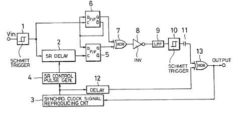
. 3 i~ nll cl~c~rio~l c~r~ult ot ollo e~RIn~ of "
dero-d~la~lon ~lrault ~Yhich l~ny b~ us~l to n~rry Ollt tlle Illv~rl-
ti~ t~ ir~lit, ~ lE)~ Ir~ lit~l t~
S~hlnitt trig~cr clro~lit ~, th~ out~lt ot w~ ppll~l(l tr.- nl~
S}~ (3hi~t r~ t~r) delny oSrolli t ~ hncl to a l)-ty~e fl i~)-f lop
. ~n S~ ~shift rcgister) aontrol pulse gen~rEItlrlg clr~ui~ ~1 is
~ontrolle~ ~y n synchron~zSng ~lo~k si~n~l suplied by n syncllro-
ni~ing clock sign~l reproduçln~ ~ireuit S whSoh re~elycs a clcn)o(l^
ulsted ~Z si~n~l from the ~utput o~ ~n E~L~ E OR (XO~ nte~
B. The SR dçlay clrcuit 2~ to which the output s~gnal of th~
Schmitt trSg~er circult 1 15 applled, receSvas the output pulse
signal of the S~ oontrol pulse geller~t5ng c~r~uit ~, to set a
delay tSm~.
The .output slgnAl of the ~R delay circuit ~, ~nd the
output si~nal ~f the Schmit-t -trigger circui~ 1 are a2plied to tl~e
clock input terminals C of D-type fli.p-flops 5 ~nd 6, respectively
and the Q output signal of the flip-flop 6 is a~pliecl to -~lle 1~ in-
~utterminals o the flip-flops 5 ~Id6. The Q o~i-tput sigl~als o.E the
flip-flops 5 and 6 ure appli~d to an P.XLU~IV~ OR (XOR) gatc 7 for
ph as~ compr~rison.
Th~ output signal of the ~OR ~ate 7 ;s supplied through
~n inverter 8, ~ low-p~ss fllter ~ .and a Sc~itt trig~er cir~uit
: 10 to n- capacitur so tllnt n ~C component is r~mov~d th~r~ror~i .
that is, the signrll AS sho~ ~n ~ig. ~(~) Is obtained, The sig-
nnl thlls obtained, ~nd a siennl obtAined ~y delaying by ~ prcde-
termlned pPriod o~ time the synchronl2ing ol~ek signal supplied
by the synchronizlng clock signal reproducillg clrcuit 3 !n dcl~y
circuit 12 ar~ Rpplie~ to XOR éute 13, 90 thnt the N~Z si~nal ~5
shown in Fi~. 2~H) is obtrlin~d.
- 12 -
: ' '
69~1~
.~ L~pnrcl\t fr~)ln ~ho nbt~v~ ~ln~scription~ tl~f ~. if~
~elt~o~ tlol~ al~c~t 1~ L~lvnllt~ o~l~l in ~}II~t It i~ t~
ly y ~lclclill~ th~ pncitor 11, tll~ ~01^~ n 13 Illld ~l)e ~.leln~
clrcuit 12 to n convel~tlon~ lny dcteatlon olro~lit; ~hht i~:~ it
the clrcuitry is ~Imple, and it cnn nccur~t~ly dcmo~ t~ tllc
signal ~ithout bein~ affected by vnrlatlonx of t~le c~rrier rrc-
quency,
The delay time ig set to T/~ In th~ derno~u1ntlon clr-
cult~ as ~Yas descrlbed nboYe- Thereforo~ the vQriation of thc
opersting ref~rence point o~ the phage co~p~r~tor ean be reduced
to ~ T4 ~ here ~ Is the variation Or ~ cArrlcr freq~ency),
with the result thRt stabllity ls much ImproYed.
Furthermore~ as the reference pha~e p~rt is providcd
bcfore RndJor ~ter the ph~se change part, interr~rcncc betw~cn
the signals in the time slots ~an b~ prcycnted dllrin~ demodula-
t I on . ~
In the a~ove-described embodlment, the p~asc is cil~nged
to~ ; howeYer, eYen If the clrcult ls so rnodlricd t}lRt the
phase Is ch~n~ed to an optlonal phase ~ , th~ circu~t c~n ope-
r~te in th~ 6ame manner.
~ igs. 4(~),,,4(E) are sl~tnal diaerAm~ uscful in ex-
plalnln~ Rnothar embodiment. The ernbodlment is ~iffercllt fro~
thP ~boy~-d~sçrlbed embodinlent only in that, ~s sho-Yn in Fig.
4(~), the ~irst hal~ of ~ phase changte p~rt correspon~lrlg to a
"mark" period ch~nges llne~rly to ~ and the second h~l~ chan~s
in th~ opposltc dlrectionJ while the first hall of ~ phase change
part corresponding to a l'spaee" pgriod ch~n~es line~rly to - ~
and t~e second half chan~e~ in t~le oppoSite direetion~ arld tllnt a
reference phasc part l~tg ~or a ~ivPn period of tilne ~ T.
,~ I - 13 -
:
12~;971~ 1
~r~r~ror~ if tll~ 9~ ow~ Jr~-
s~ntecl by ~ ~t~ thell tho dclnyecl ~igll~l o (t ~ n:
shc~Yn in ~ l tR) ~`hC dl ff~ren~e ~i~Jl~l O (t) - ~ (t ~ A 1~)
bet~Yeell th~ t~Yo gigTInls has R ~Yaveforrrl lYhlch~ tLS ~howrl In ~'ie.
~C), h~s ~xtrcmol~ steep rising and fall~ng ~o~nponents,
~ he dlfferenoe slgn~ lOWn in ~ig. ~(C) i~ ~upplicd to
a phRse co~parator h~vin~ a ch~r~cterlstlc aS sho~Yn in Fi~. 4(D),
so that ~n output ~Ynveiorm as sho~vn In Pi~. 4(E) is obtainetl.
~hat is, ~f, in the demodlllatlon circuit of Flg~ 3, the delny
ti~e ~y the SR d~l~y clrcu~t a Is s~t to ~ T, then th~ M~% si~-
n~l ~orrespondln~ to the ori~lnhl dlgltRl data Can be o~tained.
In the ~boYe-descrlbed embodiment, Incre~slng the time
T result~ in an increasb in ~nplit~de of the output si~n~l ol
the phase compar~tor, so th~t the "mark" ~nd "sp~ce" determina-
tlon ean be ~chieved with hlgher accur~y, wherea~ decr~aein~ the
tlme A T decreases the shlft- ~ n ~ ~ 0~ the phase reference
polnt due to the ~arrler frequency variation, so th~t stabili~y
i~ i~prov~d. ~ccordingly, tlmc ~ T 1~ set to ~ v~l~e ~Yhich,
dependi~ on the sy5tem emplo~cd, be~t mcets th~se contrA~ietorY
chRracteristlcs.
ln the above-~s~ribed e~bodi~nt, tlle phas~ ~h~n~es
lincArly; howeYcr, th~ circuit m~y be so modified that the phas~
chan~es a~ordirlg .~o ~ diff~ren~ n~notoT~e function Instcad of a
line~r fun~ti~n, b~t oper~tion is the s~ the above-deseri~ed
embodiment.
Figs. S(A)...5(E) are si~nal diagrams for a descrlption
of ~noth~r ~lobod3m~nt. This eT~bodlment i9 dif~r~nt fr~n ~he
above-dascribcd embodilnents in tllat~ ~s sho~yn in I~ig. ~), in a
_ 14 _
97~
p~ ;e c:hnn~e p~ t corr~pontlllls to n "~ark~' porlo~ e ~ nsc
cllnn~c~ to ~ ) 1t tho rl tArt ~n~ to O ~t t~f` r'll(~ le1'~'-
n~ n p~nse ~h~llsc p~rt aur~es~rldl~l~ to ~l "rl~.la~ (J,
pha~e chi~ngc3 t~ - a ~t thc ~tnrt and O a~ th~ ~nd~ ~nd in tl~t
phase rcf~r~ e pRrt lagt.g ior a pcriod of tlmo T/2.
~ ccordlrl~ly~ If th~ si~n~l of ~i~. 5(~ re~-res~nted
by a ~t~ then a delayed sign~l ~ (t - Tl~,) is ns sho~-n in Fi~.
5(B~. The dlfference sl~nal bet-Y~on the two signals is ~s indi-
cated in ~ig. 3~); that ~s, ehe ~YaYe~orm of the difference s~-
nRI Is xuch that the phase ~han~e9 to ~ in the flr~t half or a
t'markt' pcrlod and to -~ in the second half, ~nd it ch~rlge6 to
- ~ In tlle ~irst hRl~ of ~ "spao~ perlod and to ~ in the secon~
hal~
The difference si~nal of ~ig. 5((~ appl Icd to a
ph~se eompar~tor haYlng a ~har~erlr,t~c R5 sho~Yn in ~i~. S(D).
as ~ resu1t o whibh an output ~aveform as shown In Fl~. 5(~) is
obtalned. Thus, If in the demo~ulatlon.clrcuit of Fig. 3, the
delay tlme o~ the SR delay circuit 2 is set to.T/~, then an ~P~Z
sl~al correspond~n~. to the orlgSn~l dl~it~l d~t~ can be ob-
talned .
Flg. 6 Is an elect~ical circu~t ~howing Rnother e~llmplc
o~ the d~mo~ul~tlon cire~it~ The demodu1~tlon clr~ult of ~
.- Is dl~ferent fr~m tilat. of Fig. 3 only ~in that the inYert~l 8 is
ellminated, nnd the delay time of the delay ~ircuit 1~ is c~langetl
by ~ hai~ pcriod o~ the synchronizin~ ~loc~ sign~l froln th~t o~
he demodulation clrcuit o~ , 3.
i ~ 15~
~ ecordin~ly, in t}l~ cle~llotlllln~loll ~lrcul t of ~ , t)le
t~ igllnl o~ the ~h~l~e (~vrn~ rator is o~ c)~l l ta 11l Icvcl to
th~t of thc ~lln~ oom~tl~ntor ill thc ~lel)7~clulAtlc~n clle~ ot 1 i~.
3 ~a~3 Yig. 1(~)), nncl th~ ~ynchroni7~irl~ ck ~ ,rnAl ~ p~lie~l hy
th~ delay circult 1~ v ~)pposit~ levcl to th~lt ~ )plie(l
~y the del~y circ~lit 1~ In the demo~lulntlo~ ircu~t of ~Ig, 3
~ 7(B)). Thercfore~ when the two slgnal~ are ~ppl lcd to the
X~R gate l3~ th~ dernodulation circuit provldos the s~me N~U. slg '
nal (~1~. 7(C~ as the d~modulatlon ciruclt of Pl~. 3. '~ ;
~s d~scr~bcd abo~c, the modem sy~t~m of the invention
proYideS n transmission si~al whlch i~ PS~-modul~ted in ~uch
manner that a phAse- re~erenco part of ~ predetermlned tinle is
provlded` in the front and/or rear pn~t o~ ~ ti~e,slot of a dlgl-
tal pul~e si~nal, and th~ ph~se i~ ~hanged frcm a reference value
to a ~ir~t or sceon~ predetermlned value for a "mark" or ~spa~e"
respectiv~ly accorc3ln~ to a monotone ~unctlon in the ~irst hnlf
of th~ remaining period of time o~ the time ~lot and chan~ed in
the opposite dir~tion to the reference YAlu~ in the s~cond hnlf
of the remaining period~ rhere~ore~ thc m~dem system of the
InYentlon can obtain the ori~inrll dlg~tal s1~n~l re~dily and
accuratcly by mcan~ of a del~y deteotion systern1 1n wi~ \ the
signal is d~laycd ,as long a~ the time ~f the phsse reference
pRrt~ ~YItho~t bein~ ~f~eoted by any var~tions,in t~e -carrl~i .
frequency.
. Thus far~ desript~on 1las been made of the n~dulfltion
si~n~ls and the de-modulatlon cir~ult Ior demodul~ting thosc
slgn~ls. 'rhe rTx)dulation oircu~t~ th~selves~ tlre sirTlplc and
_16_
' ~
~
~ 6~7~ I
strni~h~.~ur~,srcl. ~ ita~l~ m~cIIllntioll oy~t~ for f,cncrn~ r~ ~"
~nodulnted si~n~1s shown In ~Ig~ 51~ in thc nE)E)Ilontio~ slI(.)rr
, 13 n n ~I l ~l .
. ~ 12 illustrate3 ~ n~o~lu1~tio~ elr(~Ilit in ~ IIe~
~lot~l~in~ sl~Ilhl ~olIrcc 101 hntI a data si~nIll soureo 103 nr~ pro-
YidetI. Thectc so-lrces rcsp~ctlYely procluoe ~intirI~ pulses Vc n~
data pul~es Yg. l`h~ tlmlng pu1~e Vc is supplie~l n~ ~n OUtp-lt
s~Yitehing slgnnl ~ nd is nlso RpplI~d to invertcr 105 to pro-
duce a ~i~n~l Y~i WI-ich is applied as one ~nput to an ~NV gatF
107. The other input to ~ND gate is the dnt~ signnl Ys~ Th~
output o~ the A~D gat~ 107 i~t ~ gecond swit~hing si~nal V~t2. The
r~1ntlonship of ~he ~w;t~hing signals prbduee~ by tho modulatlon
ciruuit sh~wn in ~lg. 12 is illustra~ed In Fig~ 13. ~s fiho~Yn
therein~ the ~ata sign~l produce~ a "t~ark't ~ ~marktt _ Ilspaeetl -
signal p~ttern. The ço~e~ponding swltc~ling ~ignAls Y~1 ~n~ YD~
generated by the rno~ulation circuit of ~Ig~ 12 Is also illus-
tr~ted. ~hc switchin~ ~ignal~ ~re Applied to a hybrld cir~uit
lO9 i11ustrRted in ~i~. 14. A ~arrler Is app1i~3 to the input
terrnlnal 111 and ths output a~ the hybrid circUit it tu~cn at
termin~1 113. The phu~& of the slgnal ~pplie~ ta the input term-
~na1 Yin Is ~hQnged in ~ccord~nce wlth the s~itehln~ si~n~ls YDl
and YD2 wllich ~re applie~ to a diode network 115. As sho~ In
Fig. 13, when botll swlt~hing 3i~n~1s YDi all~ ~2 are in ~ .low
~t~te~ the diode networ~ 115 cnu~es th~ hybr~d circuit 109 to
produce a ne~atiYe phas~ shift ~or the signal ap~lled at tho
termin~1 Vin to the hybrld oircuit 109. ~Yhen YD1 Is hlgh and V~
Is lo-~, a ref~rence phase pnrt i3 e~tablished rnennlng that no
- 1.7 -
~;26~7~
phase~ shi~t occ~lr~ in hybricl c.irc~lit :l.()9. Whel) V~
higll allcl VD~ is .low, a ~)o~c,ilive p,lclse slliCt is lel)(!ral.e(l.
~S SIIOWIl ill tlle Sigllal (li,l(Jr.llll ~ ~t) oE l~ re :l.8 1~
resu].tallt ou~l-llt from th~ hybr;d circu:it .i3 ~ ;0 s~ t
in a positive cl.ileet;on for a "marlc" sign.l:l. and a pllasc
shi~t .in a necJaklve cl.irectioll Eor a "sE)ace" s iCJIl-.l]..
With referenee to the signal patterll generati 011
systems suitable for ~he signal pattern shown in FicJure;
2~A) and 4(~) r a variety oE signals could be employcd
having various signal patterns produced by known
orthogonal phase modulation eireuits as di.sclosed, for
example, in IEEE Transactions on Vehicular Technology,
Vol. VT-30, No. 3, August 198,1, "~ Compact Spectrum
Constant Envelope Digital Phase Modulation"; IE~
Transaetions on eommunieations, Vol. COM-31, No. 5,
May 1983, "A New Cross-Correlated Phase-Shift Keying
Modulation Technique" or IEEE Transactions on Vehicular
Teehnology, Vol. VT-33, No. 3, Augustr 1983, ''Digi~c
Portable Transceiver Using GMSK Modem and ADM Codec".
Furthermore, it will be apparent to those
skilled in the art that the present circu.it may be
modified in accordanee with the funetion signal generating
eireuits diselosed, for e~ample, in IEEE ~`ransactions on
Communieations Teehnology, Vol. COM-16, No. 1,
February 1968, "Generation of Digital Si.gnaling Waveforms"
or IEEE 'l'ransaetions on Communieations, Vol. COM-25, No.
10, Oetober 1977, "A digital Filter-Modulation Combination
for Data Transmission".
- 18 -