Note: Descriptions are shown in the official language in which they were submitted.
PHASE -LOC KED LOOP C~ I RC 11 I T
This invention relates to a phase locked loop
circuit.
Background of the Invention
In order to transmit information over a signal
transmission channel, it is conventional to use the
information to modulate a carrier and impress the
modulated carrier on the transmission channel. At
the receiver, the received signal is demodulated
and the modulation function-is recreated, and the
transmitted information is extracted from the modu-
lation function. If the information to be trans-
mitted is in analog form, the modulation is
generally of the amplitude or frequency of the
carrier and the modulation function is able to vary
continuously, whereas if the information is in
digital form the modulation is usually of the phase
of the carrier, or both the amplitude and phase of
the carrier, and the modulation function is a pat-
tern having a finite number, generally an integral
power of two, of distinct states.
In the case of digital information, the epoch
over which information is transmitted is divided
into a succession of symbol intervals that are of
equal duration. During each symbol interval, the
modulation function assumes a state associated with
a given symbol and the phase (or amplitude and
phase) of the carrier at the transmitter remains
constant. In a ~iven symbol interval, a modulation
pattern havin~ 2k distinc-t states can be used ta
transmit k bits of information. Thus, a pattern
having two distinct states (i.e., binary modula-
tion) can be used to transmit one bit of informa-
tion during onc symbol interval, a modulation pat-
"
~{~
tern having four distinct states can be used to
transmit two bits, and so on up to a limit deter-
mined by the signal to noise ratio of the trans~is-
sion channel.
A common method of modulating a carrier in
accordance with a modulation pattern having four
states li.e., k = 2) is quadrature phase shift
keying (QPSK), in which the phase of the carrier is
modulated such that during any given symbol inter
val the carrier at the transmitter has one of four
discrete phase angles relative to a reference
carrier.
There are two types of QPSK modulation, namely
absolute QPSK and differential QPSK. In absolute
QPSK, the transmitted information is represented by
the phase of the carrier within a symbol interval
relative to the reference carrier, whereas in
differential QPSK the transmitted information is
represented by the phase of the carrier within a
symbol interval relative to the phase of the
carrier within the previous symbol interval, i.e.,
the phase shift from interval to interval.
QPSK modulation in a random data pattern sub-
stantially eliminates energy at the carrier frequ-
ency. Unless a reference carrier is added to the
signal or carried on a separate channel, a simple
PLL will not be able to regenerate the reference
carrier. However differential QPSK can be succes-
sfully demodulated if a local carrier of exact
frequency and stable phase is available. To detect
only changes in phase, the origlnal reference phase
is not needed~
A signal at the carrier frequency may be syn-
thesized by locking a signal at N times the carrier
fre~uency (where N is the number of phase states in
,",
. . .:..~. .
:
. . .
... ..
. :, . .
.. . .
n~
the modulation pattern, i.e., four in the case of
QPSK) to the received signal, and then dividing the
frequency o the signal by N in order to recover
the exact carrier frequency. This method is sub-
ject to the disadvantage that there is no necessary
phase relationship between the received signal and
the synthesized signal, and therefore an additional
step must be carried out in order to set the syn-
thesized signal to the desirecl phase. In addition,
this known method is difficult to implement at high
carrier frequencies.
U. S. Patent No. 4,308,505 discloses a circuit
employing a phase-locked loop ~PLL) in order to
synthesize a replica of the reference carrier.
Operation of the carrier xecovery PLL is dependent
on recovery of a timing signal related to data
transitions. The carrier phase is controlled
within the boundaries of a phase window by digital
feedback to a voltage controlled oscillator (VCO),
with the rate of change limited by a loop filter
The size of the phase window potentially increases
the data error rate of a data recovery system using
the PLL.
Summary of the Invention
A preferred embodiment of the present inven-
tion is a circuit that receives an input signal
that has a predetermined frequency during a succes-
sion of symbol intervals and of which the phase
during a given symbol interval is related to the
phase duriny a reference interval by the angle 2n~/N,
where N is a positive integer and n is an integer
in the range from 0 to (N-l), and generates a
refererl~e slgnal of which the phase has a desire~
rel3tic)rl~hjp to t}~e phase of the input signal
~2~7,'~
during the reference interval. The circuit com-
prises a controllable oscillator that is responsive
to a control signal to generate the reference sig-
nal, the frequency of the reference signal being
equal to the predetermined frequency when the value
of the control signal is zero. The circuit also
comprises a demodulator for generating a Eirst
signal representative of the sine of the phase of
the input signal relative to the reference signal
and for generating a second signal representative
of the cosine of the phase of the input signal
relative to the reference signal, and a function
generator for receiving the first and second sig-
nals and generating the control signal such that
when the phase of the input signal relative to the
reference signal is equal to 2n~/N plus the phase
of the input signal relative to the reference sig-
nal during the reference interval, the value of the
control signal is zero and the first derivative of
the value of the control signal with respect to
phase of the input signal relative to the reference
signal is positive.
Brief Description of the Drawings
For a bett~r understanding of the invention,
and to show how the same may be carried into
effect, reference will now be made, by way of
example, to the accompanying drawings in which:
FIG. l is a block diagram of a phase-locked
loop circuit embodying the present invention,
FIG. 2 is a vector diagram indicating the
carrier phases of a QPSK signal, and
FIG. 3 illustrates the waveform of a QPSK
signal over a succession of symbol intervals.
~6~
Detailed Description
The circuit illustrated in FIG. 1 has an input
terminal 2 at which it receives a signal comprising
a carrier wave that has been modulated in phase in
accordance with a modulation pattern having four
distinct states~ The carrier phases associated
with the four moduiation states are in quadrature,
and may be represented by the vectors
P1 . . . P4 shown in FIG. 2.
The received carrier might have the waveform
indicated at A in FIG. 3. As shown in FIG. 3, the
waveform epoch over which the signal is received is
divided into a succession of symbol intervals,
which are arbitrarily numbered 101, 102, 103 etc.,
in FIG. 3, and during each symbol interval the
received carrier has a constant frequency Fs and
has a constant phase. The phase Pi of the signal
during a yiven symbol interval is related to the
phase during the preceding interval by the equation
Pi=Pi_l+n~/2 (1)
where n is an integer in the range from 0 to 3.
Thus, if the phase P1 during the interval 101 is
taken as zero, the phase P2 during the interval 102
is ~/2 and the phases P4 and P3 during the
intervals 103 and 104 are, respectively, 3~/2 and
~.
The useful information conveyed by the signal is
contained in the phase difference Pi ~ Pi_1, and
therefore in order to extract the useful information
from the signal it is necessary to determine the value
of n. For example, the value of n for the change in
phase between symbol intervals 101 and 102 is 1, and
the values of n for the subsequent phase changes are 2
: . .
`
` . , ' .: '' '''':'
. . ~ ,.
~103, 102), 3 (104, 1031, 0 (105, 104) and l (106, 105).
Between consecutive symbol intervals is a data
transition, at which the phase of the carrier may
change. The data transitions are shown in FIG. 3
as being instantaneous, but it will be appre~iated
that there would in fact be a non-zero rise time
associated with any change in carrier phase.
Moreover, FIG. 3 illustrates the symbol interval as
being an odd number of half periods of the carrier
and shows the data transitions as taking place at
zero crossings and peaks of the carrier, but the
circuit shown in FIG. 1 does not require any
specific relationship between the symbol interval
and the carriex period, and therefore the transi-
tions need not take place at any particular pointin the carrier cycle.
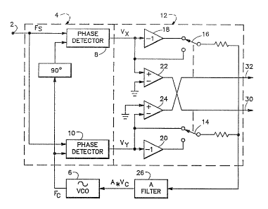
The input siynal received at the terminal 2 of
the circuit shown in FIG. 1 is applied to a
demodulator 4 that also receives the output signal
of a voltage controlled oscillator (VCO) 6. The
demodulator comprises a pair of phase detectors 8
and 10 that are driven in quadrature by the output
signal of the VCO 6.
If the phase angle of the output signal of the
VCO relative to the input signal at the terminal 2
is P, then the output signal of the phase detector
8 is a voltage Vx that is proportional to cos P and
the output signal of the phase detector lO is a
voltage Vy that is proportional to sin P. The
locus of the points (Vx, Vy~ in the vector diagrarn
of FlG. 2 is a circle 28 having its center at the
point of intersection of the phase vectors Pl . . .
P4 and of radius equal to the length of the
vector 9 .
. . .
: ' .
r 1~f~
The output signals of the phase detectors 8
and 10 are applied to a function generator 12. The
function generator comprises switches 14 and 16,
inverters 18 and 20 and high gain comparators 22
and 24, and provides an output signal of voltage Vc
which is given by the following equation:
Vc = S1 ~ Vy + S2 vx (2)
The values of Sl and S2 depend on the states
of the switches 14 and 16 respectively, and the
states of these switches in turn depend upon the
signs of Vx and Vy respectively. Thus, if Vx is
positive, the switch 14 selects the input of the
inverter 20 and S1 is equal to +1. If Vx is
negative, the switch 14 selects the output to the
i.nverter 20 and S1 is equal to -1. Similarly, if
Vy is positive, the switch 16 selects the output of
the inverter 18 and S2 is -1, whereas if Vy is
negative the switch 16 selects the input of the
inverter 16 and S2 is +1.
The output signal of the function generator 12
is applied to a loop filter 26 having a transfer
function A and the loop filter applies an output
voltage A*VC to the control input of the VCO 6.
The output signal of the VCO 6 has a frequency Fc
which is given by
Fc a Fo + A * Vc
where Fo is the nominal frequency of the oscillator.
In order for Fc to be equal to Fo~ Vc must
be equal to ~ero and therefore S1*Vy must be equal to
-S2*Vx. This relationshlp i.~ sat.isfied for four
. :: . . . :.. . .
: , :
... . ......
values of P, indicat~d in the followlng table.
P VX VY Sl S2 VcdVX/dP dVy/dP dVC/dP
.
~/4 +.707 +.707 +1 -1 0 -.707 *.707 +1.414
3~/4 -.707 +.707 -1 -1 0 -.707 -.707 ~1.414
5~/4 -.707 -.707 -1 +1 0 ~.707-.707 +1.414
107~/4 ~.707 -.707 +1 +1 0 ~.707 +.707 +1.414
It will be seen from the table that the phase
angles for which Sl~Vy is equal to -S2*Vx are in
quadrature.
It will also be seen that for each value of P
for which Vc is equal to 0, the first derivative of
Vc with respect to P is positive and therefore the
first derivative of Fc with respect to P also i5
positive, i.e. is such as to force the frequency Fc
to change so as to maintain a constant phase
relationship between the carrier and the output
siqnal of the VCO 6. Accordingly, the two
conditions for a stable phase lock apply when P has
any one of the above four values. Consequently,
when a QPSK signal having a carrier frequency Fs is
applied to the terminal 2, the phase-locked loop
will lock to one of the modulation states of the
input signal. The frequency Fc of the VCO's output
signal will be equal to Fs and the VCO's output
signal will be shifted in phase from the input
signal by (2n~ /4. Once khe output signal o~ the
VCO 6 has become locked to the input signal
received at the terminal 2, regardless of the
modulation state of the input signal at the time
that loclc is achieved, the output signal remains
,~ . .
- : . .~ '
1` ..' ~ .. '
' '
'
~ .
,,~, .
. ...
g ~L2~
locked to the input signal a~d will not change in
phase relative to the reference carrier or in
frequency so long as the modulation pattern of the
input signal conforms to the four states. The data
can then be recovered by logical interpretation of
the output signals provided by the comparators 22
and 24 at the terminals 30 and 32 respectively.
The transfer function A of the loop filter 26
is such that the expression A*VC has a term propor-
tional to Vc and a term proportional to the integral
of Vc with respect to time. Consequently, the
phase-locked loop is a second order loop and is able
to achieve a zero phase error between the signal at
the terminal 2 and the output of the VCO 6. It is
necessary ko have a zero phase error, or at least a
known phase relationship, between the signals in
order to be able to recover the data used to modu-
late the carrier. However, even if the transfer
function A were such that the expression A~VC did
not include a term proportional to the integral of
Vc, i.e., the phase-locked loop was a first order
loop, the data can be recovered if separate means
are used to determine the phase relationship between
the output signal of VCO and the carrier phases.
In order to ensure that data transitions do
not disturb the phase-locked loop, the rise time of
the data transitions must be less than the response
time of the loop filter and greater than the rise
time of the carrier channel.
An embodiment of the invention was constructed
with the following parameters:
Carrier frequency (Fo) 6 MHz
Symbol interval 1.29 s
Bandwidth 1 MHz
Modulation Differential QPSK
:. :~ .;
: ~ . . . ,
.:
- ::: :
' :: ~" :;. ' ':
: ::: : ,, :: :
: : : :, .: . . :
~IL2~ s~
1~
In operation of this embodiment, the output
signal of the vCO remained locked to the input
signal with a carrier to noise ratio of less than
12 dB. The bit error rate was less than one part
in 100,000 at a carrier-to-noise ratio o~ 15 dB.
It will be appreciated that the invention is
not restricted to the embodiment described with
reference to the drawings, and that modifications
may be made therein without departing from the
scope of the invention as defined in the appended
claims and equivalents thereof. For example, the
voltages Vx and Vy need not be proportional to
sinusoidal functions of the phase difference P, so
long as they define P unambiguously. It is in fact
preferred that Vx and Vy be linear functions of P,
such that the locus of points (Vx, Vy) in the
vector diagram of FIG. 2 is not a circle but is a
square 34, as shown in dashed lines. In the case
of the locus being a square having its sides per-
20 pendicular to the vectors P1 P4, the values of
Vx and Vy are substantially equivalent to the
cosine and sine respectively of the phase diffe-
rence between the input signal and the reference
signal. The invention is not restricted to use
with differential QPSK modulation, and may be
applied to absolute QPSK modulation provided that
it is possible to determine which of the carrier
phases i5 the reference phase.
.
.
,