Note: Descriptions are shown in the official language in which they were submitted.
6~ 7
~Q~
The lnventlon d~sclosed herein rel~tes
generally to ~all effect and 6~milar sensor~
characterized by ~ensitivities which vary
significantly with temperature, and more par~icularly
to integra~ed circuit ~all e~fect devices with means
for achieving æubstantially temperature independent
sensitivity.
lo ~all effec~ sensors are recognized as
offering substantial advantages in many sen6ing
applications. For some time, such sensors have been
widely u~ed where an on-off or binary ou~put i8
required or acceptable. ~all effect 6ensors have also
been u ed in various applications r~guiring analog
outputs. ~owever, such u~e~ have been limited because
the output voltage of a ~all element i~ 80 low tha~
amplification i8 requlred, and, ~ince the Hall element
sensitivity varie~ with temperature, the amplification
~u~t al~o be made to vary w~th temperature in a
compensating mann~r~
It has been common to utilize expensiv2 and
bulky precisîon ampli~iers and compen~ation circuitry
in at emp~ to achieve acceptable accuracy, including
~ .
.
.
~; ~ --- ; : ,
....
~' ~' ' ` - '
~6~37~
-2- 6~159_995
lin~arity and ~tability over a temperature ~nge.
However, even the~e meaAure~ have not r~uulted ln
sufficient accur~cy ~or many appl1~ation~. ~urther,
many applicatlon~ for which the accuracy requ~rements
could be met with known amplification and compenæatlon
~ circuitry cannot support the high c08t of such
I circuitry-
The applicant ha~ devi~ed 2 unique integrated
circuit ~all effect device in which the ~all effect
element and portions of amplifier gain control and
responsivity tracking resistors are formed in ~he ~ame
epitaxial layer, thereby providing precise temperature
compen~ation with very compact and inexpensive
circuitry which further features v~rious convenient
offset and null adjustments to facilitate set ing the
device for preci~ion tempera'cure independent
operatlon.
The invention ~ s an integrated circuit ~all
e$fect or simila~ ~ensing device with means f~r
providing temperature independent ~en~i~ivity. The
devlce compri~es a ~all effect element formed in an
epitaxial layer and amplifier means i~cluding re~istor
means of which a portion is formed in the ~a~e
epita~ial layerO The amplifier means may comprise a
fir~t amplifier ~tage formed of a pair of ideally
identical amplifiers connected in a voltage to current
: ' '`' '~
: , ~ .: ,
conver6ion (transconductance) arrang~ment, a second
a~plifier stage configur~ fo~ curr~nt to voltage
conver~ion (t~an~resistance) ~nd ~ current mlrror
lnterface conneating th~ ~irst and second amplif~er
stage~. ~he fir~t amplifier stage may includ~ a bi~s
. resistor of whlch a portion i5 formed in the epi~ax$al
layer. ~he second a~plifier stage lnclud~ adju~tment
means having a resistor of which a portion ~ 8 also
formed in the epitaxial layer fo~ adju~ting the rate
of change of transre~i~tance with ~espect to
lo temperature.
The ~ir6t and second amplifiers in the ~irst
amplifier stage may be cross coupled through an input
offset adju~tment ci~cuit to minimi~e unbalancing of
the amplifie~s. The amplifiers each have fir~t and
second input terminals of which the f ir~t input
terminals are connected to the ~all effect element and
the second input terminals are connected to separate
ends of a transconductance adju~tment re~ietor. An
output bias re~erence current through the amplifiers
~8 controlled by the bias resistor. A multiple of the
current through the transconduc~ance adjustment
resistor is transmitted through the current mirror
interface to the resistor in the adju~tment mean~ in
the second ampligier stage.
. .
7~
~ 6~15~-995
The firs~ amplifier stage may also be provided with an
output offset adjustment to permit further rnin.tmization of any
offset errors introduced by the ampl:Lfler stacJe. The second
amplifier stage may be provided with a null ad~ustment to permit
the device output voltage at zero applied magnetic field to be ~et
anywhere within the normal output volkage swing.
In accordance with the present invention there is
provided a temperature compensated integrated circuit Hall effect
device comprising: a substrate having an epitaxial layer thereon;
a Hall effect element formed in said epitaxial layer, said Hall
effect element having first and second output terminals between
which is produced a voltage difference indicative of the magnitude
of an applied magnetic field; and amplifier means connected to the
first and second output terminals of said Hall effect element for
receiving a voltage difference produced in response to a magnetic
field and producing an output voltage whose magnitude is
substantially linearly related to the magnitude of the magnetic
field over an extended temperature range, said amplifier means
including resistor means having a first resistive portion formed
in the epitaxial layer and a second resistive portion having a
~ constant temperature coefficient.
- In accordance with the present invention there is also
provided a temperature compensated integrated circuit Hall efect
device having a voltage supply terminal, a reference voltage
terminal and an output terminal, the Hall effect device
;~ comprising: a substrate having an epitaxial layer thereon; a Hall
.'' ~ ,.
.`~
7~3~
~ G~159--9~5
effect element formed in said epitax~al ].ayer, sald Hall effect
element bein~ ope.rable to produce a voltaye clif~erence betweerl
flrst and second -terminals thereof when an elee~ric current is
caused to flow between third and fourth ~erminals ~hereof and said
element is subjected to a magnetic field; a voltage supply
conductor connected to the voltage supply terminal; a reference
voltage conductor connected to the reference voltage terminal;
first and second ideally identical amplifiers, each having first
and second input terminalsr an input offset adjustment terminal, a
temperature traekiny bias terminal and output terminal means, the
first input terminals of the first and second amplifiers being
connected to the first and second terminals respectively of said
Hall effect elementr the input offset adjustment terminals of said
first and second amplifiers being connected to said voltage supply
~; conductor through first and second input offset adjustment
circuits respectivelyr the temperature tracking bias ~erminals of
:~ said first and second amplifiers being connected to said reference
voltage conductor through bias resis~or means including a first
resistive portion formed in the epitaxial layer on said substrate,
and the outpu~ terminal means of said firs~ and second amplifiers
BRIEF DESCRIPTION OF THE DRAWINGS
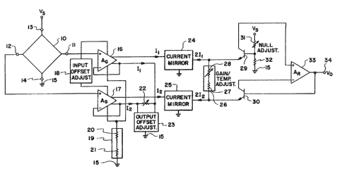
Figure 1 is a functional diagram partially in block form
- of a preferred embodiment of a Hall effect device in accordance
with the present invention; and Figure 2 is a schematic circuit
diagram of the Hall effect device of Figure 1.
:,, '
.", ..
' ,~' ''- ,~ ,,, ~.
9~
4b 6~159-995
DE R PTION OF THE PREE`ER~ED EME~OD~LME~NT
In the diagram of FlcJure 1~ reference numbera:L 10
iden~ifies a Hall effect element having output terminals 11 and 12
between which a voltage is produced when an eleckrlc current is
caused to flow between input terminals 13 and 14 and the element
is subjected to a magnetic fleld. Hall effect element 10 may be
formed of N-epitaxial material by conventional processes in an
epitaxial layer on a semiconductor substrate along with the
circuitry for providing output signal amplifaction and temperature
independent sensitivity compensation. The Hall effect
:~ :
-5-
~lement preferably contain~ two identical elements
plAced in an integrated circuit l~yout ~u~h that th~
supply c~rrent directions ~re orthogonal ~o ~8 to
reduce mechanlcal ~tre~B effect~l Xn soma situations
it may be ad~an~a~eou6 to u~e more than two elements,
A8 shown in Figure l, current ~ 8 cau~ed to
flow between inpu~ terminal~ 13 and 14 of ~all effect
element lO by connec~ing the terminals to a voltage
&ource Vs and ground 15 re~pectively. Ou~put
terminals ll and 12 are connected to fir~ and second
lo input terminal~ respectively o~ a fir~t amplifier
stage compri~ing a pair of ideallY identical
amplifier~ 16 and 17. ~mplifier~ 16 and 17 are cro6s
~- coupled through an input offse~ ad~ustment circuit as
indicat~d by block 18. They are al~o connected to
ground 15 through a b~aR circuit l9 which operates to
trac~ the responsivi~y of ~all ef~ec~ element lO. For
that purpose, bia circuit l9 include~ ~eries
connected re~i~tor~ 20 and 21, of which resi~tor 21 i~
~ormed in the same epitaxial layer as ~all effect
element 10.
The ~irst stage ampli~i*r i8 a
transconductance amplifier having unity voltage gain
and a transfer conductance equal to the difference in
the output currents o amplifier~ 16 and 17 divided by
the d~ ference in voltages between Hall effect device
output tarminals ll and 12. Tran~csnductance
- . - . . -
-,.'' '
,::
-:
~d~u~tment ~ the flrst ~t~ge amplif~er i~ peovided by
mean~ of a v~riable re~i~tor 22 shown connected
between tran~conductance adjustment node~ at opposlte
end~ of th~ re~l~tor. The first a~plifier stage i8
al~o proYided with an output of~set ad~ustment circuit
indicated by block 23 connected from the
tran~conductance adju~tment nodes to ground 15.
The first amplifier stage produces a pair of
current~ Il and I2, the difference of which represent
the magnitude of the magne~c field applied to ~all
~ffect element 10. Currents Il and I2 are supplied to
the tsansconductance adjus~men~ node~ and ~o current
mirror~ 24 and 25 which are con~tructed to produce
current doubling and cause cu~rents 2Il and 2I2 to
flow to a second amplifie ~tage.
The ~econd ampliier stage i8 a ~orton
amplifier having unity voltage gain and a ~ran~fer
re~istancs equal to the output voltage differenti~l
divided by th~ input current differential of the
stage. The ~econd amplifier 6tage include~ adju~tment
~ean~ identiied by reference numeral 26 for adjus~ing
the rate of change of transresis~ance of the ~econd
stage wi~h re~pect to temperatureO A~ illustrated,
adju~tmen~ mean~ 26 comprise~ two resistors 27 and 2B
connected in series. Re~istor 27 i formed in the
same epitaxial layer as ~all effect element lO.
~ 76~
_7 _
A~justment m~ans 26 iG connected b2twe~n the
emitter~ o~ a pair of NPN transi~torA 29 and 30 whlch
orm part o th~ second ampllfler 8ta~e4 The base of
tran6i8tor 29 is connected to null adju~tm~nt mean~ in
the form of a voltage divider comprising a Yar~ble
resi~tor 31 and a fixed re~stor 32 connected in
serie~ between voltage source V~ and ground 15. The
collectors of transi6tors 29 and 30 are ~onnected to
noninverting and inverting current input terminals
respectively of the differential amplifier 33. The
outpu~ signal of amplifier 33 form~ the output signal
V0 on output terminal 3~ of the ~all effect devicer
and iB al~o supplied back to the base of tran~ or
30.
In the circuit diagram of Figure ~, the ~all
effect element and it~ terminals, the reference
voltage source or g~ound, the two a~plifiers forming
the fi~st amplifier stage, the resi~toes comprising
the bia~ circuit9 the first stage transconductance
adjuatment re~iskor, the two current mirror~, the
re~istor~ in the adju~tment mean~ in the second stage,
the null adju~tment re~i~tor~, and the device o~tput
terminal are identified by the ~ame reference numerals
as in F~gure 1. In Figure ~, reference numeral 35
identifie~ a voltage ~upply conductor connected to a
source of supply voltage Ys identified by reference
~ 7
numeral 36 7 Re~erence numeral 37 identif ie8 ~
raference volt~ge conductor conn~cted to a ~ource of
refarenc~ volta9e or ground 15. ~all effect element
10 i8 connecte~ directly between the ~oltag~ 8upply
and r~erence voltage conductor~ 35 and 37 to achieve
ratiometric charaoterist~cs o sensitivity, i.e., the
~all effect element output voltage always varies by
the same percentage as the supply voltage.
Al~o connect~d between conductors 35 and 37
iB a ratiometric current source which, in preferred
form, comprise~ an NPN transistor 38 having it~
collector connected to supply conductor 35 through a
: re~istor 39. The base drive signal for transi~tor 38
is supplied through an NPN transi~tor 40 having i~
collector connected to supply conductor 35 through a
. 15 re~i6to 41 in ~eries with a PNP tran~i~tor 4~. The
baæe o~ transistor 40 is connected to the collector of
transi~tor 38, and it~ emitter i8 connected to the
baae o~ tran~i~tor 38 o a~ to provide baae current
loading compenæàtion.
The emitter of tran~istor 40 i~ al80
connected to reference voltage conductor 15 through an
NPN tran~istor 43 arranged as a diode, and a resi~tor
44. The diode formed by transistor 43 matcheA the
characteri~tic~ of transistor 38. The emit~er of
tran~iætor 38 ia connected to reference voltage
conduc~or 15 through a resistor 45 and an NPN
tran~i~tor 46 arranged as a diod~.
'`' ~ :,.. :, .
- - . . . ..
~ 7~
The ba~e dr~ve ~ignal ~upplled to tran~l~tor
~0 i~ also ~upplled to an NPN transistor S0 who~e
collecto~ i~ connected to ~upply conducto~ 3S through
a series connected re~istor Sl and a transl~tor 52
arranged as a dioae, and whose emitter iB connected to
the emi~ter of tran6istor 40. It can be shown tha~ i~
the resi~tance of resi~tor 39 iE t~ce the re~istance
of re~l~tor 45, the base-emitter voltages of the
tran~i~tors cancel out, and the voltage at the emitter
of transi tor 43 i8 temperature independent and
ratiometr~c with the supply voltage.
Amplifier 16 ha6 first and ~econd input
~erminalæ of which the fir~t input terminal i8
connec~ed to output terminal ll of ~all effect element
lO. Node 53 which i~ ~hared with amplifier 17, is
connected to the ratiometric cursent sourGe æo a~ to
provide Early effect compensation. The fir~t input
terminal of ampl1fier 17 i8 connected to output
termin~l 12 of ~all effect element 10.
Ampllfier~ 16 and 17 in combinatlon with
Yar$able control re~i~tor 22 form a voltage to current
converter. This scheme force~ the ~all effect element
loading current~ to be independent of both the gain
re~i~tor value and the input signal from the ~all
effect element, as i8 nece~sary to achieve temperaturP
independent sen6itivity,
-. , '- -
:;-'' : , :
. . .
.
--10--
P~e8i6tol: 22 i8 pref'erably an external thlck
f~lm laæer trimmable resiæ'cor. Ampliflers 16 and 17
form ~ balanced pair, and are cros~ coupled through an
input of~et ad~ustment circuit w$th cro~ coupling
compenE,ation, described in more detail hereinafter.
The ampli~iex~ are connected in a unity voltage gain
configuration, and the voltage across re~istor 22 i8
equal to the 9UtpUt voltage of the ~all effect
element. The signal produced by the f irst amplif ier
stage i8 the ~i~ference between the output currents
produced by amplif iers 16 and 17, and it proportional
to the voltage acros~i re~istor 22.
Th~ preferred construction of amplifiers 16
and 17, of which only amplif ier 16 will be
specifically described~ include, an NPN tran~i~tor 60
whose base electrode compri~e~, the Pirs~c input
ter~inal of 'che amplifier, and whose e~nitter electrode
i8 connected l:o one end of resistor 22. The collector
of transi~tor 60 and the base of ~n ~aPN tranæiE,tcr 61
are conn~cted to the input offE,et adju~tment circuit.
Amplifier 16 further include, a multiple
collector PtapJcrall~istor 62 having its emitter
connec~ced to supply conductor 35 and one collector 63
connected to it~ base. Collector 63 i~ al60 connected
to the collector of an NPN transistor 64 ~hose ba~e is5
connected to node 53.
`
.
.
A ~econd collector 65 o t~an~1~to~ 62 ie
connet~ted to ~h~ emitter of tr~n~i~to~ 50 and provide~
a feedback current. A thlrd collector 66 o
trans~stor 62 produces a current which comprise~ one
input signal to the ~econd ~mplif ier ~tage . Thi~
output current ia supplied through an NPN tran6istor
- 67 which is interconnected with a PNP tran~i~tor 68 'co
provide Early effect or base wid~h modula~ion
compensation with re~pect to temperature changes.
Currents through collector~ 65 and 66 of
transistor 62 are produced regardless o~ whe~her there
i~ a magnetic f ield applied ~o ~all e$fect element
lO. When there is no applied magnetic field, the
required current i temperature independent. When
there is an applied magnetic field, the portion of the
15
current due ~o the ~ield i8 temperature dependent.
Compen~ation tracking ~or the currellt bias of
~ifferen~ial tran~i~tor pair 61, 64 i~ provided by-
supplying the current bia~ through ~eries connected
bi~ re~i~tor~ 20 and 21, of which re~istor 21 i8
formed in the epitaxial layer . ~y appropr iately
proportioning the resistances of re~i6tors 2û and ~l i
the bia~ current may be made to track the respon~ivi~y
of ~all ef ~ec~ element lO .
,;
-
,
7~1
-12-
The source o~ th~ bia~ current i~ an N~N
trdn~istor C9. Speci~ically, the collector o~
tran~lsto~ 69 i~ connected to the ~mitteE~ o~
tran~istor~ 61 and C4 and the emitter o~ tran~l~tor 69
iB connected to ground 15 through r~sl~tors 20 and
21. The ba~ drive for transistor 69 i8 provided by a
reference circuit 70 which also provide~ ~he baQe
drive for ~orre~ponding tran~istor 69' in amplifier
17, and for current source transi~tors used ~n
conjunotion with output off~et trim re~istors aæ i~
lo noted hereina~ter.
Amplifier 17 i~ ideally ~dentical to
amplifier 1~. ~owever, ~mall difference~ in
performance parameters occur ~ecause of unavo$dable
fabrication proce~ variations. In addition, the
amplifiers may exhibit amall input off~et voltage~
which mus~ be compens~ted for becau~e the Hall elemen~
output cignal i~ small and high accuracy i~ required7
~ore p~rticularly, if the base-emitter voltages o~
translstor 60 and corre~ponding tran~ or 60' in
amplifier circuit 17 are not equal, a temperature
error term will refiult at the input to the fir~t
amplifier s~age. Since this error i~ at tbe input, it
is very ~ignificant due to the gain ~ultiplica~ion of
th~ circuit. Input off~et adjustment i8 accomplished
by trim resis~or 71. A second trim resi~tor 72 may be
provided to ~urther facilitate input offset
adjustment.
': ' :
.
: ''` . '` ,
'; ,
-13~
The in~ut offset adju~tment c~r¢uit 1~
comb~nad w~t~ a cro~ coupling arrangement including
du~l collector PNP transi~tors 73 and 74 that ~llows
the current densit~e~ of the base-emitte~ ~unctions of
transi~tor~ 60 and 60' to be adju~ted without
unbalancing the output. Cro~s coupling i~
accompliRhed by forcing the di~erence of the current~
into the node~ at the ends of resistor 22 to remain
constan~ regardle~ o~ the base-emitter current
densitie~. As the ba e-emitter current density in one
lo of tran~i~tor~ 60 and 60' i8 increased due to
trimming, the current into the as~ociated node of
resl~tor 22 increases. 80wever, the circui
concurrently add~ the same amoun of current ~o the
other node of resi~tor 22, resulting in a con~inuou~ly
balanced ~t~te.
Collector 75 of tran~i~tor 73 i~ connec~ed to
-: the base of an NPN tran i~tor 7C whose emitter i8
conneeted to the collector of a tr~nsi~tor 61' in
amplifier 17. Collector 75 i~ also connected to the
coll~ctor of transi~ o~ 60 through an NPN tran~istor
77 arranged as a diode~ Collector 78 of tran~istor 73
and a collector of multiple collector PNP transisto~
62' in ampl~fier 17 are connected to the node in
amplifier 17 at one end of resistor 22.
: 25
l',.~
. ~:
,.. .
, , .:
7~
-14- 6~159-995
. Slmilarly, collector 79 o tran~l~tor 74 1
connected to the base o~ an NPN transi~tor ~0 whose
emitter i~ connected to the collector o~ transistor 61
in amplifier 16. Coll~ctor 79 i8 al80 connected to
~he coll~ctor of tr~nsi~tor 60' through an NPN
tran6i~tor 81 a~ranged a6 a diode. Collector 82 o~
transistor 74 and collector 65 of multiple collector
PNP tran~istor 62 in amplifier 16 are connected to the
node ~n amplifier 16 at the other end o~ re~istor 22.
The ccllector8 of tranBistors 76 and 30 are conn~cted
to voltage supply conductor 35 through resistors ~3
and 84 refipectively.
The ba~e curren~ of transi~tor 61 i~
approximately equal to the base current of tran~i~tor
80, and the base current of tran~itor 61' i~
approximately equal to the ba~e current of transi~tor
76. Th0 collector loadlng o tran~istor 60 equals the
sum of the base currents o transisto~ 61 and
tran~lstor 76. Likewiset the collecto~ loading of
tran~to~ 60' i~ equal to the ~um of the ba~e
currents o~ transistor 61' and transi6tor 80. Thus,
the co~lector loading currents of tran i~tors 60 and
60' are constrained to be equal.
Reference numerals 85 and 86 identify
capacitors which, in combination with tran~i~tor~ 76
and 80 and re~i~tor~ 83 and 84, provide frequency
: " '-'"' .
-15-
compensat1on o~ stable op~ratlon. Diode~ 81 and 77
bla~ tran~istors 76 and 80 and ~180 l~w~ the voltage~
acro~s capacltor~ B5 and 86 to achieve highe~
capacitance per unit area, thereby faoilitating
c~rcuit integra~ionJ
Transistors 67 and 68 compensate ~OÆ ~arly
ePfects in transistor 62 by providing the sam~ bia~
voltage temperature characteri~tics for collector~ ~5
and 66. Likewise, tran~istor~ 67' and 68~ in
amplifier 17 perorm a similar function with respect
lo to ~ransi~Sor 62'.
Temperature compenæation of ~he overall gain
o~ the ~all effect device will be discussed i~ greater
detail hereinafter. Xt is, however, poin~ed out that
in order to achieve such compensation without a null
sbift, the vol~age acro6~ resistor~ 27 and 28 mu~t be
zero with no applied magnetic field. This adjustment
i8 made with output o~f~et trim reslstor~ 92 and 93.
Re~i~tor 92 in serie~ with a current source transistor
94 i5 connected between the node in a~plifier 16 at
2 one end of resistor 22 and ground 15. ~imilarly,
re~i~tor 93 in ~eries with a current source transistor
95 i8 co~nected between the node in amplifier 17 at
the other end of resistor 22 and ground 15. The base
drive signals for transistor~ 94 and 95 are provided
by reference circuit 70. Resistors 92 and 93 can ~e
.. -
,, ~: . .: ~ -
' ~ :
~16-
trimmed to adjust the voltag~ acros~ res1fitor~ 27 ~nd
~8 to 2e~0 for null condition tsmperature
compen3a~ion.
~he output slgnal currents o~ amplifier6 16
and 17 are suitably multiplied, pre~erably by ~ factor
of two, and supplied to the seoond ampli~ier ~tage by
mea~s of current mirror~ 24 and 25. In current mirror
24, NPN tranRi~tors 100 and 101 form a convent$onal
current mirror. NPN transi~tor 102 operates to
compensate for the e~fect~ of ba~e loading currents.
lo The emitter of tran~ or 102 i~ maintained ~t one
emitter-ba~e voltage drop above ground by transistors
103 and 104 arranged a series connected d~odes which
are supplied with a positive voltage bia~ through PNP
tran~i~tor lOS. Tran~istor 106 functions to
compen~a~e for Early e~fects. Current mirror 25 i~
identical to current mirror 24.
In the second amplifier ~tage~ the input .
current differsnce is forced to ~lo~ through re~tors
27 and 28~ thereby creating an output voltage
-
re~erenced o an externally ~dju~table voltage at a
null circuit divider node. The null circuit i8
identified in Figure 2 by reference numeral 108.
Circui~ 108 includes a voltage divider comprising
adjustable resi~tor 31 and resistor 32 connected in
series between voltage supply conductor 34 and ground
15. P~P transistor 103 in combination with resi~tor
.
~ `
-17-
110 form~ ~ current ource which biases ~PN tran8i~tor
. TrAn8~tor 111 i8 controlled by curr~nt ~ource
tran~l~tor 112 whose coll~cto~ 1~ conn~cted to the
base and collector o~ transi~tor 111, and whose
emitter i~ connected to ground 15 through a re~&tor
113. The loading ef~ec~ o~ the voltage dlvlder can,
thus, be made very ~mall, the eff2ct of whlch i~ to
minimize any temperature drift of the null voltage~
The voltage signal produced by transl~tor 111
is supplied to the ba~e of an NP~ transi~tor 116
lo throuqh ~P transi~ ors 117 and 118~ Transi~tor li7,
togethee with transistor~ 111 and 112 are nece~sary
primarily to match corresponding transistors which
provide outpu~ fault protection as i8 deæcribed
hereina~ter.
15 The emitter of tran~istor 116 and the ~mit~er
of a corresponding transi~tor 120 are connected ~o
opposite ends o~ the serie~ combin~io~ of resl~tor
27 and 28~ ~ran~stor 120 receives a f~ed~ack signal
from a pu~h-pull output circuit 122 through an
arrangement of transistors 123-126 corresponding ~o
transistor arrangement 111, 112, 117 and 1180
Tran~istor~ 123-125 are nece~ary primarlly to provide
output fault protection. The voltage feedback to tbe
base of transi~tor 120 forces the emitter curren~& of
transistors 116 and 120 to be equal. Thus, when ~he
output curren~s of current mirror~ 24 and 2~ are equal
~.
9~ 6'
-18-
tbe~e i~ no voltage drop across re~i~tor~ 27 and 2B,
an~ thQ output voltage VO ~n output t~m~n~l 3~ 1~
equal t~ the voltage at ~he null circui~ divider node.
~ he base~ o tran~istors llC and 120 are
connected to the collectors o~ ~ du~l collector PNP
tran~istor 128 who~e emi~ter is connected to voltage
supply conductor 35~ The collectors of trans~stors
116 and 120 are connected to voltage s~pply conductor
35 through a transconductance reduction c~rcuit 130.
The need for circuit 130 ariies because, if
1~ ~he input currents to resi tors 27 and 28 are too low,
... .
the se~i~tor~ would be required to haYe a large
resiRtance, and would con~ume too much chip area.
~owever, the current at the base o~ ~PN transistor i31
must be ~mall so that compensation capacitor 132 can
be made small for minimizing chip area, while
remaining adequats to produce a stable phaEe margin.
Thus, current reduction may be achiev~d by using
curren~ m~rrors comprising dual collector PNP
transi~tors 133 and 134 which preferably produc~ a
reduction of about 20 to 1. The active load i then
for~ed by a current mirror compri~ing NPN transistor6
135 and 136. Transistor 137 compensates for the
effects of base loading currents, and achieve~ the
same collector bias for transi~tor 133 as transistor
131 doe for transistor 134 in order to compensate for
Early effects in transis~ors 133 and 134~
,, ~ '
.... .. .
:
7~
-19-
NPN tran~i~torg 139 and 140 whose emit~er8
~re connected tn re~rence voltage conductor 37
th~ough a resistor 141 form current Rource~ connected
to the emitters of tran6i~tors 131 and 137, and help
e~uali2e the base~em~tter voltage~ of the t~ans~stors
for better Early effect compen~tion. The current
re~uction ~cheme al~o allows a larger vol~age swing at
the base of transi~tor 120 than if a PNP active load
were used. Thi~ i8 required so that tran~i~tor 120
doe~ not ~aturate when the output voltage i8 at the
high end of it~ range.
The de~ign of push-pull output circuit 122 o~
~he ~econd amplifier ~tage eliminates cro~over
distortion. By ~caling the ba6e-emitter area~ of the
transitors in the circuit and providing the propes
value~ of current~ produced by NPN transis~ors 142 and
143,, the null load idling ~urrent and maximum load
currents can be ~et to de6ired values.
~he output circu~t together with the
p~evioiu~ly noted fault protection circuitry provides
for fault protection in that if a discontinuity occurs
in conductor6 leading from external source~ of
reference and supply voltage~ to~conductor 37 and
terminal 36 respectivelyp or in the conductor leading
to output terminal 34, the voltage at the output
terminal goes to either approximately the upply
- . . .
~i97
-20-
voltage or ground. Th~ above described cll~cul~y 1~
requ~red bec~u6e o~ tbe need to block 6ubstrate dlode
curr~nt~ ~rom reaching output terminal 340
Sp~cifically, ~f the external conduc~or
leadinq to ~upply terminal 36 break~ J no voltage i~
~upplied to the.circuit 80 that the output voltage at
ter~inal 3~ goes to zero volt~ because the terminal i~
connected to ground through an external load
re~i~tor. Also, if the ronductor between output
circuit 122 and output termimal 34 breaks, the load
re~i~tor will pull output terminal 34 to zero volt8.
In the event of a di~continui~y in the
conductor connecting reference voltage conductor 37 to
ground, the substrate diode cu{rents are blocked to
provide fault protection. Since the ~ub~trate iB
connected to ground 15 and ~all element 10 i~
connected between voltage ~upply terminal 36 and
ground, a current path exi8t8 between the voltage
supply tc~inal and the ~ubstrate. Since transistor
144 in output circui~ 122 iB a PNP tran~istor, its
base ~ub~rate diode current i8 blocked by its rever~e
biased base-emitter junction. The ba~e current of
tranfii~tor 145 i~ blocked ~y P~ tran~i~tor~ 143 and
1~6 which proYide it~ base dri~e. Also~ since the
feedback interface i~ provided by PNP transistor 123,
no sub~trate current will be conducted to output
: ~ ,
...
..
37
--21--
~ermlnal 34. Thu6, tbe output voltage will be ~t zero
volts in the event o~ a dlscontinuity in the extern~l
connection ~o reference ~oltage conductor 37.
~ ran~istors 123, 124 and 125 and their
counterpart~ 111, 112 and 117 serYe ~co make this ~ault
protaction po~ible. Otherwise, if output terminal 34
were connected directly to the base of tr~nsi~tor 126,
its base ~ub~trate diode would conduct current to the
output terminal in the event sf a di~continuity ~ n the
Pxternal connection ~o reference voltage conductor 37,
loIn accordance with the foregoing di~cussion,
it can be s2en that the applicant ha~ provided a
unique Hall effect integrated circuit which produces a
linear and highly accur~te output ~ignal over an
extended temperature range, and whioh i8 well adapted
- to volume production at a very loli1 C08t. Although a
specific embodiment of the applicant's ~all ef~ect
device has been shown and described for illu~trati~.7e
purpose~, a number of variations and modifica~ions
w~ll be apparent to those of ordirlary skill in the
releYant art~. It i8 not intended tha cove~age be
limited to the ~pecif ic embodimen~ shown, but only by
the terms of the following claim~.
'' ~,
. ., ~, :