Note: Descriptions are shown in the official language in which they were submitted.
RB(l42o)sw ~2~24
CE"ICE FOR ALIC~I~.G .~ PHOTO~SK
.
ONTO A PRINTED WIRING BOARD
Field of the Invention
This invention relates to an apparatus and improved
method for applying a photomask onco a printed wiring board.
Background of the Invention
It is often necessary to expose an image from a trans-
parency onto a light sensitive receiving element. Such
receiving element can be a printed wiring board, a conduct-
ing foil, elements used in etching, etc. In practice, such
- light sensitive receiving elements are brought into contact
wi~h the image bearing transparency in a printing frame or
similar device and are exposed to a special light source.
Printed wiring boards are usually preworked with an arrange-
ment of drilled holes. However, di~ficulty arises in
assuring good registration, i.e., an accurate fit, between
the transparency and the board, especially when several
boards are consecutively exposed.
To assure good registration between the transparency
and the printed wiring board (hereinafter referred to as
PWB)I the practice has been to visually align the trans-
parency (commonly referred to in the trade as photomask or
phototool~ with the PWB and secure it to the PWB with
adhesive tape. This method, however, is not very accurate
because it is somewhat dependent upon an operator's skill to
perectly align the phototool and PWB. Furthermore, ~his
method i9 cumbersome, and its productivity is low.
~J,~
3~26~
_z_ 147~
In an effort to eliminate the drawbacks of such me~ho~,
pins have been used through a prearrangement of holes in tne
phocotool and P'~B ~o aLign both together, ~ least in
principle, the desired reproducibility o~ alignment, when
sev~ral P~Bs are to be e~posed, can be obtained with the use
ot ali~nment pins, provided, or course, that the alignment
holes are accurately located in both the PWB and the photo-
tool to assure correct registracion of the pattern ~o be
reproduced. However, once punched, the phototool can no
longer be adjusced relative to the PWB, and, therefore, any
misalignment between the PWB and the phototool, usually
caused by inaccurate punching of holes or by manufacturing
tolerances, cannot be corrected. This disadvantage results
in a high number of rejections or increased refinishing
operations.
In addition to problems of alignment of the photomask,
care must be taken that the mask is not stretched or marked
by the means used to apply the mask to the printed circuit
board.
Computer grade PC boards are typically manufactured in
panel form in sizes of che order of 18 by 20 inches (0. 46 M
by 0.5 M). Conduc~or lines and spaces are of ~he order of
0.010 inch wide (0.025 cm) with sharply defined edges, free
of nicks and bulges. Additionally, the imaging resist
forming the conductors must be maintained at a constant
thickness, consistent with plating or etching chemicals,
temperature and immersion time. Too thin a resist results
in breakdowns and plating of metal at unwanted locations.
With regard eO image placement on the copper-clad
board, the 18 by 20 inches (0.46 M by 0.5 M) panel will
typically have an accuracy of 0.002 inch lO.05 mm) on
drilled hole locations, requiring that the imaging be
accurate to within 0.005 inch (O.13 mm~ in order to maintain
~26~
-3- 1420
an annular ring of the order o 0.005 inch (0.13 mm) around
the hole.
The UV curable photopolymers used in PWB manufacture
have been developed for application by screen printing over
a copper surface and cured by conveying under mercury vapor
lamps. Surface temperature rise is significant, because the
board receives approximately 200 watt-seconds of energy per
square inch of area for polymer whose surface is exposed to
air. Typically, surface temperaeures in excess of 300
degrees F are experienced. However, most of the tested
photopoly~ers are affected by air to the extent that the
exposure energy can be reduced to only 50 watt-seconds per
square inch when the air is completely excluded by the
mating process of the present invention.
In one method for producing graphic images on sub-
strates, photopolymers, characterized by a composition of
lOQ percent reactive polymers having a paste-iike consis-
tency, are transfor.~ed from a paste-consistency wet film to
a dry coating by exposure to a strong ultraviolet ( W) light
source for a predeter~ined period of time. These photo-
polymers are further characterized as being imaging quality,
or capable of being selectively hardened by light passing
through a photographic master, thereby capable of being
transfor~ed into a film securely affixed to a substrate at
locations where the photographic master allowed the W light
to impinge upon the photopolymer. For example, th~se photo-
polyGers are available co~mercially as plating resists and
as etch resis s for use in the manufacture of PWBs, and also
for graphics imaging. Such photopolymers can be applied
conventionally by screen printing the wet photopolymer
through an image bearing screen stencil to deposit images on
the substrates which are then hardened and transfc)rmed into
permanent images by being subjected to a strong UV light
source.
2~
-4- 1420
.
Such screen printed photopolymer images are character-
ized by large energy expenditure, heated substrates, indis-
tinct boundaries, loss of fidelity, and smeared images.
The images which can be achieved using the disclosed
process and apparatus and the same photopolymers are charac-
terized by lines having sharp, disti.nct boundaries, and
exceptional fidelity with film thicknesses up to 0.002 inch
(O.05 mm) without any smearing. For example, conventional
screen printed PWB resist patterns are practically limited
to conductor widths and spacing of 0.010 inch ~2.54 mm)
minimum, while the same photopolymers can be lmaged as
disclosed herein to produce line widths and spacing of 0~003
inch (0.076 mm), with a film thickness o 0.00025 inch
(0.006 mm). Conventional screen printed half-tone images
are limited to a practical upper range of 105 lines, with
dot sizes of 20 to $0 percent. The same photopolymer imaged
as described herein can be transformed into half-tone
graphics of 150 lines, with dot sizes of 5 to 95 percent.
Conventional preparation of photopolymer relief print-
ing plates are described in U.S. Patent 4,070,110, issuedJanuary 24, 1978l and in U.S. Patent 4,087,182, issued May
2, 1978. These are contact printing processes as compared
to a photo imaging process such as described in U.S. Patent
4,052,603, issued October 4, 1977. All of these involve
complex and expensive machinery and could not result in
simple single pass lamination and exposure scanning as can
the present invention.
U.S. Patent 4,159,176, issued June ~6, 1979, discloses
a device for aligning a photomask onto a printed circuit
board. An exposure 'rame is used to align and hold the
photomask in registrat~on with a printed circuit board which
has been coated with a photosensiti~e material.
U.S. Patent 3,948,657, issued April 6, 1976, discloses
a method for adhering a photoconducti~e layer to an
~S- 142~
insulating layer, using an adhesive. The insulating layer
is brought into contact with the adhesive coated photo-
conductive layer by means of a sque~gee, which can be a
roller or blade, for example, a coating knife.
U.S. Pa~ent 4,506,004, issued March 19, 1985, discloses
a method for preparing a printed wiring board. A photo-
pol~mer is brought into contact with a liquid polymer layer
to mate with the printed wiring board by using a knife
blade.
U.S. Patent 4,424,089, issued January 3, 1984, dis-
closes a process for applyin~ a paste-consistency photo-
polymer to a printed wiring board. Photographic film is
brought into intimate contact with the photopolymer u~ing a
. resilient blade.
U.S. Patent 4,260,675, issued April 7, 1981, discloses
a method for preparing a printed circuit board solder mask.
The exposure assembly, comprised of a coated PWB between two
exposure plates, is connected to a vacuum source and is
evacuated so that atmospheric pressure holds the plates and
PWB together while the assembly is conveyed under a UV lamp.
U.S. Patent 3,837,887, issued September 24, 1974,
discloses a process for the preparation of printing plates
of photo-sensitive resin. A method is disclosed for apply-
ing a sheet smoothiy over a doctored surface of photo-
sensitive resin by using a roller to advance the film and
smoothly apply it to the photosensitive resin. In one
embodiment, the film is applied using the roller and a
separate idler roller which urges the sheet against the
roller.
~.S. Patent 4,528,261, iss~ed July 9, 1985, discloses
another application of a pressure roller to form a lami.nate
having a photohardenable liquid layer.
The present invention provides a simplified and im-
proved process and apparatus over prio- art equipment and
$26~
-6- 1420
processes for producing printed elements o~ high resolution
with liquid photopolymers,
SummarY of the Invention
One feature of the present invention is an improved
apparatus for applying a flexible phototool to a light
sensitive receiving element comprising: a housing; means for
supporting the light sensitive receiving element in the
housing; hinged registering and securing means for the
flexible phototool; means for applying the flexible photo-
tool to the light sensitive receiving element; and means forma~ntaining the flexible phototool under tension while it is
being applied to the light sensitive receiving element.
Another feature of the present invention is an improved
process for applying a flexible phototool to a light sensi-
tive receiving element comprising the following steps:positioning the phototool in alignment with and off contact
from the light sensitive receiving element; applying the
flexible phototool to the light sensitive receiving element
by means of a roller; restraining the flexible phototool
during the roller application by vacuum restraining means
against which the flexible phototool is slideably secured by
suction, thereby maintaining the flexible phototool in
tension during said application.
By placin~ the phototransparency image directly in
contact with the liquid photopolymer, the described process
and apparatus are capable of providing increased image
resolution with a film thickness of between 0,25 thousandth
of an inch (O.G06 mm) and over 2 thousandths of an inch
to~05 mm).
While it is possible to image the coateà PWB with the
phototool off-contact from each other, it is not cost-
effective, since an expensive collimated light source is
--7
required; other light sources will produce light undercutting,
reduced line widths, and loss of line fidelity. In order to
use a non-collimated light source and still achieve fine line
imaging, it is necessary for the phototool image bearing
surface to intimately contact the photopolymer, as is
accomplished herein.
In addition, excluding air from the liquid photopolymer
during the photo exposure step by sandwiching the polymer
between two layers, one of which carrying a phototransparency
image, exposure time is decreased, energy is decreased, speed
of production is increased, temperature effect is decreased and
resolution is improved.
Preferably, the photopolymers are applied as a layer
in a wet state and converted to a hardened polymerized image
state by exposure to light through specially formulated
phototransparencies. One objective, then is to provide
significantly improved image resolution over known competing
imaglng processes.
Another objective is to provide phototransparency
techni~ues interrelating with liquid photopolymers to greatly
reduce the total cost of image formation by use of less
expensive equipment and photopolymer, to provide improved image
resolution and to increase productivity.
Still another objective of this invention is to produce
substrates using screen printing techniques and to expose the
photopolymer by phototransparency imaging techniques in which
the inherent limitations of screened printing are overcome,
including Moire patterns in half-tone images and limited
resolution of line images.
These and other objectives and advantages of the
present invention will be more fully understood from the
following detailed description of a preferred embodiment of the
invention, which, in a broad aspect, relates to an apparatus
for applying a flexible phototool to a light sensitive
receiving element comprising: a housing; support means for
supporti~g the light sensitive receiving element in the
3B
housing; securing means for securing one end of the flexible
phototool to said housing for registration with said light
sensitive receiving element; and applying means for applying
the flexible phototool to the light sensitive receiving
element; characterized by maintaining means for maintaining the
flexible phototool under tension while it is being applied to
the light sensitive receiving element, said maintaining means
being separate from said applying means, and positioned
adjacent said applying means and between said applying means
and a free end of said phototool when said applying means
applies the flexible phototool to the light sensitive receiving
element.
In another broad aspect, the present invention relates
to a process for applying a flexible phototool to a light
sensitive receiving element comprising the steps of:
positioning the phototool in alignment with and off contact
from the light sensitive receiving element; applying the
flexible phototool to the light sensitive receiving element by
means of a roller; characterized by the step of; maintaining
the flexible phototool under tension while it is being applied
to the light sensitive receiving element by maintaining means
separate from said roller and positioned adjacent said roller
and between said roller and a free end of said phototool, when
the roller applies the flexible phototool to the light
sensitive receiving element.
In drawings which illustrate the present invention by
way of example:
Figure 1 is a perspective view of the apparatus of this
invention;
Figure 2 is an enlarged, fragmentary view in
perspective of the apparatus of Figure 1 showing the vacuum
hold down and roller in a raised condition;
Figure 3 is an enlarged, fragmentary view in
perspective, similar to Figure 2 but showing the vacuum hold
down and roller applying the phototool;
8a-
Figure 4-7 illustratè schematically a technique for
applying a phototool to a substrate and show various stages of
that application; and
Figure 8 is an enlarged sectional view of the vacuum
hold down and roller apparatus in part.
Description of the Preferred Embodiment
A phototool, as used herein, is a transparent sheet
with light opaque areas, corresponding to the image to be
reproduced, which is placed between the UV lamp and the
substrate to control those areas of photopolymer to be
hardened. The terms photoimage, photomask and pho~otool can
be used interchangeably.
To make a phototool, a sheet of clear polyester and a
thin sheet of aluminum foil are laminated together with a thin
layer of clear silicone rubber adhesive bonding the two
securely. The foil is given a pre-etch in sodium hydroxide to
reduce the foil thickness to about 0.0001 inch (0.0025mm). The
foil is then coated with a photographic etch resist. Later,
it is exposed and washed, and then it is etched again to
produce the phototool image in etched foil.
Etched aluminum foil is preferred over other black
9 ~;~6~
quantities of heat that can distort the phototool, while the
aluminum surface reflects heat and thus reduces the total
amount of heat absorbed.
The flexible, polyester phototool is coated over its
foil surface with silicone rubber adhesive, such as Dow Corning
product code 734 RTV, for two reasons. First, the resilient
rubber can accommodate PWB surface irregularities, for example,
small dirt particles that may be on the PWB surface. During
the mating cycle, these irregularities can cause a separation
to exist between phototool and PWB which will mar the image
over a much wider area than the irregularity itself. The
silicone rubber, being resilient, conforms to the irregularity
and reduces the marred area. Second, the silicone rubber
adhesive forms a non-stick surface on the phototool to which
the hardened photopolymer will not adhere.
The phototool can also be made of polyester
photographic film having either a silver halide emulsion or a
diazo emulsion, with a suitable non-stick surface added.
Methods for mating phototools to printed wirlng boards
are well known in the art as disclosed, for example, in U.S.
Patents 4,260,675; 4,424,089; and 4,506,004. The following
description illustrates this mating technique.
Typically, a phototool is mated to the PWB, which
includes a substrate with a copper coating, that has been
roughly coated with a photopolymer. The phototool is
positioned abo~e, and off contact with, the PWB so that the
opaque areas are registered with predrilled holes in the PWB.
The top surface of the phototool is traversed by a rubber
blade, such as a squeegee, or roller of about 50 durometer
hardness to urge the phototool into intimate contact with the
photopolymer coated PWB. This technique purges the phototool
of a
-10- 1420
entrapped during the coating cycle, and als~ prevents the
entrapment of air resident be~ween the phototool and photo-
polymer surface. After the phototool has been brought into
intimate contact with the PWB, the composite is exposed to
actinic light. In areas covered by the opaque areas, th~
polymer remains uncured. It can be washed away and the
exposed areas etched away leaving behind the desired wiring
circuit on the PWB.
Such mating technique has several highly desirable
features not readily obtainable otherwise. First, the
photopolymer surface, when coated, may be mottled or it may
have an orange-peel e~fect. These surface irregularities
are smoothed out so that the mated surface conforms to the
smooth plastic surface topology of the phototool as well as
to the substrate, which carries a copper layer surface that
is to be conformed to the image of the phototool.
On those areas of the phototool now mated with the
photopolymer, a strong holding force is maintained between
the phototool and PWB surface. Atmospheric pressure main-
tains the phototool in intimate contact with the photo-
polymer suriace indefinitely, without the aid of an outside
vacuum source. Phototool opaque areas (which usually do not
constitute surface irregularities) are in intimate contact
with the photopolymer surface, and the photopoly~er can be
exposed with a non-collimated light source to produce high
fidelity reproduction of the phototool images onto the PWB
plating resist pattern.
Preferably, photopolymer is cured by means of UV lamps.
For this purpose, a u~r lamp and reflector-focuser are
mounted on the same movable transversing assembly, After
the phototool is mated with the photopolymer, light rays
from the UV lamp expose and poly~erize the photopolymer
layer directly beneath the phototool transparent areas. The
preferred li~uid photopolymer is producc nu~ber 1075 UV
~ 20
curable photopolymer available from the M~T Chemicals Inc.
at Rahway, New Jersey. This is a negativ~ acting polymer
capable of hardening in light struck areas and remaining
liquid in opaque image marked unexposed area~. The unex-
posed liquid photopolymer c~n be washed out in a S0~ solu-
tion of isopropyl alcohol and tri-chloroethane.
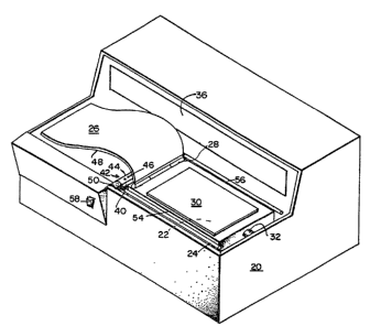
Referring now to the drawings, Figure 1 shows the
apparatus of this invention which includes a light box
housing 20, a support plate 22, a support plate frame 24 and
a phototool 26. The phototool 26 is restrained at one end
thereof by a hinge 28 and is adapced to be held in registra-
tion with a PWB 30. The support assembly ( 22 and 24) is
rotatably mounted so as to pivot about shaft 32.
The support plate 22 can have holes or slots (not
shown) through which vacuum can be applied to the und~rside
of the PWB 30 to hold it s~curely in place a~ainst the
support plate 22 during exposu~e, the polymer ~uring step.
A vacuum source can be connected to the support assembly ( 22
and 24~ through the shaft 32.
Although the hinge 28 can be permanently attached to
the support plate frame 24, preferably, it is mounted
thereto by means of screws and screw slots (both not shown~
in a conventional manner so that screw slots (not shown) in
the support plate frame 24 lay at right angles to screw
slots in the hinge 28. In this way, the hinge 28 can be
moved in two directions to permit accurate alignment or
registration of the phototool 26 with the P~B 30 on the
support plate 22.
Phototool 26 and PWB 30 are coated with photosensitive
poly~er 34 by s_reen printing to the desired thickness. A
coating assembly can be moullted in a compartment 36 of the
light box housing 20, and it can be comprised of a container
for photopolymer, an outlet port and metering means to
control the flow rate of photopolymer, and a doctor blade
-12- 1420
.
positioned behind the photopolymer outlet. The coating
assembly can be mounted on its own ~raverse rod, extending
across the length of the co,mpartment 36. Wh~n the phototool
26 and PWB 30 have been properly positionet in place, the
coating assembly circuit is energized. The compartment door
rolls up and inward and the coating assembly moves out over
the phototool and PWB. As the assembly moves along the
phototool and/or PWB, photopolymer is metered onto either
one or both of them and is smoothed out by the following
doctor blade. At the end of the coating cycle a limit
switch is activated to return the coating assembly back
along its traverse rod and into the compartment 36.
The photosensitive polymer can be partially cured, if
desired, by pre-exposure to actinic light before the photo~
tool is placed in registration with the PWB. Optionally,
the phototool need not be coated with the photosensitive
polymer.
In prior art methods of registering a phototool onto a
PWB, a doctor knife or roller would be used to urge the
2Q unrestrained phototool against the photopolymer coated PWB.
This resulted in air entrapment, as well as wrinkling and
stretching of the phototool, causing the phototoo~ to be out
of registration with the PWB. Furthermore, the phototool is
easily scratched by the doctor knife. In so~e cases all of
these faults could occur together.
To avoid these disadvantages of prior art application
techniques, the phototool 26 is applied to the PWB 30 by use
of a roller 40 while simultaneously tensioning the photo~ool
26 with a restraining means 42 adjacent the roller 40
Presently, it is contemplated that the restraining means 42
is comprised of a hollo~ed chamber 44 with pcrts 46 to
permit evacuation of air wi~hin the chamber 44 for the
purpose of exerting a suction force upon an outside surface
48 of the phototool 26 to urge the phototool 26 against the
$
-13- 142~
res~raining mean~ 42. At least one surface of the restrain-
in~ mean~ 42 is maintained in ~}iding contact with the
phototool 26, preferably along a smooth curve, to minimize
scratching the phototool 26 and to ensure uniform suction
force to overcome natural tension (bowing) in the ~lexible
phototool.
Referring now to Figures 1, 2 and 3, the roller 40 and
restraining means 42 are mounted on supports 50, 52. The
supports 50, 52 are movably mounted on traverse rods 54, 56,
respectively, so that as they move along the traverse rods
in the direction of the arrow (Figure 3), the phototool 26
is urged against the PWB 30 by the roller 40. At the same
time, the phototool 26 is restrained by the suction force
exerted by tbe restraining means 42 causing the phototool 26
to be urged against the chamber 44. The result is that the
phototool 26 is under a slight tension and is gently pulled
off the chamber 44 as the roller 4U is advanced.
Consequently, the phototool is laid down wrinkle free,
and all air which would otherwise be entrapped between the
phototool and the PWB is squeegeed out by the roller. No
misalignment occurs because there is no stretching of the
phototool in the process of laying it down against ~he PWB.
After the phototool 26 has been applied to the PWB 30,
the supports 50, 52 are retracted and the support plate 22
with the PWB 30 and phototool 26 in place can now be pivoted
abou~ shaft 32 for exposure by UV lamps situated within the
light box housing 20 immediately below the support plate 22.
Alternately, a portable light source can be used to activate
the photosensitive polymer. The light box housing ~0 can be
equi~p~d with a manl~al s~itch 58 for energizing the lamps.
Preferably, shaft 32 is restrained so that it can turn
only through 180 degrees. The restraining means (not shown~
can be a cam rigidly mounted to the shaft 32. As the
support assembly ( 22 and 24) rotates through 180 de~rees,
-14- 142~
ehe cam strikes a stop (not shown3 which restrains further
motion. A pressure activated light switch (not shown) can
be mounted on the stop to automatically activate a li~ht
switch to energize the lamps, Similarly, the cam can strike
a stop when it is reversed through 180 degrees to its
original position. This latter stop can serve to m intain
the support plate 22 in a stable position while the photo-
tool 26 is being urged against the PWB 30.
The supports 50, 52 can be moved by a drive means (not
shown) which can be a belt or chain drive advanced by a
reversible motor,
In ano~her embodiment, the traverse rods 54, 56 can be
threaded and the supports 50, 52 are advanced by rotating
t~e tr~verse rods 54, 56, each traverse rod 54, 56 being
threaded into a support 50, 52, respectively,
As shown in Figures 4 and 5, roller 40 and restraining
means 42 are mounted so as to be capable of being raised and
lowered. In the lower position, the phototool 26 can be
laid flat against the light box housing 20 for coating with
photosensitive polymer 34, The raising and lowering of the
roller 40 and restraining means 42 is accomplished by moving
the traverse rods 54, 56 and supports 50, 52 as a unit, In
the upper position, the roller 40 and restraining m~ans 42
are advanced to apply the phototool 26 to the PWB 30 in a
controlled manner as shown in Figures 5, 6 and 7,
As used in the specification and claims, the term
photopolymer means a polymer which, when exposed to actinic
light, will be cured or crosslinked. T~e term light sensi-
tive receiving element includes a photopolymer coated
substrate. The substrate can be a printed circuit board, a
printing plate, or other surface upon which an image is to
be transferred,
Although a preferred embodiment of the present inven-
tion has been shown and àescribed in detail, various
-15- 1420
modifications and alternative embodiments of the invention
will now be apparent to those skilled in the art and such
changes are considexed to be within the spirit and scope of
the invention.