Note: Descriptions are shown in the official language in which they were submitted.
8~
--1--
OPEN CYCLE COOL~NG O~ ELECTRICAL CIRCUITS
BACKGROUND OF THE INVENTION
1. Field of the Invention
The invention relates to apparatus for operating low
temperature electronic devices, and more particularly,
for cooling such devices to the necessary temperature.
2. Description of Related Art
In order to use superconducting technologies to measure
electrical waveforms produced by roo~ temperature
devices, or indeed to interface any low temperature
electronic device to a room temperature electronic
device, an interface scheme must be found which
satisfies the electrical, mechanical, and temperature
constraints discussed below:
Electrical Constraints. when operating at high
frequencies and extremely short pulse durations, any
power lost in the transmission line between the low
temperature circuit and the room temperature circuit
will degrade the signal transfer. This degradation
appears as pulse dispersion or pulse spreading. To
minimize 105s, the transmission lines should be made of
a low resistance material, be as short as possible, and
~2~3S~
have the largest possible cross sectional area. The
latter constraint is limited by the further constraint
that the width of the transmission line should not
exceed the wavelength of the maximum frequency of
interest, because larger conductors will waveguide and
cause geometric losses.
Mechanical Constraints. Since one end of the
transmission line will be operating at extremely low
temperatures and the other end will be operating at room
temperatures, it is important that the transmission line
be able to withstand that temperature difference. Thus,
the bond between the transmission line and the low
temperature device should be able to withstand that low
temperature, and the seal through which the transmission
line passes between the low temperature volume and the
room temperature volume should also be able to withstand
the necessary temperatures. These elements should also
be able to withstand repeated cycling from room
temperature to low temperature for maintenance,
replenishment of helium supply, and general everyday
use. Additionally, the temperature coefficient of
expansion of the transmission lines should closely match
that of the low temperature device, and the construction
should be such as to permit the apparatus to tolerate
vibration and temperature-induced changes in
transmission line length (collectively referred to
herein as "movement").
Temperature Constraints. In order to prevent extensive
heat transfer from the room temperature volume to the
low temperature volume, the transmission lines should be
as long as possible. This is directly contrary to the
electrical constraints which favor short transmission
lines. The transmission lines should also be made of a
material which has low thermal conductivity. Since low
thermal conductivity usually implies low electrical
~2~i9859~
conductivity, this constraint, too, is con~rary to the
electrical constraints.
Workers in the field of superconducting electronics
typically achieve the necessary temperatures by
immersing their circuits in liquid helium. See, for
example, Hamilton, "High-Speed, Low-Crosstalk Chip
Holder for Josephson Integrated Circuits," IEEE Trans.
on Instrumentation and Measurement, Vol. IM-31, pp.
129-131 (1982). The arrangement shown therein involves
attaching several coaxial cables to a Josephson Junction
chip which is to be immersed in a liquid helium dewarO
See also Hamilton et al., IEEE Transactions on
~agnetics, Vol. MAG-17, pp. 577-582 (1981), in which a
low-temperature chip is inserted partially inside a
coaxial line to couple the signals therethrough to the
room-temperature devices. Although not mentioned in the
reference, it is believed that the low-temperature chip
is then immersed in liquid helium. Both arrangements
are constrained to have large coaxial lines which have
high thermal conductivity. In order to avoid heat
losses, the lines are therefore constrained to be long.
In addition, these arrangements cannot be adapted easily
to planar chips. Furthermore, at least the latter
system is constrained to couple only one line to a chip,
which limits the system in utility.
An attempt to deal with the constraints described above
appears in U.S. Patent No. 4,498,046 to Faris. The
interface described therein includes a pass-through
~iquid-helium tight vacuum seal which consists o~ a
flange and two half cylindrical fused quartz portions,
unequal in length, which act as a pass-through plug from
a liquid-helium filled cryostat to a vacuum chamber.
Fused quartz, while thermally non-conductive, forms a
low loss dielectric substrate for conductive copper
striplines which are patterned on the flat surface of
~2~
the longer portion. The coefficient of expansion of
fused quartz is small and relatively well matched to
that of silicon, which is used for Josephson and
semiconductor chip substrates.
The two fused quartz half-cylinder portions of the
pass-through plug are arranged so that the portion with
the copper striplines extends sufficiently beyond its
mating half~cylinder portion on both ends to provide two
platforms at opposite ends of the plug. The low
temperature semiconductor chip or device is mounted on
one of these platforms and the room temperature chip or
device is mounted on the other. The cylindrical
geometry was chosen in order to minimize stress on
cement used to seal the chamber wall around the pass-
throuqh. The planar nature of the striplines allows lowinductance connections to be made directly to the two
chips which are also planar. The low inductance
contacts are copper spheres or other rigid-probes, about
100 um in diameter or smaller, which penetrate solder
pads on the chips when forced into contact by mechanical
pressure. The wall of the cryostat is sealed around the
pass-through with a thin layer o~ non-conductive cement.
In operation, the two chips are mounted on the platforms
and the pass-through is inserted through the cryostat
wall such that the low temperature chip is immersed in
liquid helium in the cryostat and the room temperature
chip is disposed inside the vacuum chamber. A heating
element and thermocouple are placed near the position of
the room temperature chip in order to warm it. This
chamber must be evacuated in order to prevent frosting
of water and other gases on the plug, and also to
provide adequate insulation for the cryostat.
The '046 apparatus has numerous problems which render it
costly, unreliable and impractical to use in most
applications. First, the only method described in the
1~6~B~
'046 patent for cooling the low temperature device
involved immersing it in liquid helium. This renders
the apparatus bulky and cumbersome.
Second, the apparatus requires at least two seals, one
between the cryostat and the vacuum chamber, and one
between the vacuum chamber and the external environment.
At least the first o these seals is extremely difficult
to create, because it must operate at cryogenic
temperatures, must be able to be cycled many times
between cryogenic and room temperatures, and must be
able to withstand a certain amount of vibration without
breaking. Due to the small size of the helium atom, it
can pass through extremely small cracks in the seal and
can even pass through most materials which are not
cracked. This severely limits the types of seals which
can be used.
Third, since the low temperature chip is fabricated on a
silicon substrate and the transmission line is
fabricated on a fused quartz substrate, the two elements
must usually be made separately and then mechanically
and electrically bonded together. These additional
steps are costly. In addition, even though their
respective temperature coefficients of expansion are
close, the mere fact that the materials are different
requires some mismatch which degrades the electrical
connection and the mechanical reliability of the bond.
Fourth, because multiple sealed layers of chambers and
insulating material are required, the transmission line
which carries electrical signals between the two chips
must be very long.
Fifth, the pass-through of the '046 apparatus has to be
cylindrical in order to obtain a good seal. ~his
renders it difficult to manufacture, and requ.ires
3859~
--6--
special geometries such as that shown in Fig. 3E of the
'046 patent.
Finally, the chips used in the '046 apparatus cannot be
easily plugged in or out in order to change them.
As the above examples suggest, the field of low
temperature electronics appears to suffer from a
presumption that immersion in liquid helium is the only
feasible method of achieving the necessary temperatures.
In the field of optics, devices are sometimes cooled
using a product known by the trademark Heli-Tran, made
by Air Products and Chemicals, Allentown, PA. The
Heli-Tran comprises a vacuum enclosed mounting head for
holding the sample to be cooled, and a multi-channel
flexible transfer tube for connecting the mounting head
to a dewar of liquid helium. Although the construction
of the transfer tube is not entirely clear, it is
believed to comprise a forward helium flow capillary
(from the dewar to the mounting head), a shield tube
surrounding the forward helium flow capillary, and a
separate return flow capillary for the shield flu.id.
When the dewar is pressurized, liquid helium flows
through both the forward helium flow capillary and the
shield tube into the mounting head. The helium in the
capillary strikes the inside surface of a metal block
closin~ off the end of the transfer tube, then enters a
passage coaxially ~urrounding al1 the transfer tube
elements, travels a short distance in the return
direction, and exits through a helium exhaust port. The
helium in the shield tube turns back before the metal
block, enters the return flow capillary, and exit~ from
a shield flow return port near the dewar. The sample
holder is attached to the outside of the metal block, so
that it can conduct heat from the sample to be cooled
into the metal block, which is itself cooled by the
helium in the forward flow capillary.
A primary drawback with the Heli-Tran system is that the
mounting head is entirely enclosed in a vacuum shroud,
rendering sample demounting difficult and cumbersome.
This drawback is accentuated by the large number of
small parts associated with the mounting head which must
be removed and reinstalled when a sample is replaced.
Additionally, with respect to low temperature electronic
circuits specifically, the me~al block and sample holder
are typically much larger than the circuit itself. A
significant amount of helium is therefore consumed for
cooling thermal mass which does not itself need to be
cold. Moreover, the literature teaches total immersion
of a superconducting electronic circuit even in
combination with the Heli-Tran system or an apparent
variation thereof. In U.S. Patent NoO 3,894,403 to
Long~worth, Fig. 5, such a system is shown cooling a
liquid helium bath in which a superconducting magnet is
totally immersed.
Since total immersion structures make little or no
effort to limit the immersed surface area, the
consumption of liquid helium typically is very large.
The present invention derives in part from the
observation that the consumption of li~uid helium can be
significantly reduced if only the region in which the
low temperature circuit is located is cooled.
SUMMARY OE THE INVENTION
It is an object of the present invention to provide a
method and apparatus for cooling a low temperature
circuit.
It is another object of the invention to provide a
method and apparatus for cooling such a circuit which
does not require enclosure of the circuit in a vacuum
chamber.
~a- 61293-156
It is another object of the invention to provide a
method and apparatus for cooling such a circuit with reduced
liquid helium consumptionO
It is another object of the invention to provide a
method and apparatus for cooling such a circuit which does not
require immersion of the circuit in a bath of liquid helium.
It is another object of the invention to provide a
method and apparatus for cooling such a circuit by ejecting a
cold fluid onto the circuit and venting waste fluid to the
surrounding environment.
The above objects and others are achieved according to
the invention by directing a stream of cold fluid onto the
region of the chip substrate which contains the low temperature
circuit, and subsequently allowing the fluid to dissipate into
the surrounding environmentO The apparatus may include an
enclosure for holding the circuit, means for guiding the fluid
onto another portion of the substrate a-fter it strikes the
circuit, and/or means for directing the exit flow of the fluid
so as to cool a radiation shield which surrounds the circuit.
The exit path for the 1uid may also fold back paqt the circuit
so as to help convect out heat which enters the vicinity
radially from the outside. The circuit may be cooled directly
by directing the stream of cold fluid onto the circuit itself,
or indirectly by directing the stream of cold fluid through a
thermally conductive block, the block having a small surface
thermally connectable to the circuit.
In accordance with the present invention, there is
provided a method for localized cooling of a device containing a
low temperature region, comprising the steps of: (a) confining
said low temperature region of said device in a housing which is
` -~a- ~1293-156
open to the surrounding environment and which permits said low
temperature region to be operably connected to a second device
disposed outside the housing; (b) carrying a cooling -fluid from
a cooling fluid source and directing a stream of the cooling
fluid into the housing in the vicinity of said low temperature
region so that the cooling fluid makes thermal contact with said
low temperature region; and (c) venting the cooling fluid away
from the vicinity of said low temperature region of said device
and into the surrounding environment.
In accordance with the present invention, there is
further provided apparatus for cooling a device, comprising:
(a) an enclosure which at a first end of its length demountably
holds said device in such a manner that only a portion of said
device to be cooled is disposed within the enclosure, said
enclosure being in communication with open air and being
configured to permit the portion of said device to be cooled to
be operably connected to a second device disposed outside said
enclosure; and (b) means for carrying a cooling fluid from a
cooling fluid source and for directing the cooling fluid into
the enclosure toward the portion of said device to be cooled so
that the cooling fluid makes thermal contact with the portion of
said device to be cooled and then vents into the open air, said
means for carrying and directing being adapted to loosely fit
within an open section of the enclosure.
In accordance with the present invention, there is
further provided apparatus for cooling a device having a high
temperature and a low temperature region, comprising: (a) an
enclosure which at a first end of its length demountably holds
said device in such a manner that only said low temperature
region is disposed within the enclosure, said enclosure being in
s~
~8b- 61293-156
communication with open air and being con~igured to permit said
low temperature region to be operably connected to said high
temperature region disposed outside said enclosure; and (b)
means for carrying a cooling fluid from a cooling fluid source
and for directing the cooling fluid into the enclosure toward
said low temperature region so that the cooling fluid makes
thermal contact with said low temperature region and then
dissipates into the open air after contacting said low temper-
ature region, said means for carrying and directing being
adapted to loosely fit within an open section of the enclosure.
In accordance with the present invention, there is
further provided apparatus for locali~ed cooling of a low tem-
perature region of a device, comprising: (a) means for housing
said low temperature region in such a manner to permit said low
temperature region to be operably connected to a second device
disposed outside the means for housing, said means for housing
being in communication with open air; (b) means for carrying a
cooling fluid from a cooling fluid source and Eor directing the
cooling fluid into the means for housing in the vicinity of said
low temperature region of said device so that the cooling fluid
makes thermal contact with said low temperature region; and (c)
means for venting the cooling fluid from the vicinity of said
low-temperature region of said device to the open air.
BRIEF DESCRIPTIO~ OF THE DRAWINGS
. _
~he invention will be described with respect to
particular embodiments thereof. Reference may be made
8~
to the drawings, in which like elements are designated
by like numerals, and in which Figs. 1-7 schematically
depict cross~sectional views of various embodiments of
the present invention.
5 DETAILED DESCRIPTION
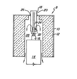
In Fig. 1 there is shown an apparatus constructed
according to the invention. A chip holder assembly 8
comprises a rigid frame 10 in the shape of an inverted
cup, the interior of which forms an open chamber 28
A lo lined with insulation 12 such as teflon or styrofoam. A
transfer tube 14 is connected to a dewar (not shown) of
cold fluid, such as liquid helium, and the inside
surface of the insulation 12 is shaped so as to loosely
fit over the free end of the transfer tube 14. The
transfer tube 14 is made up of two coaxial portions, the
inside portion for carrying the cold fluid and the
outside portion for insulating the inside portion. The
free end of the inside coaxial portion forms a nozzle 16
which need not be any particular shape, and may be
merely the cut off end of the tube. A slit is cut into
the end of the frame 10 and insulation 12 and a chip 18
is partially inserted therein. The chip 18 consists of
a substrate 20 which may be made of fused quartz; a low
temperature circuit 22 is fabricated in a known manner
on the substrate at the end thereof which is inside the
cup; and transmission lines 24 extendiny from the
circuit 22 longitudinally on the substrate 20 to the
outside of the cup. The low temperature circuit 22 may
be a niobium-based ~osephson junction circuit and the
transmission lines 24 may also be fabricated with
niobium. Fused quartz is chosen for the substrate
material because of its low thermal conductivity. If
desired, the slit in the end of the frame 10 may be
sealed around the chip 18 with a bead 26 of glue.
7~1o~ lal~ k
- ~L2~
--10--
When the liquid helium flow is turned on, a cold
liquid-gas mixture is ejected from the nozzle 16 and
fills the open chamber 28. The low temperature circuit
22 is thereby cooled to cryogenic temperatures within a
matter of seconds. The chip holder 8 should be oriented
so that fluid ejected from the nozzle 16 will strike the
chip lB end-on, but exact alignment is not critical.
The apparatus should operate success~ully even if the
stream of fluid misses the chip, as long as venting of
the waste fluid is sufficiently slow to cause backed-up
fluid to make thermal contact therewith. Waste gas
leaves the chamber 28 through a space between the
transfer tube 14 and the insulation 12. A second
circuit (not shown), operable at a different temperature
such as room temperature, may be fabricated directly on
the portion of the substrate 20 which is outside the
frame 10, or may be connected to the transmission lines
24 via wires (not shown) bonded thereto.
The advantages of this construction are apparent.
First, the apparatus is extremely easy and inexpensive
to construct, and its small size permits the use of
short transmission lines. No critical seals are
required because the entire apparatus can be operated in
open air without a vacuum shroud. Additionally, since
the radiative area of the sample being cooled is so
small, the consumption of liquid helium over that of
prior art methods is significantly reduced. Finally~
the sample is easily demountable by replacing the chip
in the chip holder assembly or by simply replacing the
entire assembly. It should be noted that the above-
described apparatus can be used to cool any sample of
any shape, whether or not electronic in nature. If the
sample extends outside the cooling chamber as does the
sample in Fig. 1, however, then it is desirable that the
sample have low thermal conductivity.
~L~6~
In Fig. 2 there is shown another embodiment of the
present invention similar to that shown in Fig. 1
wherein a cylindrical guide 40, which may be made of an
insulating material, has been inserted in the chamber 28
around the chip 18. The guide 40 is so disposed as to
help direct the flow of fluid from the nozzle 16 onto
the circuit 22, and to keep the fluid in thermal contact
with other parts of the chip 18 after it cools the
circuit. This helps reduce heat conduction along the
length of the substrate 20. The guide 40 is spaced from
the inside wall of the insulation 12, so that fluid
which emerges from the nozzle 16 can flow over the top
- of the guide and out of the chamber 28 by passing
through the space between the guide 40 and the
insulation 12 and then between-the transfer tube 14 and
the insulation 12. The guide 40 is held in place by
means (not shown) which permits such flow of the fluid.
The addition of the guide 40 provides the additional
advantage that waste fluid, as it folds back past the
circuit 22, helps convect out of the chamber 28 heat
which has penetrated the insulation 12 radially from the
external environment. Moreover, the quide 40 or the
inside surface of insulation 12 may be made of or coated
with a material to act as a radiation shield. In that
case the waste fluid will help cool the shield and make
its operation more effective.
An embodiment of the present invention which capitalizes
on the latter feature is shown in Fig. 3. A labyrinth
50 is constructed with a series of four alternately
inverted cups 52, 54, 56 and 58, concentrically
disposed. That is, the outer cup 52 of the labyrinth 50
opens downward; the next inner cup 54 is disposed
coaxially with and inside cup 52 and opens upward; the
next cup 56 is disposed coaxially with and inside cup 54
and opens downward; and the innermost cup 58 is disposed
coaxially with and inside the cup 56 and opens upward.
~6~3~3S~
Although the terms upward and downward are used in this
description, it will be understood that the labyrinth 50
will operate in any orientation, including horizontally.
Also, although four cups have been shown in the figure,
it will be understood that any number of cups may be
used.
The rim and walls of each cup are spaced from the floor
and walls, respectively, of each adjacent cup, so as to
provide a convoluted passage from the interior of the
inside cup 5~ to the external environment. The floors
of ~he two downward opening cups S2 and 56 contain slits
60 and 64, respectively. The chip 18 is inserted
through the slits 60 and 64 so that the end on which the
low temperature circuit is fabricated is disposed inside
the cup 58, and the opposite end of the chip 18 is
disposed outside the labyrinth 50. The two upward
opening cups 54 and 58 also contain holes in their
floors, which holes are designated 62 and 66,
respectively. The nozzle 16 passes through the holes 62
and 66 so as to open into the inside of cup 58. As in
previously described embodiments, the nozzle }6 and the
chip 18 should be oriented so that fluid ejected from
the nozzle 16 will strike the chip 18 end-on, but
alignment is not critical.
In operation, a cold fluid ejected from the nozzle 16
will strike the end of the chip 18 and cool it quickly
to cryogenic temperatures. Because of the torturous
nature of the path from the inside of cup 58 to the
external environment, greater fluid pressure may be
required to maintain the desired temperatures near the
chip 18. Much of the heat which enters the labyrinth 50
radially, however, will be largely convected out of each
successive layer by the moving fluid. The cups 52, 54,
56 and 58 may be made of any material, but a rigid,
thermally resistive material such as teflon is
~ ~rad~ r~
5fl~
-13-
preferred. Construction is extremely simple and
inexpensive, and the labyrinth 50 may be made as small
as desired.
The principle of the present invention may also be used
in accordance with the embodiment shown in Fig. 4. In
this embodiment, a cover 82 rests on top of an upright
styrofoam cup 80. The styrofoam cup 80 has a vent hole
34 in its wall, near the cover 82r for venting waste
cooling fluid. The liquid helium transfer tube 14 is
disposed beneath the cup 80, the nozzle 16 passing
through the floor of the cup 80 and opening vertically
upward into the interior thereof. Held horizontally in
place above the nozzle 16 by means not shown is a quartz
wafer 86, on the underside of which a low temperature
circuit 88 is fabricated. The low temperature circuit
B8 is extremely small~ and only that portion of the
wafer need be disposed above the nozzle 16. Connection
wires 90 are bonded to the wafer, making electrical
connection with the low temperature circuit 88, and pass
through the wall of the cup 80 to the external
environment. When liquid helium Elows through the
transfer tube 14, it quickly cools the low temperature
circuit 88 to cryogenic temperatures. Waste fluid forms
a cloud inside the cup 80, reducing heat pickup through
the walls of the cup 80 from the external environment,
and then exits the cup 80 through the vent 84.
The embodiment in Fig. 4 is especially useful for wafer
probing, which involves testing of a low temperature
circuit fabricated with many others on the same
substrate, later to be cut apartO It should be noted
that the embodiment will also operate successfully if
the wafer B6 is inverted, i.e~, with the low temperature
circuits located on the top side thereof, if the quartz
substrate is thin enough. Additionally, and this is
applicable to many embodiments, if the low temperature
85~
-I4-
circuit 88 is a type which does not require temperatures
as low as that obtainable through direct bombardment
with liquid helium, somewhat higher temperatures may be
obtained by pulsing the helium supply vr by supplying
helium at reduced flow rates. Under such circumstances
it is advisable to insert a block having some thermal
mass between the nozzle 16 and the wafer 86 to help
stabilize the temperature.
The embodiment shown in Fig 5 is also useful for wafer
probing. In this embodiment, the liquid helium from the
transfer tube 14 strikes the low temperature circuit 88
from above, and probes 100 and 102 make electrical
contact with connection pads (not shown) on the circuit.
A styrofoam disc 104 may be pressed up against the
underside of the wafer 86 to help insulate the circuit
88. Alternatively, another transfer tube such as 14 may
direct liquid helium to the underside of the wafer B6
under the circuit 88 in place of the styrofoam disc 104.
If the apparatus (or indeed any apparatus made in
accordance with the invention) is disposed in ordinar~
air, the extreme cold of the liquid helium will cause
ice to build up around the nozzle, Such ice consists
mostly of 2~ C2 and N2. This is not necessarily
detrimental, because the ice acts as an insulator. It
also evaporates within a short time after the liquid
helium is turned off. If desired, however, the ice may
be prevented by enclosinq the entire apparatus in a
container which is effectively closed on its top and
sides but contains openings below the level of the
circuit. In this way gaseous helium will be caught in
the container, gradually filling it from top to bottom
until the gases which would otherwise freeze have all
been forced out the bottom openings.
Fig. 6 shows an embodiment of the present invention in
35~
-15-
which a low temperature circuit is indirectly, rather
than direc~ly, cooled by flowing liquid helium. In this
embodiment, an aluminum block 110 having a number of
channels 112 drilled therethrough is fitted over the end
of the nozzle 16. The channels 112 are oriented in such
a manner that liquid helium ejected from the nozzle 16
will be directed through the channels 112 and will cool
the block 110 relatively evenly. The block 110 and the
end of transfer tube 14 may be surrounded by an
insulator such as styrofoam block 114, in which case the
channels 112 continue through the styrofoam to the
external environment. The aluminum block 110 has an
exposed flat surface 116 which is slightly larger than
the low temperature circuit 88 to be cooled. The
smaller this surface, the less liquid helium will be
expended to cool regions of the sample which do not need
to be maintained at such low temperatures. On the other
hand, the surface 116 may be made slightly larger than
the circuit 88 to aid in alignment and also to help draw
2~ off heat being conducted along the substrate before it
reaches the circuit. The wafer 86 with the low
temperature circuit 88 on its underside is pressed
against tAe surface 116 so that the low temperature
circuit 88 is in thermal communication therewithO Heat
sink compound 118 may be used to improve this
connection. As in previously described embodiments, the
wafer 86 may be backed by a styrofoam block 120.
Fig. 7 shows a coolant transfer line, designated
generally as 140, which terminates in a mounting head,
designated generally as 142, all in accordance with the
present invention. The transfer line 140 is quadaxial,
consisting of a coolant flow conduit 144 (referred to
herein as a capillary) in the center, surrounded by an
inner vacuum jacket 146, surrounded in turn by an
annular coolant return passage 148, all enclosed in an
outer vacuum jacket 150. The coolant flow capillary 144
~ -16-
extends slightly beyond the end of inner ~acuum jacket
146, and the outer vacuum jacket 150 extends
significantly beyond the capillary 144. Spacers 152 are
disposed in the coolant return passage 148 to maintain a
relatively constant spacing between the vacuum jackets
146 and 150 without blocking coolant return flow. At
the opposite end of the transfer line 140, not shown, a
capillary connects the two vacuum jackets 146 and ;50
together and a valved port is provided for connection to
an external vacuum pump.
A styrofoam guide cylinder 156, similiar to the guide 40
in Fig. 2, is disposed coaxially with and attached to
the end of the capillary 144 and inner vacuum jacket
146. The inside surface of th.e end oE the guide 156
adjacent to the capillary 144 and jacket 146 is stepped,
so that the end of the guide 156 is wide enough to fit
over the vacuum jacket 146 but the remainder of the
guide 156 is wide enough to fit over only the capillary
144. The capillary 144 extends a short distance inside
the guide 156, and the guide 156 is short enough that it
terminates short of the end of the outer vacuum jacket
150.
Fitted tightly over the end of the transfer l.ine 140,
and outside the outer vacuum jacket 150, is a styrofoam
cap 158 with a slit 160 in its end. A metal cap 162
with its own slit 164, alignable with the slit 160 in
the styrofoam cap, is adapted to fit over the styrofoam
cap 158. The walls of the styrofoam cap 158 extend down
beyond the lower end of the guide cylinder 156,
encircling it along its entize length, and the walls of
the metal cap 162 extend farther down still. In the
annular space formed between the outer vacuum jacket 150
and the walls of the metal cap 162, and below the end of
the styrofoam cap 158, there is metal rin~ 166 attached
to the vacuum jacket 150 and encircled by a compressible
1~ 5~
-17-
O-ring 168. This structure helps seal the end of the
transfer line 140 when the metal cap 162 is in place. A
small heater coil 170 encircles the outside of the
transfer line 140 below the ring 166 in order to prevent
icing outside the mounting head 142. The slits 160 and
164 in the end of the styrofoam cap 158 and the metal
cap 162, respectively, are alignable and adapted to
accept the chip 18 discussed previously. The chip 18 is
shown in Fig. 7 in edge view only, inserted in the slits
and disposed such that its low temperature end is .inside
the guide cylinder 156 and its room temperature end is
exposed outside the mounting head 142. The room
temperature end is mounted on one face of a small metal
block 172 attached to the outside of the metal cap 162
adjacent to the slit 164. The slit 164 may also be
sealed around the chip 18.
In use, the styrofoam cap 158 remains attached to the
end of the transfer line 140, and the metal cap 162, the
block 172 and the chip 18 form a unit which may be
easily removed and interchanged with other units
assembled in the same way. Once the unit is in place,
the low temperature circuit on the chip 18 may be cooled
to cryogenic temperatures within a few seconds by
turning on the flow of liquid helium. No vacuum pumping
is needed since the vacuum jackets 146 and 150, which
never need to be exposed to air, can retain their vacuum
for long periods of time.
It should be apparent that the structure of Fig. 7 also
takes advantage of the features of Fig. 2 in that waste
helium which has done its work on the low temperature
circuit near the lower end of the chip 18 is then guided
along the surfaces of the chip by the guide 156 where it
helps counter heat conduction along the chip from the
outside. The waste helium then flows down the outside
of the guide 156 and helps convect out heat which has
5~
-18-
entered the vicinity radially This process continues
down the length of the quadaxial tube 140 to reduce
radially directed heating of the helium in the capillary
144. Additionally, the guide 156 and/or the outer wall
of the inner vacuum jacket 146 may be made of or coated
wi~h a radia~ion shield which will be cooled by the
waste helium. Moreover, since the capillary 144 is so
well insulated inside the quadaxial transfer line 140,
the line 140 can be made relatively longer in order to
reduce heat conduction axially along the various members
thereof.
The invention has been described with respect to
particular embodiments thereof, and one skilled in the
art can now easily ascertain its essential
characteristics. Numerous changes and modifications are
possible to adapt it to various usages and conditions,
all within the scope of the invention. ~or example,
wherever an insulator such as styrofoam is shown,
another insulating material or even a vacuum jacket may
be used. Radiation shields may be used at various
locations in the various embodiments to help reduce
liquid helium consumption. ~dditionally, embodiments of
the invention may be disposed on the end of a flexible
transfer tube for cold fluid such that it may be used as
a probe. This might be useful, for example, in certain
biomedical applications where the low temperature
circuit comprises a "squid". The person of ordinary
skill in the art can easily adapt the principles of the
present invention to these and many other situations.