Note: Descriptions are shown in the official language in which they were submitted.
3~
~ .
ENCAPSULATED LIQUID CRYSTAL HAVING A SMECTIC PHASE
TECHNICAL FIELD
The present inventlon relates generally to liquid
crystals and, more particularly, to encapsulated
liquid crystals having a smectic phase. Moreover, the
invention relates to devices using such encapsulated
liquid crystals and to methods of making such encapsu-
lated liquid crystals and devices.
BACKGROUND
Liquid crys als currently are used in a wide variety
of devices, including optical devices such as visual
displays. Such devices usually require relatively low
power and have a satisfactory response time, provide
reasonable contrast, and are relatively economical.
The propertv of liquid crystals enabling use, for
example, in visual displays, is the ability of liquid
crystals to transmit light on one hand, and to scatter
and/or absorb light, on the other, depending on the
alignment (or lack of alignment) of the liquid crystal
structure with, e.g., an electric field applied across
the liquid crystal material. An example of elec-
trically responsive liquid crystal material and use
thereof is provided in U.S. Patent 3,322,485.
,, . -( . :
, ;,, ",~ ~ ,.~
: ` ; . '
. .
12~3~ ~
--2--
Certain liquid crystal material is responsive to
temperature, changing optical characteristics in
response to temperature of the liquid crystal mate-
rial.
The present invention is disclosed hereinafter parti-
cularly with reference to the use of liquid crystal
material that is particularly responsive to an elec-
tric field as well as to temperature.
Currently there are three categories of liquid crystal
materials, namely cholesteric, nematic and smectic
types. The invention of the present application
relates in the preferred embodiment described below to
use of liquid crystal material having a smectic phase.
The invention may also be employed with a liquid
crystal material having a smectic as well as a nematic
phase.
The various characteristics of the cholesteric,
nematic and smectic types of liquid crystal material
are described in the prior art. One know charactex-
istic of liquid crystal material is that of reversi-
bility; in particular it is noted here that nematic
liquid crystal material is known to be reversible, but
cholesteric material is not reversible. One charac-
teristic of a reversible nematic material is that the
liquid crystal structure will return to its original
configuration after an electric field, for example,
has been applied and then removed. On the other hand,
smectic material will retain its configuration even
after removal of an electric field.
To enhance contrast and possibly other properties of
liquid crystal material, pleochroic dyes have been
mixed with the liquid crystal material to form a
,~
;:
~:
,,; ' .
~;27~7
--3--
solution therewith. The molecules of the pleochroic
dye generally allgn with the molecules of the liquid
crystal material. Therefore, such pleochroic dyes
will tend to function optically in a manner similar to
that of the liquld crystal material in response to a
changing parameter, such as application or non-appli-
cation of an electric field or heat. Examples of the
use of pleochroic dyes with liquid crystal material
are described in U.S. Patents 3,499,702 and 3,551,026.
An important characteristic of liquid crystal material
is anisotropy. An anisotropic material has different
physical properties in different directions. For
example, liquid crystals are optically anisotropic,
i.e., they have indices of refraction which vary with
the direction of propagation and polarization of the
incident light.
Liquid crystal material also has electrical aniso-
tropy. For example, the dielectric constant for
smectic liquid crystal material may be one value when
the molecules in the liquid crystal structure are
parallel to the electric field and may have a differ-
ent value when the molecules in the liquid crystal
structure are aligned perpendicular to an electric
field. Since such dielectric value is a function of
alignment, for example, reference to the same as a
"dielectric coefficient" may be more apt than the
usual "dielectric constant" label. Similar properties
are true for other types of liquid crystals.
Some brief discussion of the encapsulation of choles-
teric liquid crystal material is presented in U.S.
Patents 3,720,623, 3,341,466, and 2,800,457, the
latter two patents being referred to in the first
named patent.
3L27g~
In the past, devices using liquid crystals, such as
visual display devices or other devices, have been of
relatively small size. Large size devices using
liquid crystals, such as, for example, a billboard
display or a sign have not been satisfactorily fabri-
catable for a number of reasons. One reason is the
fluidity of the liquid crystals, (the liquid crystal
material may tend to flow creating areas of the
display that have different thicknesses). ~s a
result, the optical characteristics of the display may
lack uniformity, have varying contrast characteristics
at different portions of the display, etc. The
thickness variations in turn cause variations or
gradations in optical properties of the liquid crystal
device. Moreover, the varying thickness of the liquid
crystal layer will cause corresponding variations in
the electrical properties of the liquid crystal layer,
such as capacitance and impe~dance, further reducing
uniformity of a large size liquid crystal device. The
varying electrical properties of the liquid crystal
layer, then, also may cause a corresponding variation
in the effective electric field applied across the
liquid crystal material and/or in response to a
constant electric field would respond differently at
areas of the liquid crystal that are of different
thicknesses.
A pleochroic display, i.e., one in which pleochroic
dye and liquid crystal material are in solution
together, has the advantage of not requiring the use
of a polarizer. However, such a pleochroic device has
a disadvantage of relatively low contrast when only
nematic liquid crystal material is used. It was
discovered in the past, though, that a cholesteric
liquid crystal material could be added to the nematic
one together with the dye to improve the contrast
,..
':
ratio. See White et al. article, ournal of Applied
Physics, Volume 45, No. 11, Novembex 1974, at pages
4718-4723, for example. The cholesteric material
would tend not to return to its original zero field
form when the electric field is removed~
Another problem encountered with pleochroic dye
included in solution with liquid crystal material,
regardless of the particular type of liquid crystal
material, is that the light absorption of the dye is
not zero in the "field-on" condition. Rather such
absorption in the "field-on" condition follows a
so-called ordering parameter, which relates to or is a
function of the relative alignment of the dyes. The
optical transmission characteristic of liquid cxystal
material is an exponential function of the thickness
of the liquid crystal material. Specifically, the
"on" state or "field-on" or "energiæed" state of the
liquid crystal material is an exponential function of
the thickness of the liquid crystal material, and the
"absorbing" state or "field-off" state also is a
different exponential function of the thickness.
To overcome those problems described in the two
immediately preceding paragraphs, the liquid crystal
material should have an optimum uniform thickness.
(As used herein the term "liquid crystal" material
means the liquid crystals themselves and, depending on
context, the pleochroic dye in solution therewith).
There also should be an optimum spacing of the elec-
trodes by which the electric field or heat is applied
to the liquid crystal material. To maintain such
optimum thickness and spacing, rather close tolerances
must be maintained. To maintain close tolerances,
there is a limit as to the size of the device using
such liquid crystals, for it is quite difficult to
~ 2~3~
-6- 51051-lg74
maintain close tolerances over large surface areas~ for example.
BRIEF SUMMARY_OF TH~ INVl~NTION
Brie~ly, according to one aspec~ of ~he invention,
liquid crystal ma~erial having a smectic phase is encapsulated.
According to another aspect, the encapsulated liquid crystal
material is used in liquid crystal d&vices, such as visual display
devlces and optical shutters. And according to fur~her aspects
thexe are provided methods for encapsulating liquid crys~tal
material and for making a liquid crystal device using such
encapsulated liquid crystal material.
Thus, according to one aspect, the present invention
provides liquid crystal apparatus, aomprising liquid crystal
matsrial havlng a smectic phase, and encapsulating medium means
for confining said liquid crystal material in discrete volumes,
said encapsula~ing medium means, inducing a generally distorted
alignment of said llquid crystal material which in response to
such alignment at least one of scatters and absorbs li~ht and
which in response to a prescribed input reduces the amount of such
scattering or absorption.
According to another aspect, the present invention
provides a liquid crystal apparatus, comprlsing liquid crystal
materlal having a smec$ic and a nematic phase, and encapsulating
medium means ~or confining said liquid crystal material in
discrete volumes, said encapsulating medium means inducing a
generally distorted alignment of said llquid crystal material
which in response to such alignment at least one of ~catters and
absorbs light and which in response to a prescribed lnput reduces
,.
~2~@3~
--6a-- 61051-:L~74
the amoun~ of sucll scattering or absorption.
According ~o still another a~pect, the present inverltion
provides a method of making encapsulated smectic llquid crystals,
comprisiny mixing a~ least an encapsulating medium and a liguid
crystal material haviny a smectic phase, and further comprising
causing such liquid crystal mater.ial to perform substantially
independently of the optical polarization d:irection of incident
light, including confining such liquid crystal material in a
capsule formed by such encapsulating medium that causes distortion
of the direct:ion of the liquid crystal molecules when no electric
field is applied thereto.
According to yet another aspect, the present invention
provides a method of causing a liquid crystal material having a
smectic phase to perform substantially independently of the
optical polarization direction of incident light, comprising
confining of such liquid crystal material in a capsule-like volume
which causes distortion of the direction of the liquid crystal
material to at least one of scatter and absorb light incident
thereon, and applying an electric field to at least some of such
liquid cry~tal to align the liquid crystal with respect to such
field to reduce such sca~tering or absorption.
A liquid crystal having both a smectic and nematic phase
may also be encapsulated in accordance wi~h the present invention.
The transition temperature of the liquid crystal material
determines whether it is in the smectic or nematic phase. In the
nematic phase, the liquid crystal is opera~ionally nematic, as
defined below and in U.S. Patent 4,435,047, issued March 6
,. ''. '
:
.-. .
~7~3:~
-6b-- 61051-1974
198~, in -the name of Fergason and entitled ENCAPSU1ATED LIQIJID
CRYSTAL AND M~'ThOD, by "operationally nematic" is rneant that, in
the absence of external fiel.ds, sttructural distortion of the
li~uid crystal is dominated by the orientat;ion of the liquid
crys-tal at its boundaries rather than by bulk effects, such as
very strong twis-ts (as in ~holesteri~ material) or layerincl (as in
smectic material). rrhus, for exar~ple, chiral ingredients which
induce a tendency to twi.st bu~ cannot overcome the ef~ects of
boundary alignment would still be
,,",.~,
_! 1, ....
3~7
considered operationally nematic. 5uch operationally
nematic liquid crystal matexial may include pleochroic
dyes, chiral compounds, or other co-ingredients.
A capsule as used herein generally refers to a con-
tainment device or medium that confines a quantity of
liquid crystal material, and "encapsulating medium" or
"material" is that medium or material of which such
capsules are formed. An "encapsulated liquid crystal"
or "encapsulated liquid crystal material" means a
quantity of liquid cry~tal material confined or
contained in discrete volumes within the encapsulating
medium, for example in a solid medium as individual
capsules or dried stable emulsions. The discrete
volumes, however, may also be interconnected, for
example, by one or more passages. The liquid crystal
would preferably be in both the discrete ~olumes and
interconnecting passages. Thus, the internal volumes
of respective capsules may be fluidly coupled via one
or more interconnecting passages.
Capsules according to this invention generally have an
approximately spherical configuration (though this is
not, per se, a requisite of the invention~ having a
diameter from about 0.3 to 100 microns, preferably 0.1
to 30 microns, especially 3 to 15 microns, for example
5 to 15 microns. In the context of this invention,
encapsulation and like terms refer not only to the
formation of such articles as are generally referred
to as capsules, but also to the formation of stable
emulsions or dispersons of the liquid crystal material
in an agent (an encapsulating medium) which results in
the formation of stable, prefèrably approximately
uniformly sized, particles in a uniform surrounding
medium. Techniques for encapsulation, generally
referred to as microencapsulation because of the
;~
~ :
' ', . . .
.. ': .: ~
. . ~
' ::
~27~3~7
--8--
capsule size, as well known in the art (see, e.g.,
"Microcapsule Processing and Technology" by Asa~i
Kondo, published by Marcel Dekker, Inc.) and it will
be possible for one skilled in the art, having regard
to the disclosure herein, to determine suitable
encapsulating agents and methods for liquid crystal
materials.
A liquid crystal device is a deviced formed of liquid
crystal material. In the present invention such
devices are formed of encapsulated liquid crystals
having a smectic phase capable of providing a function
of the type typically inuring to liquid crystal
material; for example, such a liquid crystal device
may be a visual display or an optical shutter that in
response to application and removal of an electric
field and heat effects a selected attenuation of
optical radiation, preferably including from far
infrared through ultraviolet wavelengths.
One method of making encapsulated liquid crystals
includes mixing together liquid crystal material
having a smectic phase and an encapsulating medium in
which the liquid crystal material will not dissolve
and permitting the formation of discrete capsules
containing the liquid crystal material.
A method of making a liquid crystal device including
such encapsulated liquid crystal includes, for example
applying such encapsulated liquid crystal material to
a substrate. Moreover, such method includes providing
means for applying an electric field and heat to the
liquid crystal material to affect a property thereof.
According to another feature of the invention a liquid
crystal material having a smectic phase in which is
~7~
-9- 61051-1974
dissolved a pleochroic dye is placed in a generall~
sph~rical capsule. In the absence of an electric
field, the capsule wall distorts khe liquid crystal
structure so it and the dye will tend to absorb light
regardless of its polarization direction. When a
suitable electric field is applied across such a
capsule, for example across an axis thereof, the
liquid crystal material will tend to align parallel to
such field causing the absorption characteristic of
such material to be reduced to one assumed when the
liquid crystal material is in the planar configura-
tion. To help assure that adequate electric field is
applied across the liquid crystal material in the
capsule, and not just across or through the encapsu-
lating medium, and, in fact, with a minimum voltage
drop across the wall thickness of the respective
capsules, the encapsulating material preferably has a
dielectric constant no less than the lower dielectric
constant of the liquid crystal material, on the one
hand, and a relatively large impedance, on the other
hand~ Ideally, the dielectric constant of the encap-
sulating medium should be close to the higher die-
lectric constant of the liquid crystal.
Contrast of a liquid crystal device employing encapsu-
lated liquid crystals ~ay be improved by selecting an
encapsulating medium that has an index of refrac~ion
that is matched to the ordinary index of refraction of
the liquid crystal ma~erial (i.e., the index of
refraction parallel to the optical axis of the crys-
tal). See, e.g. "Optics'~ by ~orn & Wolf, or "Crystals
and the Polarising Microscope" by Hartshorne &
Stewart. The encapsulating medium may be used not
only to encapsulated liquid crystal matexial but also
to adhere the capsules to a substrate for support
thereon. Alternatively, a further binding medium may
..
.
~2~3:~7
--10--
be used ~o hold the liquid crystal capsules relative
to a substrate. In the latter case, though preferably
the additional binding medium has an index of refrac-
tion which is matched to that of the encapsulating
medium for maintaining the improved contrast charac-
teristic described above. Because the index of
refraction of a material is generally strain-depen-
dent, and strain may be induced in, e.g., the encapsu-
lating medium, it may be necessary to consider Ithis
effect in matching the indices of refraction of the
liquid crystal, encapsulatin~ medium, and binding
medium, if present. Further, if iridescence is to be
avoided, it may be desirable to match the indices of
refraction over a range of wavelengths to the extent
possible, rather than at just one wavelength.
A feature of the present invention is that the mole-
cules of the liquid crystal material in the smectic
phase prior to the application of ~n electric field
thereto tend to align themselves generally perpendicu-
lar to the curved surfaces of the spherical or other-
wise curvilinear surfaced capsule. Accordingly, the
liquid crystal structure tends to be forced or dis-
torted to a specific form, generally focal conic, so
that the resulting optical characteristic of a given
capsule containing liquid crystal material is such
that substantially all light delivered thereto will be
affected, for example, scattered (when no pleochroic
dye is present) or absorbed (when pleochroic dye is
present), prior to the application of an electric
field, regardless of the polarization direction of the
incident light. Even without dye this effect can
cause scattering and thus opacity.
Another feature of the present invention is the
ability of the molecules of the smectic phase liquid
:, .:..
.., :.
~27~3~7
~ 61051-1974
crystal material to to align themselves in a direction
parallel to an electric field applied ~hereto and to
remain i~ that alignment after removal of the electric
field. When aligned in ~his manner, the liquid
crystal material reduces the amount of scattering or
absorption of light that would otherwise be present.
The subsequent application of sufficient heat to the
liquid crystal material induces the generally dis-
torted alignment of the liquid crystal material such
that light is scattered or absorbed. The temperature
at which this occurs may ~e the smec~ic to nematic
phase transition temperature or the smectic to
isotropic phase transition temperature. This conce~t
may be called hèat-to erase.
Another feature of the presènt invention relies on the
concept of a thèrmally activated display. This
display utilizes an encapsulated liquid crystal
material having both a smectic and nematic phase. The
liquid crystal is heated so that it is in the nematic
phase, and an electric field is applied thereto to
effect a visual display. The temperature of the
liquid crystal is reduced so that it is in the smectic
phase. The electric field is removed and the display
remains. The display may be erased by heating the
liquid crystal so that it is again in the nematic
phase.
Yet another feature is the ability to control the
effective thickness of the liquid crystal material
contained in a capsule by controlling the internal
diameter of ~uch capsule~ Such diameter control may
be affected by a size fractionation separation process
during the making of the encapsulated liquid crystals
using any one of a varie~y of conventional or no~el
sorting techniques as well as by controlling the
ri~3
':
~;27~
mixing process, the quantities of ingredients, and/or
the nature of the ingredients provided during mixing.
sy controlling such thickness parameter to relatively
close tolerances, then, the subsequent tolerance
requirements when the final liquid crystal device is
made using the encapsulated liquid crystals will not
be as critical as was required in the past for non-
encapsulated devices.
Moreover, a further feature of the present invention
is that there appears to be no limitation on the size
of a high quality liquid crystal device that can be
made using the encapsulated liquid crystals in accord-
ance with the present invention. More specifically,
by providing for confinement of discrete quantities of
liquid crystal material, for example, in the described
capsules, the various problems encountered in the past
that prevented the use of liquid crystal material in
large size devices are overcome, for each individual
capsule in effect can still operate as an independent
liquid crystal device. Moreover, each capsule pre-
ferably has physical properties enabling it to be
mounted in virtually any environment including one
containing a plurality of further such liquid crystal
capsules mounted to a substrate or otherwise supported
for use in response to application and removal of some
type of excitation source, such as, for example, an
electric field or heat. This feature also enables
placement of the liquid crystal material on only
selected areas of the optical device, such as in lar~e
size displays (e.g., billboardsl, optical shutters,
etc.
Important considerations in accordance with the
invention are that an encapsulating medium having
electrical properties matched in a prescribed way to
:, ,:. .,~ . :
~.
. ' `
.:
:: ~
3~
the electrical properties of liquid crystal material
encapsulated thereby and additionally preferably
optieally matched to the optieal properties of such
liquid crystal materlal permits effieient and high
quality functioning of the liquid erystal material in
response to exeitation or non-exeitation by an ex-
ternal source; and that the interaetion of the encap-
sulating medium with the liquid crystal material
distorts the latter in a preseribed manner changing an
operational mode of liquid crystal material.
An object of the invention is to enable the use of
liquid crystal material having a smeetic phase wherein
that material is encapsulated and maintains relatively
high quality of operation, eontrolled uniformity of
output and satisfactory eontrast.
Another objeet is to eonfine liquid erystal material
having a smectic phase wherein a generally distorted
alignment is indueed that scatters or absorbs light
and reduced in response to a preseribed input with
sueh reduetion remaining after removal of the pre-
seribed input, thereby providing a display having
memory.
Yet another object is to enable a display to be erased
or heated by the applieation o~ heat to increase the
temperature of the liquid erystal so that it is not in
the smectic phase.
These and other objects and advantages of the present
invention will beeome more apparent as the following
deseription proeeeds.
: .:
,: '` ' ,
3~
--1 ~
BRIEF DESCRIPTION OF THE DRAWINGS
Fig. 1 is a schematic representation of a prior art
liquid crystal device;
Fig. 2 is a schematic representat.ion of a liquid
crystal device in accordance with ~he present inven-
tion;
Fig. 3 is an isometric view of a liquid crystal
display device in accordance with the present inven-
tion;
Fig. 4 is an enlarged fragmentary view, partly broken
away, of a portion of the liquid crystal display
device of Fig. 3;
Fig. 5 is an enlarged schematic illustration of a
liquid crystal capsule in accordance with the present
invention under a no field condition;
Fig. 6 is a view similar to Fig. 5 under an applied
electric field condition;
Fig. 7 is a schematic electric circuit diagram repre-
sentation of the capsule with an applied field; and
Figs. 8a and 8~ are enlarged schematic illustrations
of a liquid crystal capsule in accordance with the
present invention under a field removed condition and
under an applied heat condition, respectively.
~.
~L2~331L7
-~5-
SUMMARY OF A PRIOR ART LIQUID CRYSTAL ~EVICE
Referring now in detai] to the drawings, wherein li~e
reference numerals designate like parts in the several
figures, and initially to Fig. 1, a prior art liquid
crystal device is generally indicated at 1. Such
device 1 includes liquid crystal material 2 sandwiched
between electrodes 3 of, for example, indium tin oxide
that are deposited for support on respective mounting
or confining substratès 4, such as glass, plastic
sheets or the like. The sheets 4 may be clear as may
be the electrodes 3 so that the device 1 is an optical
transmission control device, whereby incident light
may be absorbed and/or scattered when no electric
field is applied by the electrodes 3 across a liquid
crystal material 2 and the incident light may be
transmitted through the liquid crystal material 2 when
an electric field is applied thereacross. Electric
leads 5 and switch 6 selectively couple voltage source
7 across the electrodes 3 to provide such electric
field. The voltage source 7 may be either an AC or a
DC voltage source.
The liquid crystal material 2 in the device 1 is
somewhat confined by the substrates 4 for retention in
a desired location, say for example, to be used
overall as part of a digital display device. On the
other hand, the liquid crystal material 2 must have
adequate freedom of movement so that it may assume
either a random orientation or distribution when no
electric field is applied or a prescribed distribu-
tional or orientational alignment when an electric
field is applied across the electrodes 3. If desired,
one of the substrates 4 may be reflective to reflect
incident light received through the liquid crystal
,
.
... . .
317
material 2 back through the latter for delivery
through the other substrate 4 for subsequent use. The
various principles of operation and features and
disadvantages of the liquid crystal device 1 are
summarized above and are described in the prior art
literature.
The liquid crystal material 2 may be of virtually any
type that is responsive to an electric field applied
thereacross so as to have a desired operating charac-
teristic intended for the device 1. The liquid
crystal material 2 also may include, if desired,
pleochroic dye material in solution therewith.
DESCRIPTION OF T~IE PREFERRED E~ODIMENT
. . , ~ . ~ . . . = .
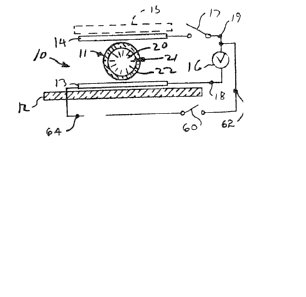
Turning now to Fig. 2, an improved liquid crystal
device in accordance with the present invention is
indicated at 10. The device 10 includes an encapsu-
lated liquid crystal 11 having a smectic phase which
is supported by a mounting substrate 12 across which
an electric field may be applied via electrodes 13,
1~ .
The electrode of 13 may be, for example, a quantity of
vacuum deposited indium tin oxide applied to the
substrate 12, and the electrode 14 may be, for
example, electrically conductive ink. A pxotective
layer or coating 15 may be applied over the electrode
14 for protective purposes but such layer 15 ordi-
narily would not be necessary for supporting or
confining the encapsulated liquid crystal 11 or the
electrode 14. Voltage may be applied to the elec-
trodes 13, 14 from an AC or DC voltage source 16. A
selectively closable switch 17 and electrical leads
~2~?`3 1~7
-17-
18, 19 are utilized to apply an electric field across
the encapsulated liquid crystal 11 when the switch 17
is closed. A second selectively closable switch 60 and
electrical leads 62, 64 may be utilized to provide a
resistive heating source for the application of heat
to the liquid crystal material to increase the temper-
ature thereof for the purposes hereinafter described.
Switch 60 may be closed to cause a suitable current to
flow through electrode 13 so as to heat the liquid
crystal material to the desired level. Other tech-
niques, such as a heat gun, may be utilized to heat
the liquid crystal material.
The encapsulated liquid crystal 11 includes liquid
crystal material 20 contained within the confines or
interior volume 21 of a capsule 22. Preferrably, the
capsule 22 is generally spherical. However, the
principles of the invention would apply when the
capsule 22 is of a shape other than spherical. Such
shape should provide the desired optical and elec-
trical characteristics that will satisfactorily
coexist with the optical characteristics of the liquid
crystal 20, e.g., index of refraction, and will permit
an adequate portion of the electric field to occur
across the liquid crystal material 20 itself for
effectlng desired alignment of the liquid crystal
structure when it is desired to have a field on
condition. A particular advantage to the preferred
spherlcal configuration of the capsule 22 will be
described below with respect to the distortion it
effects on the llquid crystal structure.
The mounting substrate 12 and the electrodes 13, 1~ as
well as the protective coating 15 may be optically
transmissive so that the liquid crystal device 10 ls
capable of controlling transmisslon of light there-
~2~@} 3~
-18-
through in response to whether or not an electric
field is applied across the electrodes 13, 14 and,
thus, across the encapsulated liquid crystal 11.
Alternatively, the mounting substrate 12 may be
optically reflective or may have thereon an optically
reflective coating so that reflection by such reflec-
tive coating of incident light received through the
protective coating 15 will be a function of whether or
not there is an electric field app:Lied across the
encapsulated liquid crystal 11.
Preferably, a plurality of encapsulated liquid crys-
tals ll would be applied to the mounting substrate 12
in a manner such that the encapsulated liquid crystals
adhere to the mounting substrate 12 or to an interface
material, such as the electrode 13, for support by the
moun-ting substrate 12 and xetention in a fixed posi-
tion relative to the other encapsulated liquid crys-
tals 11. Most preferably the encapsulating medium of
which the capsule 22 is formed is also suitable for
binding or otherwise adhering the capsule 22 to the
substrate 12. Alternatively, a further binding medium
(not shown) may be used to adhere the encapsulated
liquid crystals 11 to the substrate 12. Since the
capsules 22 are adhered to the substrate 12, and since
each capsule 22 provides the needed confinement for
the liquid crystal material 20, a second mounting
substrate, such as the additional one shown in the
prior art liquid crystal device 1 of Fig. 1, ordi-
narily would be unnecessary. However, for the purpose
of providing protection from scarring, electrochemical
deterioration, e.g., oxidation, or the like, of the
electrode 14, a protective coating 15 may be provided
on the side or surface of the liquid crystal device 10
opposite the mounting substrate 12, the latter provid-
ing the desired physical protection on its own side of
the device 10.
~ ':
9~7~
--19--
Since the encapsulated liquid crystals 11 are rela-
tively securely adhered to the substrate 12 and since
there ordinarily would be no need for an additional
substrate, as mentioned above, the electrode 14 may be
applied directly to the encapsulated liquid crystals
21.
Turning now to Fig. 3, an example of a liquid crystal
device 10' in accordance with the invention is shown
in the form of a liquid crystal display device, which
appears as a square cornered figure eight 30 on the
substrate 12, which in this case preferably is of a
plastic material, such as Mylar, or may alternatively
be another materi.al, such as glass, for example. The
shaded area appearing in Fig. 3 to form the square
cornered figure eight is formed of plural encapsulated
liquid crystals 11 arranged in one or more layers on
and adhered to the substrate 12.
An enlarged fragmentary section view of a portion 32
of the figure eight 30 and substrate 12 is illustrated
in Fig. 4. As is seen in Fig. 4, on the surface 31 of
the substrate 12, which may be approximately 10 mils
thick; is deposited a 200 angstrom thick electrode
layer 33 of, for example, indium tin oxide or other
suitable electrode material such as gold, aluminum,
tin oxide, antimony tin oxide, etc. One or more
layers 34 of plural encapsulated liquid crystals 11
are applied and adhered directly to the electrode
layer 33O Such adherence is preferably effected by
the encapsulating medium :that forms respective cap-
sules 22, although, if desired, as was mentioned
above, an additional adhering or binding material may
be used for such adherence purposes. The thickness of
the layer 34 may be, for example, approximately 0.3 to
10 mils, preferably 0.7 to 4 mils, more preferably 0 8
~ l~rade ll/l~r~
3~L7
-20-
to 1.2 mils, especially 1 mil. Other thicknesses may
also be used, depending inter alia on the ability to
form a thin film and the electrical breakdown proper-
ties of the film. A further electrode layer 35 is
deposited on the layer 34 either directly to the
material of which the capsules 22 are formed or,
alternatively, to the additional binding mate~ial used
to bind the individual encapsulated liquid crystals 11
to each other and to the mounting substrate 12. The
electrode layer 35 may be, for example, approximately
~ mil thick and may be formed, for example, of elec-
trically conductive ink or of the materials mentioned
above for layer 33. A protective coating layer 36 for
the purposes described above with respect to the
coating 15 in Fig. 3 also may be provided as is shown
in Fig. 4.
In a conventional visual display device either of the
liquid crystal or light emitting diode type, the
figure eight element 30 ordinarily would be divided
into seven electrically isolated segments~ each of
which may be selectively energized or not so as to
create various numeral characters. For example,
energization of the segments 3~a and 30b would display
the numeral "1", and energization of the segments 3Oa,
30b, and 30c would display the numeral "7".
A feature of the present invention utilizing the
encapsulated liquid crystals 11 is that a versatile
substrate 12 can be created to be capable of display-
ing virtually any desired display as a function of
only the selective segments of conductive ink elec-
trodes printed on the liquid crystal material. In
this case, the entire surface 31 of the substrate 12
may be coated with electrode material 33, and even the
entire surface of that electrode material may be
.
., ~ .
-21-
coated substantially contiguously with layer 34 of
encapsulated liquid crystals 11. Thereafter, a
prescribed pattern of electrode segments of conductive
ink 35 may be printed where desired on the layer 34.
A single electrical lead may attach the surface 31 to
a voltage source, and respective electrical leads may
couple the respective conductive ink segments via
respective controlled switches to such voltage source.
Alternatively, the encapsulated liquid crystals 11
and/or the electrode material 33 may be applied to the
surface 31 only at those areas where display segments
are desired. The ability to apply encapsulated liquid
crystal to only a desired area or plurality of areas
such as the segments of a display by essentially
conventional processes (such as e.g. silk-screening or
other printing processes) is particularly attractive,
when compared with the prior art, which has the
probl~m of containing liquid crystals between flat
plates.
Although a detailed description of the operation of
the individual encapsulated liquid crystals 11 will be
presented below, it will suffice here to note that the
encapsulated liquid crystals in the layer 3~ function
to attenuate or not to attenuate light incident
thereon. A pleochroic dye may be present in solution
in the liquid crystal material to provide substantial
attenuation by absorption prior to the application of
the ~ield but to be substantially transparent after
the field has been applied. Such an electric field
may be, for example, one produced as a result of the
coupling of the electrode layer portions 33, 35 at an
individual segment, such as segment 30a, of the liquid
crystal device 10' to an electrical voltage source.
The magnitude o~ the electric field required to switch
the encapsulated liquid cr~stals 11 from a no field
.. .... .
~2~3~
-22-
(deenergized) condition to a field-on (energized)
condition may be a function of several parameters,
including, for example, the diameter of the individual
capsules and the thickness of the layer 34, which in
turn may depend on the diameter of individual capsules
22 and the number of such capsules in the thickness
directio~ of layer 34. Importantly, it will be
appreciated that since the liquid crystal material 20
is confined in respective capsules 22 and since the
individual encapsulated liquid crystals 11 are secured
to the substrate 12, the size of the liquid crystal
device 10' or any other liquid crystal device employ-
ing encapsulated liquid crystals in accordance with
the present invention is virtually unlimited. Of
course, at those areas where it is intended to effect
a change in the optical properties of the encapsulated
liquid crystals of such a device in response to a no
field or field on condition, it would be necessary to
have at such areas electrodes or other means for
applying to such liquid crystals a suitable electric
field.
The electrode layer 33 may be applied to the substrate
12 by evaporation, by vacuum deposition, by sputter-
ing, by printing or by another conventional technique.
Moreover, the layer 34 of encapsulated liquid crystals
11 may be applied, for example, by a web or gravure
roller or by reverse roller printing techniques. The
electrode layer 35 also may be applied by various
printing, stenciling or other techniques. If desired,
the electrode layer 33 may be prepared as a full
coating of the substrate 12, such as Mylar, as de-
scribed above, as part of the process in which the
Mylar sheet material is manufactured, and the layer 34
also may be applied as part of such manufacturing
process.
~L2~e~3~
-23-
Electrode 33 may be attached to a voltage source
through a selectively closable switch 60 separate from
the respective controlled switches utilized to ener-
gi~e the conductlve segments. When switch 60 is
pulsed closed, electrode 33 functions as a resistive
heating element that applies heat to the liquid
crystal material to increase the temperature thereof.
If the liquid crystal material has both a smectic and
nematic phase, heat may be applied, by closing switch
60, to heat the liquid crystal through its transition
temperature where it changes from the smectic to the
nematic phase. Thereafter, an electric field (across
electrodes 33, 35) can be applied to the liquid
crystal material, now in the nematic phase, such that
the liquid crystal material is substantially transpar-
ent to effect a visual display, such as the numeral
"1". (See Fig. 6). The temperature of the liquid
crystal may then be reduced, by opening switch 60, so
that the liquid crystal is in the smectic phase. The
electric field may then be removed. The display,
however, will be retained (See Fig. 8a), e.g., the
numeral "1", since the molecules of the liquid crystal
in the smectic phase are not free to change direction
and the liquid crystal is more viscous in this phase.
The above-described concept may be called a thermally-
activated dlsplay.
To erase the display, switch 60 may again be pulsed
closed to heat the liquid crystal above its transition
temperature where it is in the nematic phase. As
discussed, in the nematic phase, incident light is
absorbed or scattered in the absence of an electric
field ~See Fig. 8b). Thus, the display is effectively
erased. The display may also be erased by heating the
:~: .' ,,
,. ;
: . '; . ~
~7~31 ~
-24-
liquid crystal so that it is in its isotropic phase
wherein incident light is scattered or absorbed.
A liquid crystal material having only a smectic phase
may also be utilized in the concept of the present
invention. The smectic phase may either be smectic A
phase or smectic C phase. The smectic C phase oper-
ates at lower voltages than smectic A, and the smectic
C phase may have a chiral character. An electric
field may be applied across the liquid crystal ir. the
smectic phase to eliminate the scattering or absorp-
tion of light otherwise present ~See Fig. 6). The
display formed by the application of the electric
field, such as the numeral "1", remains after the
field is removed (See Fig. 8a). The display may be
thereafter erased by heating the liquid crystal to a
temperature above the smectic to isotropic phase
transition temperature. Alternatively, it may be
erased by heating it to a temperature above the
smectic to nematic phase transition temperature. This
display concept may be called the heat-to-erase
concept. It differs from the thermally-activated
display in that the field is applied and display
effected with the li~uid crystal in the smectic phase.
The smectic phase encapsulated system which operates
at moderate voltages can be used to form a novel type
of display. The principle is based on the
above-described ability of smectic liquid crystal to
store indefinitely when exposed to an electric field.
Thus a display can be made using a matrix of elements,
such that there is a cross-grid formed. A permanent
pattern can be formed on the cross-grid by elevating
voltage on the lines and rows to be written, simul-
taneously. Thus, rows not written can be put at a
~7~3~
-25-
voltage which is close to that of the columns. The
same voltage, with opposite polarity, can be put on
those rows to be written, so that a voltage appears
across the column/row intersection which is two times
greater than that applied to rows which are not to be
written.
If this process is carried out in sequence at a rate
sufficiently slow so that RMS increases in voltage do
not occur across row/column intersections, then a
pattern can be formed which will remain in place until
such time as the display is heated Ito erase) to the
phase transition of the smectic liquid crystal.
The heat-to-erase and the thermally-activated displays
are especially suitable for use in display devices
where there is relatively long time periods between
changes in or updates of the display. The displays
may also be used as a temperature indicating label to
indicate when there is a temperature rise above a
certain level. For example, certain chemicals must be
stored below a given temperature. A label reading
"OK," e.g., may be applied to a container holding the
chemicals. The "OK" display would disappear or be
erased when the temperature rises above the undesir-
able or even dangerous level.
The ability to make and to use successfully heat-to-
erase and thermally activated liquid crystal devices
of the type just described is in part due to the
ability to make encapsulated liquid crystals and to
the properties of such encapsulated liquid crystals,
both of which are features of the present invention.
These features now will be described.
... . :
; . ~ ::
. . ,, ,., .. :... ..
' ' '" ' "' " '" ' '.' "
,;
~L2~3~L7
Referring specifically to Fig. 5, the capsule 22 has a
generally smooth curved interior wall surface 50
defining the boundary of the volume 21. The actual
dimenslonal parameters of the wall surface S0 and of
the overall capsule 22 are related to the qua~tity of
liquid crystal material 20 contained therein. Addi-
tionally, the capsule 22 applies a force to the liquid
crystals 20 tending to pressurize or at least to
maintain substantially constant the pressure within
the volume 21. As a result of the foregoing, and due
to the surface wetting nature of the liquid crystal,
the struckure which ordinarily in free form would tend
to be straight, although perhaps randomly distributed,
is distorted to have a generally focal conic form. Due
to such distortion the liquid crystals store elastic
energy. For simplicity of illustration, and for
facility of comprehending the foregoing concept, the
liquid crystal molecules whose directional orientation
is represented by respective dashed lines 52 is shown
as having a bulk alignment wherein the liquid crystal
molecules radiate from a central portion of the
capsule to be generally perpendicular to a relatively
proximate portion of the interior wall surface 50.
Thus, the organization of liquid crystal molecules in
an individual capsule is determined by the bulk
alignment of the molecules within the capsules unless
acted on by outside forces, e.g., an electric field.
As noted heretofore, on removal of the field, the
directional orientation illustrated in Fig. 6 of the
smectic liquid crystal remains (See Fig. 8a). The
distorted alignment depicted in Fig. 5 returns upon
the application of heat to the liquid crystal to heat
it above the phase transition temperature (See Fig.
8b).
~Z~3~
-27-
The liquid crystal molecules have a smectic phase.
Such molecules usually assume a parallel configura-
tion, and a liquid crystal material comprised of such
molecules usually is optical polarization direction
sensitive. However, since the structure 52 in the
encapsulated liquid crystal 11 is distorted or forced
to assume focal conic form shown in Yigs. 5 or 8b in
the full three dimensions of the capsule 22, such
liquid crystal material in such capsule takes on an
improved characteristic of being insensitive to the
direction of optical polarization of light incident
thereon. Moreover, when the liquid crystal material
in the capsule 22 has pleochroic dye dissolved
therein, such dye, which ordinarily also would be
expected to have optical polarization sensitivity, no
longer is polarization sensitive because the dye tends
to follow the same kind of orientation or distortion
as that of the liquid crystal structure.
With ~he liquid crystal structure being distorted
generally in the manner illustrated in Figs. 5 and 8b,
the encapsulated liquid crystal 11 ordinarily will
absorb or block light from being transmitted there-
through prior to the application of an electric field
across the encapsulated liquid crystal 11 and particu-
larly across the liquid crystal material 20 thereof.
Although the foregoing discussion has been in terms of
a homogeneous orientation of the liquid crystal
material, such is not a requisite of the invention.
All that is required is that the interaction between
the capsule and the liquid crystal produce an orient-
ation in the liquid crystal that is generally uniform
and piecewise continuous, so that the spatial average
orientation of the liquid crystal material over the
capsule volume is generally focal conic and there is
: ~.
, ', .' ' ,
: ` : :
.,. ~ ,..
-:
7~ 7
-28-
no substantial parallel directional orientation of the
llquid crystal in the absence of an electric field.
It is this orientation that results in the
absorption/scattering and polarization insensitivity.
However, when an electric field is applied across the
encapsulated liquid crystal 11 in the manner illus-
trated in Fig. 6, the liquid crystal and any
pleochroic dye in solution therewith will align in
response to the electric field in the manner shown in
such figures. 5uch alignment permits light to be
transmitted through the encapsulated liquid crystal
11, for example as described above with reference to
Figs. 2, 3 and 4.
When the electric field is removed, the alignment of
the liquid crystal as shown in Fig. 6 remains. The
application of heat to the liquid crystal as shown in
Fig. 8b causes the liquid crystal to return to the
distorted alignment illustrated in Fig. 5.
To optimize the contrast characteristics of a liquid
crystal device, such as that shown at 10' in Fig. 3,
comprised of encapsulated liquid crystals 11, and more
particularly, to avoid optical distortion, due to
refraction of incident light passing from the encapsu-
lating medium into the liquid crystal material and
vice versa, of the encapsulated liquid crystal 11 of
Fig. 6, the index of refraction of the encapsulating
medium and that the ordinary index of refraction of
the liquid crystal material should he matched so as to
be as much as possible the same. The closeness of the
index matching will be dependent on the desired degree
of contrast and transparency in the device, but the
ordinary index of refraction of the crystal and the
:,,,
''~,.' :' '
.. .. .
,
~'; ~ ':"''' ' . .
. : . : .
~7~
-29- 1051-1974
index of the medium ~ill preferably dif-er by no more
than 0.03, more preferably 0.0l, especially 0.001.
The tolerated difference will depend on capsule si~e
and intended use of the device. The tex~ "Optics" by
Sears, published by Addison-Wesley, contains a thor-
ough discussion of birefringence relevant to the
foregoing.
However, when no field is applied there will be a
differenee in indices of refraction at the boundary of
the liquid crystal and capsule wall due to the extra-
ordinary index of refraction of the liquid cr~stal
being greater than the encapsulating medium. This
causes refraction at that lnterface or boundary and
thus further scattering and is a reason why encapsu-
lated liquid crystal material in accordance with the
present invention, in partieular, will function to
prevent transmission of light even without the use of
pleochroic dye.
Orcinarily the eneapsulated liquid crystals 11 wGuld
be applied to the substrate 12 (Fig. 3) such that the
individual encapsulated liquid erystals 11 are rela-
tively randomly oriented and preferably several
capsules thiek to assure an adequate quantity of
liquld erystaI material on the surfaee 31 of the
su~strate to thereby provide the desirec level o
light blockage and/or transmission eharacterist-cs
for, for example, a liauid crystal device lQ' or t~le
like.
In a liquid crystal device, such as that shown in lQ'
in Fig. 3, which is comprised of liquid crystal
material 20 including pleochrcic dye to form enca?su-
lated liquid cr~stals 11 according to the in~ention,
' " :. ' ,
,.; :
7~3~
-30-
it has ~een discovered that the degree of optical
absorbency is at least about the same as that of
relatively free (unencapsulated) liquid crystal
material, including pleochroic dye such as that shown
in Fig. 1. It also has been discovered unexpectedly
that when the electric field is applied in the manner
illustratea in Fig. 6, for example, the clarity or
lack of opaqueness of the encapsulated liquid crystal
material 20 including pleochroic dye is at least about
the same as that of the ordinary case in the prior art
device 1 having dye in solution with relatively free
liquid crystal material.
:
It is important that electrical field E shown in Fig.
6 is applied to the liquid crystal material 20 in the
capsule 22 for the most part rather than being dissi~
pated or dropped substantially in the encapsulating
material of which the capsule itself is formed. In
other words, it is important that there not be a
substantial voltage drop across or through the mate-
rial of which the wall 54 of the capsule 22 is formed;
rather, the voltage drop should occur predominantly
across the liquid crystal material 20 within the
volume 21 of the capsule 22.
~`
The electrical impedance of the encapsulating medium
preferably should in effect be sufficiently larger
than that of the liquid crystal material in the
encapsulated liquid crystal 11 so that a short circuit
will not occur exclusively through the wall 54, say
from point A via only the wall to point B, bypassing
the liquid crystal material. Therefore, for example,
the effective impedance to induced or displacement
current flow through or via the wall 54 from point A
only via the wall 54 to point B should be greater than
the impedance that would be encountered in a path from
,,,.... ~
: , : . ,
~.:, .. :.
.
'' ' :
-31-
point A to point A' inside the interior wall surface
50, through the liquid crystal material 20 to point B'
still within khe volume 21, thence ultimately to point
B again. This condition will ensure that there will
be a potential difference between point A and point s,
which should be large enough to produce an electric
field across the liquid crystal material that will
tend to align it. It will be appreciated that due to
geometrical considerations, namely the length through
only the wall from point ~ to point B, for example,
that such a condition can still be met even though the
actual impedance of the wall material may be lower
than that of the liquid crystal material contained
therein.
~,
The dielectric constants (coefficients) of the mate-
rial of which the encapsulating medium is formed and
of which the liquid crystal material is comprised and
the effective capacitance values of the capsule wall
54, particularly in a radial direction, and of the
liquid crystal material across which the electric
:
~ field E is imposed should all be so related that the
,
wall 54 of the capsule 22 does not substantially
decrease the magnitude of the applied electric field
E.
A schematic electric circuit diagram representing the
circuit across which the electric field E of Fig. 6 is
imposed is illustrated in Fig. 7. The electric field
is derived from the ~oltage source 16 when the switch
17 is closed. A capacitor 70 represents the capaci-
tance of the liquid crystal material 20 in the encap-
sulated liquid crystal 11 when such electric field is
applied in the manner illustrated in Fig. 6. ~he
capacitor 71 represents the capacitance of the wall 54
of the capsule 22 at an upper area tthe direc~ion
.
: , :
....
~27~3~
-32- 61051-1974
conveniently referring to the drawing but having no
other particular meaning) and is, accordingly~ curved
in a manner similar to that o the upper portion of
the capsule 22 of Figs. 5 and 6. The capacitor 72
similarly represen~s the capacitance of the lower
portion of the capsule exposea to the electric field
E. The magnitudes of capacitance for each capacitor
7Q-72 will be a function of the dielectric constant
(coefficient) of the material of which *he respective
capacitors are formed and of the spacing of the
effective plates thereof. It is desirable that the
voltage drop occurring across the respective capaci-
tors 71, 72 will be less than the voltage drop across
the capacitor 70; the result, then, is application of
a maximum portion of the electric,field E across the
liquid crystal material 20 in the encapsulated liquid
crystal 11 for achieving optimized operation, i.e.,
alignment, of the liquid crystal molecules thereof
with a minimum total ehergy requirement of the voltage
source 16. However, it is possible that the voltage
drop in one or both capacitors 71, 72 will exceed the
voltage drop across capacitor 70; this is operation-
ally acceptable as long as the drop across the capaci-
tor 70 (liquid crystal material) is great enough to
produce an electric field that tends to align the
liquid crystal material to and/or toward-the field-on
condition of Fig. 6, for example.
In connection with capacitor 71, for example, the
dielectric material is that of which ~he wall 54 is
formed relatively neax the upper portion of the
capsule 22. The effective plates of such capacitor 71
are the exterior and interior wall surfaces 73, 50,
and the same is true for the capacitor 72 at the lower
;: portion of the capsule 22 relative ~o the illustration
of Fi~. 6, for example. ~y making ~the wall 54 as thin
`~`'h
~7~3:1~7
-33-
as possible, while still providing adequate strength
for containment of the liguid crystal material 20 in
the volume 21, the magnitudes of capacitors 71, 72 can
be maxlmized, especially in comparison to the rather
thick or lengthy distance between the upper portion 74
of the liquid crystal material 2~ of the lower portion
75 th~xeof which approximately or equivalently form
the plates of the same number of the capacitors 70.
The liquid crystal material 20 will have a dielectric
constant value that is anisotropic. It is preferable
that the dielectric constant (coefficient~ of the wall
54 be no lower than the lower dielectric constant
(coefficient) of the anisotropic liquid crystal
material 20 to help meet the above conditions. Since
a typical lower dielectric constant for liquid crystal
material is about 6. This indicates that the dielec-
tric constant of the encapsulating material is prefer-
ably at least about 6. Such value can vary widely
depending on the liquid crystal material used, being,
for example, as low as about 3.5 and as high as about
8 in the commonly used liquid crystals.
The encapsulated liquid crystal 11 has features such
that since the liquid crystal structure is distorted
and since the pleochroic dye similarly is distorted,
absorbency or blockage of light transmission through
the encapsulated liquid crystals will be highly
effectiveO On the other hand, due both to the effi-
clent application of an electric field across the
liquid crystal material 2~ in the encapsulated liguid
crystal 11 to align the liquid crystal molecules and
the dye along therewith as well as the above described
preferred index of refraction matching, i.e., of the
encapsulating medium and of the liguid crystal mate-
rial, so that incident light will not be refracted or
:: .. ~:. - :
-. ,: .
~:
~:7~33L7
-3~- 61051-1974
bent at ~he interface between ~he capsule wall 54 and the liquid
crystal material 20 when an electric ~ield is applied, the
encapsulated liquid crystal 11 will have a yood op~lcally
transmlssive characteris~ic.
Since a plurality of encapsulated llguid cry ~als 11
ordinarily is required to cons~ruct a final li~uid crystal device,
such as the devlce 10' of Figure 3, and since those encapsulated
liquid crystals are ordinarily present in several layers, it is
desirable for the liquid crystal material to have a relatively
high die~ectric anisotropy in order to reduce the voltage
requirements for the electric field E. More specifically, the
differential between the dielectric constant (coefficient) for the
liquid crystal material ~0 when no electric field is applied which
constant (coefficient) should be rather ~mall, and the dielectric
constant (coefficient) for the liquid crystal material when an
electric fleld is applied, which constant ~coefficient~ should be
rela~ively large, should be as large as possible consistent with
the dielectric of the encapsulating medlum.
The capsules 22 may be of various sizes. Also, when the
capsule size is relatively smallr more capsules are re~uired per
unit area of the layer 34, and, therefore, more electric voltage
drop losses will occur in the encapsulating medium than for larger
size capsules, the density per unit area of which would be
; smaller. Preferahly, a device made with the encapsulated liquidcrystals 11, such as the liquid crystal device 10', should use
capsules of unlform size so ~hat the device 10' can be energized
or deenergized in a relatlvely uni~orm and well con~rolled manner.
h; , ~
, ~ .
~27~ 7
-35~ 61051~1974
In constrast, when the capsules are of a non~uniform size, the
non~uniform eneryization of the respec~ive capsules, i.e.,
alignment of the liquid cry~tal molecules of each, would occur
upon application of the elec~ric ~ield. Ordinarily the capsules
22 should have a size on the order o~ from about 1 to ahout 30
microns in dia~e~er.
Currently a sui~able liquid crystal material i5 smectic.
A phase material S2 sold by BDH Chemical, Pool, England. Another
suitable liquid cry~tal materlal may be formed by mixin~, in the
proportions indicated in parenthesis, the following liquid
crystals supplied by ~. Merck Chemicals, Darmstadt, West Germany:
K24 (18.7%), K30 ~27%), R36 (40.8~), ZLI 1840 (6.5%), and C~15
(7~).
The encapsulating medium forming capsules 22 shoulcl be
of a type that is ~ubstantially completely unaffected by and does
no~ react with or otherwise chemically affect the liquid crystal
materlal. In particular, ~he liquid crys~al material should not
be soluble in the encapsulating medium or v$ce versa. The other
characteristics descrlbed above concerning dielectric constants
(coefficients) and indices or refraction with respect to the
liquid crystal material and to the
",`
-36-
encapsulating medium also constrain material selec-
tion. Moreover, when a pleochroic dye is employed,
the encapsulating medium also should be unaffected by
and should not affect the dye material. On the other
hand, the dye should be soluble in the liquid crystal
material and not subject to absorptlon by the encapsu-
lating medium. Additionally, to achieve the desired
relatively high impedance for the encapsulating
medium, such medium should have a relatively high
level of purity. Especially when the encapsulating
medium is prepared as an aqueous dispersion or by
ionic polymerization, etc., it is important that the
level of ionic (conductive) impurities should be as
low as possible.
Examples of pleochroic dyes that may suitably be used
in the encapsulated liquid crystals 11 in accordance
' `7''"`' with the present invention are indophenol blue, Sudan~
black B, Sudan~ 3, and Sudan 2, and D-37, D-43 and D-85
by E. Merck identified above.
Polyvinyl alcohol (PVA) r which has been found to have
the desired properties mentioned above, may be
utilized as an encapsulating medium when the encap-
sulation is performed by emulsification. PVA has a
good, relatively high, dielectric constant and has an
index of refraction that is relatively closely matched
to that of the preferred liquid crystal material.
To purify PVA, the same may be dissolved in water and
washed out with alcohol using a precipitation tech-
nique. Other techniques also may be used for puri-
fying PVA so that it will have minimum salt or other
content that would reduce appreciably the electrical
impedance thereof. A preferred purified PVA is
Gelvatol sold by M~nsanto. If PVA is properly
:~
~ ~r~ d e
,
~27~3~L~7
-37-
puri~ied, as aforesaid, it will serve well as its own
emulsifier and as a wetting agent for facilitating the
manufacture of encapsulated liquid crystals according
to this method which will be descr:ibed ~elow. Other
types of encapsulating medium may be, for example,
gelatin; Carbopole, (a carboxy polymethylene polymer
of B.F. Goodrich Chemical Corporation) Gantrez;
Ipolymethyl vinyl ether/maleic anhydride) of GAF
Corporation, preferably reached with water to form the
acid, the latter two being polyeleetrolytes. ~hese
media may be used alone or in combination with other
polymers, such as PVA.
Other examples and characteristics of se~eral PVA
materials are shown in Table I.
An emulsion method for making encapsulated liquid
crystals 11 may include mixing together the encapsu-
lating medium, the liquid crystal material (including,
if used, the pleoehroic dye material), and perhaps a
carrier medium, sueh as water. Mixing may occur in a
variety of mixer devices, such as a blender, a eolloid
mill, whieh is most preferred, or the like. What
occurs during such mixing is the formation of an
emulsion of the ingredients, which subsequently ean be
dried eliminating the carrier medium, such as water
and satisfactorily euring the eneapsulating medium,
such as the PVA. Although the capsule 22 of each
thusly made eneapsulated liquid erystal 11 may not be
a perfect sphere, eaeh capsule will be substantially
spherieal in configuration because a sphere is the
lowest free energy state of the individual droplets,
globules or capsules of the emulsion, both when
originally formed and after drying and/or euring has
occurred.
~ de /~
~p
,~
7~3~
10 ~ ' 11 t 9
: ~ W ~ ~ j I I
3 ~ a 9
3 ~ o
O ~ 3 j 9
~S W 011 0
k 1~ ' D
G I W ~ ~ ~ ~ 0
; ~ o ~ R
1 C c o
,~-U j~-
~.
~ .... .. `
~2~3~7
-3~ 61051-1974
Another encapsulating medium is la~ex. Latex may be a
suspenælon of na~uxal rubber or synthetic polymer or copolymer
particles. A la~ex medium i6 formed by drying a suspension of
such particles.
- ~riefly, latex entrapped liquid crystal may be formed by
mixing a suspension of latex particles and liquid crystal material
wherein the liguid crys~al material has been previously emulsified
in an aqueous phase. Alternatively, all components may ba
combined prior to emulsifying the liquid crystal material. The
mixture may then be applied to a substrate. As the mixture dries,
it adheres to the substrate. When drled, the latex particles form
a latex medium wikh particles of liquld crystal dispersed therein.
It is noted here ~hat the characteristic of the
pleochroic dye that it must be solubla in the li~uid crystal
material and that it not be subject to absorption by the water
phase or polymer phase assures that such pleochroic dye will no~
2Q be absorbed by the PVA, latex or other encapsulating medium or by
the carrier mediumr such as the water, used during the
manufacturing process for the encapsulated liquid crystals 11.
'
:`
~"
~27~
-39-
EXAMPLE l
A liquid crystal material having a smectic phase was
formed by mixing the following liquid crystal mate~
rials, available from E. Merck Chemicals, Darmstadt,
W. Germany:
K24 18.7%
~30 27.0
K36 40.8%
ZLI 1840 6.5~
CB 15 7.0%
In order to insure good mixing, the components were
dissolved in chloroform. The resulting temperature
range was:
0C to 46C - smectic A
46C to 48C - cholesteric
:
The smectic liquid crystal (SLC) mixture was emulsi-
fied in a polymer solution which contained 92.5~ PVA
~;~ 20/30 (available from Airco, Allentown, Pennsylvania)
in an 80% water solution, 5% Gantrez 169 (89~ water
solution) and 2.5% glycerol.
~:`
The ratio of SLC mixture to PVA matrix was 1:2. The
resulting emulsion was coated onto a Mylar film which
had been previously evaporated with indium tin oxide
~ITO). Use of a 2 mil-spaced doctor blade resulted in
a dry film thickness of .5 mils.
The film was laminated to a second piece of ITO-coated
` ~ylar, then placed in an oven at 100C for one hour.
The result was a liquid crystal cell which was activ-
ated at lOOVDC, i.e~, it became transparent. When the
field was removed, the film remained transparent.
-40-
Lesser voltages resulted in somewhat fewer degrees of
alignment. In all cases, the liquid crystal emulsion
remained in a state of activation. When the film was
heated to 46C or above (heat-to-erase), its transi-
tion temperature, it returned to its original state,
i.e., scattering.
:
~,
EXAMPLE 2
Materials and procedure same as in Example 1, and
further, M141, a 3~ blue dye (available from Mitsui
Toatsu Chemicals, Tokyo, Japan) was added to the above
mixture, using chlorofoxm as a solvent.
When the electric field was applied to the cell, the
color changed from dark opaque blue to light trans-
parent blue.
` :
~ EXAMPLE 3
r~
" 1,
Same as Example 2, but a 3% yellow dye (G232 from
Mitsui Toatsu Chemicals) was added. As a result, the
:
~; cell changed from a dark opaque orange to a light
transparent yellow when the electric field was ap-
~ plied.
: :
`'~
EXAMPLE 4
A liquid crystal mixture was made which contained
three parts K24 and one part CE3, both liquid crystals
available from E. Merck. The resulting material was a
smectic C at room temperature ~24C), but became
'
' '''
:~ .
`'. , '`
~L27~13~L~
-41- 61051-1974
smectic A at 58~. The smectic A became cholesteric at
68.1. At 76.6 the material became isotropic.
When an electric field of 60V was applied to the
resulting cell, it ~ecame transparent and the ~rans-
parency remained un~il it was heatecl to about 76.6 .
In accordance with the present invlention the quanti-
ties of ingredients for making the encapsulated liquid
crystals 1l, for example in the manner described
above, may be, as follows:
The liquid crystal material - This material may be
from about 5~ to about 20% and preferably about 50~
(and in some circumstances even greater depending on
the nature of the encapsulating material) including
the pleochroic dye of the total solution delivered to
the mixing apparat~s, such as a colloid mill. The
actual amount of liquid crystal material used should
ordinarily exceed the volume quantity of encapsulating
medium, e.g., PVA to optimize the capsule size.
The PVA The quantity of PVA in the solution should
be on the order of from a~out 5% to about 50~, and
possibly even greater depending on the hydrolysis and
molecular weight of the PVA, and preferably, as
described above, about 22~. For example, if the PVA
has too large a molecular weight, the resulting mate-
rial will ~e like glass, especially if too much P~A is
used in the solution. On the other hand, if the
molecular weight is too low, use of too little PVA
will result in too low a viscosity of the material,
and the resulting emulsion solidify adequa~ely to the
desired spherical encapsulated liquid crystals.
A ~ ~
,"' ~'~ ` ' '
~ ',
~7~
-42-
Carrier medium - The remainder of the solution would
be water or other, preferably volatile, carrier
medium, as described abo~e, with which the emulsion
can be made and the material laid down appropriately
on a substrate, electrode or the like.
EXAMPLE 5
A method of making latex entrapped smectic liquid
crystal may comprise adding .03 grams of the surfac-
tant Igepol C0720 ~available through GAF, N.Y., NY)
and .03 grams of the surfactant DOW 5098 (available
through Dow Chemical, Midland, Michigan) to 2.09 grams
of S2 smectic liquid crystal material (available
through BDH Chemicall Pool, England), and thereafter
heating the composition to its isotropic temperature
to dissolve ito The mixture may then be cooled to
room temperature (24C) and .5 grams of MeC12 added to
dissolve it. Then, 3.0 grams of Neorez R-967 (avail-
able through Polyvinyl Chemicals, Wilmington, ~ass.)
containing 40% of latex particles by weight may be
added and mixed with an impeller blade at 2400 RPM for
3 minutes. Thereafter, .2 gra~ms of a 5~ solution of
the cross-linking agent Tyzor LA (available through
DuPont, Wilmington, Del.) is added with slow mixing at
about 300 RPM.
The resulting temperature range was:
0C to 48C - smectic A
48C to 49C - nematic
above 49C - isotropic
With no field, incident light was scattered. The
liquid crystal was in the nematic phase when heated to
~ 1'r~ r~
:
,
,
~ ~ ,
`` ~27~3~7
-43- 61051- 1974
about 4BC, its transition temperature. An applied
electric field permitted light ~D be transmitted
through the liquid crystal. The liquid crystal cooled
~o room temperature and the field~was removed. Light
was still transmitted through the liquid crystal. To
cause scattering, the liquid crystal was again heated
to its transition temperature of about 4~C.
EXAMPLE 6
Same as Example 5 but a l~ Bl blue dye (availahle
through ~. Merck) was added to the 32 liquid crystal
material. As a result, when an electric field was
applied, the color changed from opaque blue to light
transparent blue.
It will be appreciated ~hat since the uncured capsules
or droplets of encapsulating medium and liquid crystal
material are caxried in a liquid, various conventional
or other techniques may be employed to grade the
capsules according to size so that the capsules can be
reformed if of an undesirable size by feeding again
through the mixing apparatus, for example, and so that
the finally used capsules will be of a desired uni-
formity for the reasons expressed above.
Although an encapsulation technique has been described
with reference to emulsification, since ~he fact that
the encapsulant material and binder are the same makes
facile the production of liquid crystal devices; the
preparation of discre~e caps~les of the liquid crystal
material may on occasion be advantageous, and the use
of such discrete capsules (with a binder) is within
the contemplated scope of this invention.
I
~7~3~L~
-44-
Although certain specific embodiments of the invention
have been described herein in detail, the invention is
not to be limited only to such embodiments, but rather
only by the appended claims.
~.~
:,;
,,
~;
;~``
~,-
" '' : ' -