Note: Descriptions are shown in the official language in which they were submitted.
:~27~
DISPLAY SYSTEM ~AVING EXTENDED RASTER OPERATION CIRCUITRY
Detailed Description of the Invention
Field of the Invention
The present invention relates to a display system
having a frame buffer comprising a plurality of memory
planes; and more particularly to such a display system
capable of performing interplane logical operations (raster
operations).
Prior Art
Most of the recent display systems are respectively
provided with a frame buffer comprising a plurality of
memory planes so that a plurality of bits correspond to one
pixel to retain information such as colors, concentrations,
etc. There exists a system for manipulating such
information in the frame buffer, called the BitBlt. The
raster operations which can be performed in the BitBlt
system have been defined as the Boolean operations between
sources and destinations or between sources, destinations
and additionally provided third rectangular areas called
patterns or masXs. The details of the BitBlt system are
described in 'ISmalltalk-80 The Language and its Implementa-
tion," Addison-Wesley, 1983, A. Goldberg and D. Robson,
infra Article 18. Further, the U.S. Patent No. 3~976,982
disclose.s an image processing system for performing logical
operations o images.
J~9-8S-023
.~. ' :'
.. . ' ~ ' ?~
~7~3~
Briefly speaking, the sitBlt is a function of designat-
ing a rectangular area in a frame buffer by bits and trans-
ferring it to another display area. In its transfer,
logical operations such as AND, OR, XOR, etc. are performed
on the contents stored in the source and the destination.
Therefore, the word is often used synonymously with raster
operations. When raster operations are performed in a frame
buffer comprising a plurality of memory planes, it is usual
to employ a single raster operation circuit in common to all
of the planes or to provide a separate raster operation
circuit to each of the planes.
Brief Description of the Drawings
Figure 1 is a block diagram illustrating a structure of
a display system accord1ng to the present invention.
Figure 2 is a block diagram illustrating a concept of
the interconnection between the frame buffer and the extend-
ed raster operation circuitry (EROP).
Figure 3 is a block diagram illustrating a structure of
the intraplane operation unit.
Figure 4 is a block diagram illustrating a structure of
the interplane operation unit.
Figure 5 is a circuit diagram illustrating an operation
circuit for one bit.
JA9-85-023
~2~
Problems to be Solved by the Invention
In the conventional raster operation circuits, the
logical operations have been limited only to each of the
memory planes, whether a single raster operation circuit is
provided in common to all of them or a separate raster
operation circuit is provided to each of them. For example,
if a frame buffer is assumed tv comprise four memory planes
and a source and a destination are denoted with Si (i = O,
1, 2, and 3) and Di, respectively, the conventional raster
operation circuits could perform operations such as
Di ~ f ~Si, Di) (f is a given logical function), but
could not easily perform operations including interplane
operations such as shown below.
DO ~ SO ~ S1 ~ D3
D1 ~ S2 + D2
D2 ~ ~S3 ~ D2) SO
D3 ~ D3
The Japanese Patent Unexaminea Published Application
No. 55 - 79,486 discloses a display device employing an
inter-layer operation circuitry which performs interplane or
inker-layer operations. The inter-layer operation
circuitry, comprising a pluràlity of separate logical
circuits, is provided between a frame buffer or a refresh
memory and a TV monitor. The circuitry has no function to
write the operation results back to the refxesh memory, and
therefore, cannot perform such complex logical operations as
mentioned ahove.
~As-as-023
~Z7~
Accordingly, it is the object of the the present
invention to provide a display system having a raster
operation circuitry extended so as to permi~ any interplane
logical operations to facilitate such complex logical
operations.
Summary of the Invention
The present invention may be applied to a display
system having a frame buffer comprising a plurality of
memory planes, a display device for visually displaying
ima~es written into said frame buffer, and a controller for
controlling image data opexations, and is characterized in
that said display system is provided with an extended raster
operation circuitry comprising an intraplane operation unit
and an interplane operation unit, and that operation results
of said circuitry are written back to said frame buffer.
The respective operation units perform operations specified
by said controller. The intraplane operation unit performs
operations on image data in each of said memory planes,
separately, while the interplane operation unit performs
operations on image data in at least two memory planes
selected by said controller. There are no restrictions as
to the positional relation between the intraplane operation
unit and the interplane operation unit.
Embodiments of the Invention
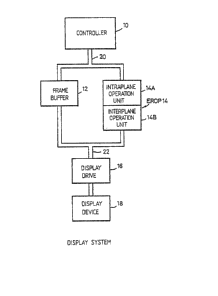
Fig. 1 illustrates a structure of a display system
JA9-35-023
~Z7~3~
according to the presen~ invention. The display system is
providecl with a controller 10, such as a microprocessor,
which controls the entire system, a frame buffer 12 which
comprises a plurality of memory planes and into which image
data to be displayed are written, an extended raster opera-
tion circuitry (EROP) 14 which performs specified raster
operations on the image data in the frame buffer 12, a
display drive 16 7~hich converts ~he images read out o~ the
frame buffer 12 into an appropriate form to be displayed,
and a display device 18, such as a CRT display, which
visually displays the images. The controller 10 writes the
images to be displayed into the frame buf~er 12 and
transfers operation commands to the EROP 14 through a bus
20. Upon receipt of the operation commands, the EROP 14
accesses the frame buffer 12 through a bus 22 and performs
the specified raster operations. The images to be displayed
in the frame buffer 12 are read into the display drive 16
under the control of the controller 10 to receive necessary
processing such as an analog~digital conversion, and then
displayed by the display device 18.
Since the controller 10, the display drive 16, and the
display device 18 are well known and are not directly
related to the present invention, they are not detailed
here.
As illustrated in Fig. 1, the ~ROP 14 is divided into
an intraplane operation unit 14A and an interplane operation
unit 147B~ The intraplane operation unit 14A, which corre-
~9~85-023
l~7 ~
3~
sponds to the conventional raster operation circuits,
performs the operations in each of the memory planes com-
prising the Erame buffer 12. The interplane operation unit
14B, which is a hardware newly provided in accordance with
the present invention, performs the operations between the
memory planes. Although, in the present embodiment, the
frame buffer 12 comprises foux memory planes, the present
invention is not limited thereto, but may also be applied to
other frame buffers comprising different numbers of memory
planes in the similar manner.
The frame buffer 12 and the EROP 14 may conceptually be
interconnected as illustrated by Fig. 2. In the example
illustrated by Fig. 2, the intraplane operation unit 14A
comprises eight raster operation circuits ROP0 - ROP7. A
first group of raster operation circuits ROP0 ~ ROP3 perform
the specified operations on the data from the source areas
in the planes 0 - 3 and predetermined pattern data B0 - B3
so that the respective planes are corresponded. A second
group of raster operation circuits ROP4 - ROP7 perform the
specified operations on the operation results C0 - C3 of the
first group and the data D0 - D3 from the destination areas
in the planes 0 - 3 so that the respective planes are
corresponded~ The operation results E0 - E3 of the second
group are transferred to the interplane operation ~nit 14B,
and the outputs F0 - F3 of the interplane operation unit 14B
are written into the final destination areas or display
areas in the planes 0 - 3.
JA9-85-023
3~27~
The operation of the circuitry illustrated by Fig. 2
may be expressed as follows~
Ci = fj (Ai, Bi)
Ei = fk (Ci, Di~
Fi = fe (E0, E1, E2, E3)
In the above expressions, the i denotes the numbers of the
memory planes and the fj, fk, and fe denote the specific
logical functions, all of which are specified by the con-
troller 10.
In the example illustrated by Fig. 2, although the
intraplane operation unit 14A is followed by the interr
operation unit 14s, their positional relation in hardwa~
may be vise versa. In that case, the interplane operation
unit 14B would receive, as the input, the plane data A0 - A3
from the source areas and the operation results F0 - F3
would be input into the first group of raster operation
circuits ROP0 - ROP3 together with the pattern data B0 - B3.
The pattern data B0 - B3 represent contiguous patterns such
as a checker-board pattern and are suppl1ed from the con-
troller 10 or have been stored in a dedicated pattern memory
(not shown) together with other patterns. The pattern data
also consist of four bits per pixel.
The intraplane operation unit 14A comprises four raster
operation circuits in each group. However, each group may
be replaced by a single raster operation circuit so that the
JA9-85-023
~Z7~
data in different planes may be sequentially supplied
thereto. Further, the intraplane operation unit itself .
be replaced by a single operation circuit.
Fig. 3 illustrates an example of the structure of the
intraplane operation unit 14A. In the illustrated example,
the first and second groups of raster operation circuits are
shown in blocks as "#l ROP" and "#2 ROP," respectively. As
stated above, each group may be replaced by a single opera-
tion circuit. The image data consisting of four bits per
pixel read out of the frame buffer 12 (Fig. 1) are loaded
into a buffer register 30 through the bus 22. In the
present embodiment, it is assumed that one byte of image
data are read out of each of the corresponding stored a~
in the four memory planes of the frame buffer 12. There
fore, the buffer register 30 requires the capacity of at
least four bytes t32 bits). The outputs of the buffer
register 30 are connected to the one inputs of the first and
second groups of raster operation circuits 32 ~#1 ROP) and
34 (#2 ROP). The data A0 - A3 from the source areas are
supplied to the first group 32, while the data D0 - D3 of
the destination areas are supplied to -the second group 34.
A pattern register 36 receives the pattern data con-
sisting of four bits per pixel from the controller 10 or a
dedicated pattern memory (not shown~ and supplies the
pattern data B0 B3 to the other inputs of the first group
of raster operation circuits 32. The outputs of the first
group of raster operation circuits 32 are connected to the
JA9~35-023
~27~3~
other inputs of the second group of raster operation ci~
cuits 34 to supply the operation results C0 - C3 thereto.
The second group of raster operation circuits 34 output the
final operation results E0 - E3 of the intraplane operation
unit 14A and transfer them to the interplane operation unit
14B.
The commands which specify the operations to be per-
formed in the first and second groups of raster operation
circuits 32 and 34 as well as in the respective raster
operation circuits in the interplane operation unit 14B, to
be explained later, are transferred from the controller 10
to a command circuit 38 through the bus 20. Each of the
raster operation circuits performs the operations specified
with operation specifying signals, namely OP codes, from the
command circuit 40. In the present embodiment, the OP
codes, each consisting of four bits, can specify 16 types of
operations, as shown in the following Table 1.
JA9~85-023
~Z7~
Table 1
OP Code Operation
0000 Z = '00' (hexadecima1)
0001 Z = X ~ Y
0010 - Z = X ' Y
0011 , Z = X
0100 Z = X Y
0101 ~ = ~
~-0110 Z = X ~ Y
0111 Z = X + Y
1000 Z = X Y
1001 Z = X
1010 Z = ~
1011 Z = X + Y
1100 Z = X
11~1 Z = X + Y
1110 Z - X + Y
1111 Z = 'FF' (hexadecimal)
In the above Table 1, the X and Y d~note the inputs to
each operation circuit (X denotes the left input and Y
denotes the right input) and tbe~Z denotes the output. Each
of the inputs and output consists of one byte and the
operations are performed so that the respective bits are
corresponded. It would be convenient to render the meanings
of the OP codes shown in Table 1 the same to all of the
operation circuits. To the respective operation circuits in
the interplane operation unit 14B to be described below, the
command circuit 38 transfers plane selection signals togeth-
er with the OP codes. It should be understood that the
JA9~85-023
1-1
number and types of the operations which can be performed in
the present invention are not limited to those shown in
Table 1.
Fig. 4 illustrates a structure of the interplane
operation unit 14B according to the present invention. The
interplane operation unit 14B consists of four operation
circuits 40 IROP8), 42 (ROP9), 44 ~ROP10), and 46 tROPll),
each of which is provided for each of the planes, and four
eight-bit-delay registers 48, 50, 52, and 54, each of ~hich
returns the output of each of the operation circuits back to
one of the inputs thereof with the delay of one cycle. The
one of the inputs of each of the operation circuits is
connected to the output of the related delay register (D),
while the other of the inputs thereof is connected to the
outputs of the second group of raster operation circuits 38.
The operations to be performed by the respective operation
circuits 40 - 46 are specified with the OP codes from the
command circuit 38. To cause the interplane operation unit
14B to operate, the co~mand circuit 38 supplies the plane
selection signals which specify the data of the planes to be
manipulated in the respectl~e operation circuits 40 - 46,
together with the OP codes. Each of the plane selection
signals consists of four bits, each bit corresponding to
each of the different planes, and each of the operation
circuits 40 - 46 receives, as an lnputr the data of the
plane corresponding to 'tl" bit. The selection of the plane
data may be performed with a multiplexer ~not shown), for
example.
JA9-85-023
7~3~
Each of the operation circuits 40 - 46 may be th
as each of the ROP0 - ROP7 illustrated in Fig. 2, excep~
the plane selection, and may be constituted with a
general-purpose operation circuit or a program array logic.
Fig. 5 illustrates an example thereof. The circuit illus-
trated by Fig. 5 performs the operation of the "i"-th bit ~i
= 0, 1, 2, ..., and 7), and therefore, such eight circuits
are required for each of the ROP0 - ROP11. As seen from the
figure, the logical function of the circuit may be
expressed as follows.
Zi = Xi O Yi O OP0 + Xi O Yi O OP1 + Xi O Yi O OP2 +
Xi O Yi O OP3
In the above expression, the Xi, Yi, and Zi denote the
"i"-th bits of the X, Y and Z shown in Table 1, respectively
and the OP0 - OP3 denote the four bits of an OP code to be
supplied from the command circuit 38. In the present
example, oP0 is the rightmost bit of the OP code and OP3 is
the letmost bit thereo. Thus, depending upon whether each
of the OP0 to OP3 is 0 or 1, the operations shown in Table 1
are performed. The details of the operation of the circuit
illustrated by Fig. 5 would not be necessary to be
explained, and therefore, are omitted here.
JA9-85-023
13
~7~3~L
Example 1 : Extraction of Specified Color
In a color display system, it is a basic function to
manipulate the areas of one specific color or the areas of
the other colors on a color image surface. In the prior
art, as disclosed for example by -the applicant's co-pending
commonly assigned CA Patent Application Serial No. 457,027,
filed June 20, 1984, (corresponding to the JapanesP Patent
Unexamined Published Application No. 60 - 50,586 filed on
August 16, 1983), the comparison of colors has been
performed with a dedicated comparator. However, according
to the present invention, this can be easily realized with
general-purpose operation circuits.
Now assume that the bit configuration of a pixel having
a color desired to be extracted in the image written into
the frame buffer 12 is P0 = 1, P1 = 0, P2 = 1, and P3 = 1.
The P0 - P3 denote the four memory planes comprising the
frame buffer 12. Further, assume that the data representing
the areas of the color desired to be extracted are to be
written into the plane 0 (P0).
Fundamentally speaking, the extraction of a color
according to the present invention may be accomplished by
inverting the image data of the planes having the "0" bits
(P1 in the above example) among the four ~its of the pixel
having the specified color, and then ANDing all the planes.
In the present example, the final AND operation results are
written into the plane 0 (P0). For the intraplane operation
unit 14A, the controller lO transfers, to the co~nand
circuit 38, the commands which cause the operation circuit
J~g-85 -023
1~
~2~C~3~
ROPl (or ROP5~ corresponding to the plane 1 (P1) to perform
the operation of Z = X and cause the other operation
circuits to perform the operation of Z = X. In response to
these commands, the command circuit 38 transfe~s the OP code
"1100" to the ROPl (or ROP5), and transfers the OP code
"0011" to the ROP0, ROP2, ROP3, ROP4, ROP5 (or ROPl~, ROP6,
and ROP7. Thus, at the outputs of the intraplane operation
unit 14A, the operation results of E0 = A0, El = A1, E2 =
A2, and~E3 = A3 are obtained. In case that the first and
second groups of raster operation circuits 32 and 34 com-
prise respectively a single operation circuit, the command
circuit 38 supplies the OP codes stated above in an appro-
priate sequence.
For the interplane operation unit 14s, the controller
10 transfers, to the command circuit 38, the commands which
cause the operation circuit ROP8 corresponding to the plane
0 (P0) to perform the operations and plane selections shown
in the following Table 2 and cause the other operation
circuits ROP9 - ROPll to perform the operation of Z = "00."
Table 2
Cycle OP CodePlane Selection
0011 (Z=X) 0001 ~PO)
2 0001 tZ=X-Y)0010 (P1)
3 0001 (Z=X-Y)0100 (P2)
4 0001 ~Z=XY)1000 (P3)
The above Table 2 indicates that the operations of one
byte are completed by four cycles. The operations may be
JA9-85 023
3~
- expressed as follows with the symbols indicated in Fig. 2.
F0 = E0 ~ El ~ E2 E3
If the two dimensional size of the image including the
areas of the specified color is equivalently n bytes, it
would be required to repeat n times the operations of the
four cycles shown in Table 2.
-
Since the ROP9 - ROPll output only the bytes of all
zeros in all of the cycles, the image data including only
the areas of the specified color are finally written into
the final destination area or display area in the plane 0
~P0). In this case, the bit configuration of each pixel
becomes "1000," differing from the original one "1011."
Thus, in the present example, the areas of the specified
color have been extracted by converting the specified color
into another color. If it is desired to extract it without
such a conversion, it may be accomplished by causing also
the ROP10 and ROPll to perform the same operations as shown
in Table 2.
:~ :
Example 2 : Synthesis of Images
In case of monochromatic images, it is possible to
: synthesize more than two:images among the different images
written into the four planes, respectively, only by employ-
ing OR operations~ For example, when the images in ~he
plane 0 and the plane 1 are to be synthesized and written
JA9-85-023
~27~
into the plane 3, the ROP0, ROPl, ROP4, and ROP5 are caused
to perform the operation of Z = X and the ROPll is caused to
select the plane 0 and the plane 1 and perform the opera-
tions of Z = X and Z = X ~ Y.
In case of color images, since only such OR operations
may cause different colors to be produced in overlapping
portions, it would be required to synthesize such images by
giving-priorities thereto. Namely, a color image with a
lower priority is synthesized only in the background area of
another color image with a higher priority. Since the
background area can be extracted with the procedure of
Example l, the background area and the color image with the
lower priority are ANDed, and the results and the color
image with the higher priority are ORed, thereby to obtain a
synthesized image.
:
Particularly, now assume that a color image having four
colors (two bits per pixel) with higher priorities have been
written into the plane 0 and the plane 1 and that another
color image having four colors with lower priorities have
been written into the plane 2 and the plane 3, for example.
When the bit configuration of a pixel in the background area
is "11" and a synthesized image is to be written into the
destination areas in the plane 0 and the plane 1, the
operation circuit ROP10, which corresponds to the plane 2 in
the interplane operation unit 14B, is caused to perform the
operation of F2 = E0 E1 E2, and the operation circuit
ROP11, which corresponds to the plane 3, is caused to
JA9-85-023
~27~
perform the operation of F3 = E0 ~ E1 ~ E3. These l
tions are similar to those shown in Table 2. However, .
three planes are ANDed in this case, only three cycles are
required for each byte. The operation results are written
into the plane 2 and the plane 3, respectively. Next, the
operation circuit ROP8, which corresponds to the plane 0, is
caused to perform the operation of F0 = E0 + E2, and the
operation circuit ROP, which corresponds to the plane 1, is
caused to perform the operation of El = E1 -~ E3, thereby to
obtain a synthesized color imaye. Each of the operation
circuits ROP0 ROP7 in the intraplane operation unit 14A is
specified to perform only the operation of Z = X.
Besides the above, various applications of the present
invention are possible.
Advantages of the Invent on
According to the present invention, it is easily
possible to perform any complex logical operations including
interplane operations with general-purpose operation
circuits.
JA9-85-023