Note: Descriptions are shown in the official language in which they were submitted.
~27~3~
OPTICAL LOGIC ARRANGEME~T
WIT~ SELF ELECTRO-OPTIC EFFECT DEVICES
Technical Field
-
This invention relates generally to optical logic
arrangements and, more particularly, to an optical logic
arrangement having self electro~optic effect devices for
performing an optical logic operation.
Background of the Invention
~ vast number of prior art logic circuits employ
optical devices to perform optical logic functions and
operations. However, many of these circuits involve
converting logic level signals between the optical domain
and another domain such as the electrical domain. This
optical conversion process limits the bandwidth of the
optical signals, requires additional processing time, and
commonly requires additional circuitry. Generally, the
output signal of a nonlinear optical device is a nonlinear
~ gain function of an input signal applied to the device
; 20 where either the input or the output signal is in the
optical domain. In the more specific case of an optically
nonlinear optical device, the input and the output signals
are both in the optical domain. Consequently, optically
nonlinear optical devices can regenerate optical signals
and perform optical logic functions such as the optical
logic NOR, OR, NAND, and the like. Elowever, optically
nonlinear optical devices that employ an optical conversion
process still have the aforementioned problems.
With the use of parallel processing techniques,
it is often desirable to connect in a parallel manner the
optical output of each optical logic element in one array
to the optical input of each optical logic element in
another array. As a result, the number of individual
~; physical connections using, for example, optical fibers
between the two arrays can be enormous with the tokal
equaling the mathematical product of the number o elements
in one array times the number of elements in the other
~ L~
.
:
.; ~
~ ~J~
~ ~t V ~F~
-- 2
array. Depending on the physical size of khe elements as
well as the interconnections, space considerations can
rapidly become a factor limiting the number of connections
between two arrays. This is just one reason why optical
parallel processing techni~ues have had such limited
acceptance and use.
~ nother prior art approach Eor interconnecting
optical logic elements uses a computer-generated
transmission hologram. Generally, a hologram consists of
any material for storing the optical wavefront from an
object that is encoded in an optical fringe pattern for
subsequent recreation of the wavefront. One familiar
example of a hologram for creating artistic visual effects
is a photographic plate that has been exposed to the
coherent light from a three-dimensional object and a
reference beam interfering in the plate. After the
~ photographic plate is developed, the re-Eerence beam is
;~ again passed through the developed photographic plate to
recreate a three-dimensional image of the object.
~ 20 One example of an optical sequentia~ logic system
-~ utilizing computer-generated transmission holograms for
optically interconnecting the optical logic elements of the
system is described by A. A. Sawchuk et al. in Technical
Report No. 1100 entitled "Nonlinear Real-Time Optical
~; 25 Signal Processing", University of Southern California Image
Processing Institute, Los Angelesr California, 1983. The
optical logic system includes an array of computer-
generated Fourier transmission holograms for optically
interconnecting a similar array of liquid crystal light
valves. The light valves are optically nonlinear optical
devices and are operated to regenerate optical signals and
to perform an optical logic NOR function. However, one
disadvantage of the liquid crystal light valve is that the
`~ optical input control signals are received on one surface
of the device and that the optical output signals are
emitted from another surface usually on the other side o
the device. Thus, the transmission holograms and a
' ''~
. .
.
~ ~7 ~J 3 ~_d ~
complicated arrangement of precisely positivned lenses and
mirrors must direct the optical output signals from the
rear surface of the light valve array 360 degrees onto the
front surEace of the light valve array. The long distance
that optical output signals must travel from the rear
surface o a light valve before being reflected as an
input control signal onto the Eront surface of at least one
other light valve, severely limits the operating speed of
any optical system using this transmission hologram
interconnection arrangementO Another problem with this
interconnection arrangement is the mechanical precision
required in aligning the transmission holograms and the
light valves with the mirrors and the lenses. A slight
vibration can misalign the entire system.
Another disadvantage of the liquid crystal light
valve is its relatively slow switching speed. Faster speed
nonlinear Fabry-Perot Interferometers are possible
substitutes for the liquid crystal light valves. However,
with faster switching speeds, proportional amounts of
- 20 additional power are required to operate the device.
Another problem with Fourier transmission
holograms is the significant power loss of an optical
signal as it passes through the hologram. Each optical
signal passing through a ~ourier transmission hologram
forms two images of which only one is used to interconnect
the light valves and has at most half the optical power of
the incident signal. Furthermore, transmission holograms
operate only with coherent light which may result in
optical interference at the input of an optical logic
element due to constructive and destructive interference
between several input signals.
Summar~ of the Inventlon
The foregoing problems of transmission hologram
optical logic arrangements with llquid crystal light valves
or nonlinear interferometers are solved and a technical
advance is achieved by an optical logic arrangement
comprising self electro-optic effect devices optically
-- 4
interconnected by a reflection hologram. Each device is
responsive to a control light beam for emitting an output
light beam. In response to interconnecting output light
beam from one self electro-optic effect device, the
reflection hologram originates an interconnecting control
light beam to another self electro-optic effect device.
The reflection hologram can also be made to originate
individual interconnecting control light beams ~o ~wo or
more self electro~optic effect devices in response to an
interconnecting output light beam from one device~
Advantageously, with each self electro-optic
effect device operated to perform an optical logic
function, a plurality of these low-power, high-speed self
electro-optic effect devices may be optically interconnected
to form an optical logic circuit or to perEorm an optical
logic operation.
On the other hand, the invention in its broad
scope includes an optical sequential logic arrangement
comprising: a self electro-optic effect logic element
responsive to a first and a second control light beam
for emitting an output light beam, said output beam being
a nonlinear gain function of at least one of said first
and second control beams; and a reflection hologram
responsive to said output light beam from said self
25 ~ electro-optic effect logic element for reflecting a
predetermined amount of said output light beam back to
said self electro-optic effect logic element as one of
said ~irst and second control light beams.
In one illustrative embodiment of this invention,
the reflection hologram originates an interconnecting
; control light beam to a designated self electro-optic
effect device by reflecting a predetermined amount of the
interconnecting output light beam from a specified self
electro-optic effect device to the designated device.
~i ,
' ' . :
: `' ''- `' :
~27~3~3
- 4a -
In another illustrative embodiment of this
invention, a plurality Qf reflection holograms positioned
in a two-dimensional array optically int~rconnects a
plurality oE self electro-optic effect de~vices to form a
two-by-two optical crossbar switch. Each device is
operated to function as optical logic NO~ gate.
In accordance with one feature of this invention,
each self electro-optic effect device is responsive to
control light beams incident on either surface of the two-
dimensional device array for emitting an interconnecting
ou~pu~ light beam to a specified reflection hologram.
Advantageously, without the use of mirrors or
lenses, each reflection hologram directly reflects the
interconnecting output light bea~ from a ~pecified selr.
electro-optic effect logic element to at least one other
~1
~7~
- 5
self electro-optic efEect logic element to form the optical
crossbar switcho Since cumbersome arrangements of mirrors
or lenses are no-t required, optical logic systems and
optical signal processing can be simplified substantially.
Furthermore, the self electro-optic effect logic elements
may be op~ically in-terconnected in a relatively small
space. Since intersecting light beams do not interfere
with one another, the self electro-optic effect logic
arrangement significantly enhances the practical use of
~.
optical parallel processing techniques.
In accordance with another aavantage of this
invention, the optically nonlinear self electro-optic
effect devices oE this invention can switch at a higher
speed than a liquid crystal light valve and at low
switching power levels. Thus, this optica] logic
arrangement is ideally suited for use with low optical
power light sources. Furthermore, the use of the self
electro-optic effect devices of this invention also
minimizes the generation of undesired heat at high
switching speeds normally associated with high speed
optical devices.
In accordance with another feature of this
invention, the reflection holograms can be made to feed
back any number of interconnecting light beams to Form a
sequential optical logic circuit.
Another advantage of this invention is that the
reflection hologram functions with either coherent light
or incoheren-t light from inexpensive low-power light
sources. This significantly reduces the cost of an optical
logic system as compared to a transmission hologram optical
logic system that uses only coherent light from normally
higher cost laser light sources.
In accordance with still another feature, the
arrangement further comprises director means such as a
rainbow transmission hologram and a planar mirror for
; directing control light beams between the optical logic
~ element array and other optical sources and receivers.
.
~ ' . ~, .
~2~ 3
In accordance with yet another feature o this
inve~tion, with the use of optically nonlinear self
electro-optic effect devices that receive optical control
signals on either side o a device array, combinational and
sequential optical logic circuits can easily be
interconnected in a relatively small space to orm even
larger and more complex optical logic circuits and systems
such as an optical digital processor.
Brie~ Description of the Drawings
The invention may be better understood from the
ollowing detailed description when read with reference to
the drawing in which:
FIG. 1 depicts an illustrative arrangement for
optically interconnecting a plurality of optically
; 15 nonlinear optical devices;
FIG. 2 shows the illustrative arrangement of
~ FIG. 1 with a rainbow transmission hologram and a planar
; mirror for directing external optical signals to and from
~ the device array, respectively;
- 2~ FIG. 3 depicts a diagram of an illustrative
optically nonlinear optical device known as the self
electro-optic effect device (SEED) thay may be operated to
~ function as an optical logic NOR gate;
: FIG. 4 graphically depicts the theoretical output
power of the SEED of FIG. 3 as a function of optical input
power in the bistable region of the device;
FIG. 5 graphically depicts the empirical
responsivity S(~) of an exemplary diode structure that may
be used ~or the SEED of FIGo 3;
FIG. 6 graphically depicts the entire theoretical
input-output power characteristics of the SE~D of FIG 3;
FIG. 7 graphically depicts the empirical input-
output power characteristics and bistable switching
operation o a sample SEED;
FIG. 8 depicts an illustrative arrangement for
~ forming optical fringe patterns in a photographic emulsion
-- to optically interconnect an array of optically nonlinear
~,~
~ ' .
.: . .
, ~ :
~27~3~3
optical devices;
FIG. 9 depicts an illustrative arrangement for
generating and directing coherent light beams to form the
optical fringe patterns of FIG. 8;
FIG. 10 depicts an illustrative logic diagram of
a well-known two-by-two crossbar switch comprised of only
NOR gates;
FIG. 11 is a nodal diagram of the crossbar switch
of FIG. 10 positioned in a four-by-four array;
~- 10 FIG. 12 depicts an illustrative two-by-two
optical crossbar switch corresponding to the crossbar
switch of FIG. 10;
FIG. 13 depicts a rear pictorial view of the
illustrative interconnection arrangement of FIG. 2 showing
selected optical signals as plane waves;
FIG. 14 shows an illustrative logic diagram of a
- well-known clocked JK flip-flop comprised of only logic NOR
; gates;
FIG. 15 is a nodal diagram of the clocked JK
flip-flop of FIG. 14 positioned in a three-by-three array;
FIG. 16 depicts an illustrative optical
sequential logic arrangement comprising optically nonlinear
.'! self electro-optic efect devices for implementing an
optical version of the clocked JK flip-flop of FIG. 14;
FIGs. 17, 18 and 19 illustrate the operation of a
Fabry-Perot Interferometer; and
FIGs. 20 and 21 illustrate the operation of a
nonlinear Fabry-Perot Interferometer.
Detailed Description
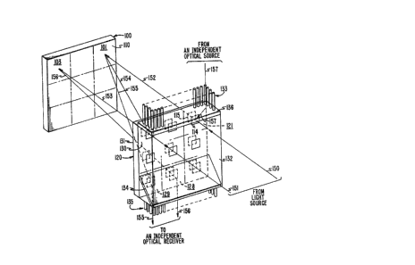
~epicted in FIG. 1 is an illustrative arrangement
for optically interconnecting a plurality of optically
nonlinear optical devices 121 through 129 positioned in a
two-dimensional array 120. As known in the art, the
optical output signal of an optically nonlinear optical
device is a nonlinear gain function of at least one optical
input signal applied to the optically nonlinear optical
device. Consequently, an optically nonlinear optical
.
.
-- 8 --
device can regenerat~ optical signals and perform optical
logic functions. Bias light beams 150 and 151 optically
bias respective optically nonlinear optical devices 121 and
123 in a well-known manner to function as optical logic
elements such as optical NOR gates. The optical
interconnection arrangement comprises re~lection
hologram 100 orl more particularly, a plurality of
re1ection subholograms 101 through 109 similarly
positioned in a two-dimensional array. In response to an
~ 10 in-terconnecting optical output signal such as
: interconnecting output light beam 152 received in a
predetermined direction from the rear surface 131 of a
specified device such as 121, the correspondingly
positioned subhologram such as 101 originates one or more
individual interconnecting control light beams such as 154
and 155 each in a different predetermined direction back to
` the rear surface of one or more other devices such as 123
and 129 in the device array. For example, to optically
interconnect three optically nonlinear optical devices such
as 121, 123, and 128 in series, the position of each
; emitting device such as 121 and 123 is maintained in a
fixed position relative to its correspondingly positioned
subhologram such as 101 and 103, respecti~ely. Otherwise,
two optically interconnected optically nonlinear optical
devices need only be positioned in a ~ixed direction from
the correspondingly positioned subhologram. Optically
nonlinear optical devices 121 through 129 have front and
rear surfaces 130 and 131 for receiving optical signals
propagating in either one of two generally opposing
directions. Thus t a plurality o~ holograms such as
subholograms 101 through 109 can be made to interconnect
`~ these two-surfaced optically nonlinear optical devices to
~orm any combinational or sequential optical logic circui~.
As suggested, each optically nonlinear optical
device in array 120 is responsive to light beams received
on either one or both o~ front and rear suraces 130 and
131 for emitting an interconnecting output light beam from
., . ~ ,
'. ~
' '
-,:,: , '
~27~3~
g
one of the two surfaces. The wavelength of these optical
signals or light beams can range from the ultraviolet to
the infrared~ Several optically nonlinear optical devices
such as the nonlinear Fabry-Perot Interferometer and the
self electro-optic effect device (hereinafter refer~ed to
as SEED) that will be described hereinafter are suitable
for use as the optically nonlinear optical device. In
addition, each of these optically nonlinear optical devices
may be operated to function as an optical logic element
such as an optical NOR gate.
Each optically nonlinear optical device in
~; array 120 is in either one of two transmission states
depending on the power of the incident light. When the
power of an incident light beam is below a predetermined
threshold level, the device is in a first transmission
state and simply passes or, more particularly, receives the
incident light beam and emits an output light beam. For
example, a source of either coherent or incoherent light
(not shown) illuminates the front surface 130 of array 120
with optical bias signals such as bias light beams 150 and
151. The bias beams cause respective optically nonlinear
optical devices 121 and 123 to function as optical logic
NOR gates. When the power of bias beam 150 is just below
the threshold level of ~OR gate 121, the gate passes bias
beam 150 as a high logic level output light beam 152 to
reflection subhologram 101. Similarly, NOR gate 123 passes
bias light beam 151 as a high logic level output light beam
153 to reflection subhologram 103.
In contrast to transmission holograms,
reflection holograms reflect, rather than pass, optical
signals. In response to interconnecting output beam 152,
reflection subhologram 101 originates interconnecting
control light beams 154 and 155 to respective optically
nonlinear optical devices 123 and 129. Macroscopically,
reflection subhologram 101 originates in~erconnecting
cont~ol beams 154 and 155 by splitting and reflecting
output beam 152. As a result, reflection subhologram 101
:: .
~27~
- 10 -
optically connects optically nonlinear optical device 121
to optically nonlinear optical devices 123 and 129. Since
the front surface 110 of reflection subhologram 101 and the
rear surface 131 of optically nonlinear optical device 121
are positioned in a substantially parallel manner directly
facing each other, subhologram 101 receives interconnecting
output beam 152 in a direction having a zero degree angle
of incidence 170 with respect to the normal 169 of front
surface 110. The direction of interconnecting output light
beam 152 would change, and the incident angle would, of
coursel increase if the two opposing surfaces of
subhologram 1Q1 and optically nonlinear optical device 121
were either not parallel or did not directly face each
other.
A reflection hologram can originate any number of
interconnecting control light beams and originate each one
' in a di~ferent direction. Thus, as illustrated, control
ht beams 154 and 155 propagate in different directions
to respective optically nonlinear optical devices 123 and
129 and in a direction generally opposite to that of
interconnecting output beam 152. The total optical power
of the reflected interconnecting control beams 1S4 and 155
will, of course, be somewhat less than the power of the
interconnecting output light beam 152~
Similarly, reflection subhologram 103 reflects
interconnecting output beam 153 received from optical NOR
gate 123 as interconnecting control beam 156 to optically
nonlinear optical device 128. Without a bias beam incident
on optically nonlinear optical devices 128 and 129, a low-
power level interconnecting control beam normally passes
straight through the optically nonlinear op-tical device.
When bias beam 151 and high logic level
interconnecting control beam 154 are both incident on NOR
~; gate 123, the power of the incident light beams exceeds the
predetermined threshold levsl of the optically nonlinear
optical device and causes the device to assume a second
transmission state~ In this second state, the optically
~ .:
. .
.: ''- .
;.
,:
~.
~27~3~3
nonlinear optical device either absorbs a significant
portion of the incident light or reflects the incident
light depending on the type of device used. As a result,
interconnecting output beam 153 from NOR gate 123 and
reflected interconnecting control beam 156 from reflection
subhologram 103 assume a low logic level~
In addition, optical control signals other than
those from hologram 100 such as a high logic level control
beam from an independen~ optical source such as another
; 10 optical logic circuit (not shown) may be used to control
the state of any device in the array. For instance, a
p1urality of optical control signals ~ransmitted via a
fiber optic bundle can be individually directed to specific
array devices by, for example, a well-~nown rainbow
transmission hologram. To further illustrate this point,
FIG. 2 shows another view of the illustrative optical
interconnection arrangement of FIG. 1 with rainbow
;~ transmission hologram 136 for directing control beam 157
from an independent optical control source to optically
nonlinear device 121.
Well-known rainbow transmission hologram 136 is
maintained in a position perpendicular to surface 130 of
~ device array 120 by any suitable transparent material 132
; such as silicon glass or sapphire. The transparent
material maintains the rainbow hologram and device array
in a fixed perpendicular position and readily passes bias
beam 150 and control beam 157 to reach optical receiving
and emitting area 114 of device 121. One of the ~ibers in
bundle 133, which is attached to the rainbow hologram in a
suitable manner, guides the control beam from the
independent optical ontrol source to the rainbow hologram.
Rainbow hologram 136 then redirects or, more particularly,
passes the control beam therethrough to device 121. By way
of example, when high logic level control beam 157 and
optical bias beam 1S0 are both incident on front surface
130 of the array, device 121 absorbs the incident light,
and interconnecting output beam 152 along with associated
,~
:
: ' '
~ ` ' , ;''' . ~ ' ' ~
7~3~
- 12 -
interconnecting control beams 154 and 155 assume a low
logic level. Again, depending on the type of optical
device used, a low logic level optical signal may be either
the absence of light or an optical signal significantly
attenuated with respect to a high logic level optical
signal.
Control light beams from the device array to an
independent optical receiver are emitted by, again, simply
passing a control beam from a reflection subhologram
through an optically nonlinear device in the array when a
bias beam is not incident on the device. As shown,
optically nonlinear optical device 129 passes
interconnecting control beam 155 from reflection
subhologram 101 to an independent optical receiver such as
another optical logic circuit. Likewise, optically
nonlinear optical device 128 passes interconnecting control
beam 156 from reflection subhologram 103 to the independent
receiver. In addition, light beams rom the array may be
directed to the independent optical receiver by the use of
a planar mirror 134 and another optical fiber bundle 135 as
shown in FIG. 2. The transparent material positions and
maintains the mirror with respect to optically nonlinear
optical devices 128 and 129 so that it directs or, more
particularlyr reflects each of light beams 155 and 156 to a
particular fiber in the bundle. The bundle is, again,
affixed to khe transparent material in a suitable manner.
Only a single line was utilized in FIG. 1 and 2
to depict each of light beams 150 through 157. ~owever,
each optical signal approximates a plane wave or, more
particularly, either a very sliyhtly diverging or
converging spherical wave, depending on the direction in
which the wave is traveling with respect to the device.
Depicted in FIG. 13 is a rear pictorial view of the
interconnection arrangement of FIG. 1 illustrating each one
of light beams 150-152~ 154 and 155 as a plane wave.
Recall that reflection subhologram 101 optically
interconnects optically nonlinear devices 121, 123r and
~,.
,: .,~ :
. ' '. . " -
~27~3~3
- 13 -
129.
In this illustrative embodiment, the optical
receiving and emitting areas of each optically nonlinear
device have been formed into a rectangle. As shown in
FIG. 13, when cylindrically-shaped bias beam 150 is
received, the front surface 130 of device 121 i5
illuminated. Of course, only the rectangular receiving and
emitting area 114 of optically nonlinear optical device 121
~is responsive to the cylindrically-shaped bias beam 150.
`~10 When emitted from the rectangular receiving and emitting
area 115 of rear surface 131 of optically nonlinear optical
~;device 121, interconnecting output beam 152 approximates a
rectangular-shaped plane wave that diverges slightly in a
well-known manner to illuminate a predetermined area of
front surface 110 of reflection subhologram 101. In
response to interconnecting output beam 152, subhologram
101 originates rectangularly-shaped interconnecting control
beams 154 and 155 that converge slightly on optically
nonlinear devices 123 and 129, respectively.
Interconnecting control beams 154 and 155 converge in the
opposite manner than the coherent light beams previously
diverged from optically nonlinear optical devices 123 and
129 in forming subhologram 101. This divergence is similar
to that of interconnecting output light beam 152.
Reflection subhologram 101 reflects in-terconnecting control
beams 154 and 155 from the same area of front surface 110.
Since a reflection hologram can be made to
reflect an optical signal in any one or more of a plurality
of predetermined directions, reflection hologram 100 can be
-~ 30 made to optica~ly interconnect the devices of the array in
any desired combination. Furthermore, since only logic NOR
~- gates are needed to form any combinational or sequential
::
logic circuit or any combination thereof, the re~lection
hologram may be made to optically interconnect an array of
optical logic NOR gates to form any desired combinational
or sequential optical logic circuit that utilizes all
optical information signals. Not only does this optical
.
. .
: .
. , , ~.
,,, , "
27~3~
interconnection arrangement facilitate serial data
processing but, in addition, facilitates parallel
processing in which large numbers of parallel-connected
optical logic elements may be accessed at the same time.
Depicted in FIG. 3 is a diagram of one
illustrative optically nonlinear optical device, which may
be used for devices 121 through 129, comprising a multi-
quantum well (MQW) structure known as a self electro-optic
effect device (SEED). The SE~D Eunctions as a modulator
and photodetector and may be operated to function as a
logic element such as an optical logic NOR gate. The SEED
requires very little switching energy with respect to other
bistable devices such as the nonlinear Fabry-Perot
Interferometer, which may also be used for optically
nonlinear optical devices 121 through 129. Empirically,
the optical switching energy of the SEE~ was found to be
approximately 4 femtojoules/square micron, and the total
switching energy including electrical energy was found to
be approximately 20 femtojoules/square micron. A SEED
having a large photosensitive area of 28,000 square microns
~'~ was found to have switching energy of appro~imately 1.0-1.5
nanojoules. SEEDs having smaller photosensitive areas
will, of course, have lower switching energies and faster
- operation. The self electro-optic effect device is
; 25 described in an article by D. A. B. Miller et al., entitled
"A Novel Hybrid Optically Bistable Switch: The Quantum
Well Self Electro-Optic Effect Device", Appl_ed Physics
Letters, Volume 44, Number 1, July 1, 1984. However, the
SEED will be briefly described herein 50 as to enable the
reader to better understand the operation of the SEED with
respect to FIGs. 3 through 7
As shown in FIG. 3~ the SEED includes a layered
multi-quantum well (MQWj 201 in the intrinsic (i) region
of reverse-biased positive-intrinsic-negative (p-i-n) diode
structure 202. A mul-ti-quantum well structure has a
plurality of thin, narrow bandgap layers interleaved with
a plurality of thin, wide bandgap layers. The narrow
~7~3~3
bandgap layers are sufficiently thin that quantum effects
are evident, and important, in the carrier eneryy levels.
With photon sources having .8 .9 micron wavelengths, the
layers may be comprised of well-known compounds such as
A1GaAs/GaAs. However, other group 3,5 compounds such as
InGaAsP and InGaAs/A1Is may be used with photo sources
having 1.3-1.5 micron wavelengths. This multi-quantum well
diode structure is described in detai] in an article by T.
H. Wood et al., entitled "High-Speed Optical Modulation
with GaAs/GaA1As Quantum Wells in a P-I-N Diode
Structure", Applied Physics Letters, Volume 44, Number 1,
January 1, 1984, at page 16. When an electric field is
perpendicularly applied to the layers of the structure,
i.e., parallel to the small dimension of the layers, the
absorption band edge including any exciton resonance peaks,
can be shifted to lower photon energies. In only microns
of material, changes in optical absorption of 50 percent
can be readily achieved. These optical absorption changes
may be used to make an optical modulator that operates at
room temperature and is compatible with present laser diode
powers, wavelengths, and materials. The absorption is
greatly enhanced relative to the shifts seen in bulk
materials because of carrier confinemen-t in the quantum
wells. A1GaAs multi-quantum wells also show exceptionally
strong room temperature exciton resonances, which enhance
the absorption effects at the band edge. Furthermore, the
use of a p i-n doping scheme in this structure allows the
application of a moderately large electrîc field to the
; active layers without high voltage or current drive. The p
and n layers must have bandgaps so that these layers do not
absorb the incident light. Applying this electric ield to
a reverse-biased diode structure, the structure is also an
efficient photodetector.
The principles of optical absorption exhibited by
the SEED are: first, that increasing the intensity of an
input light beam increases the optical absorption
coefficient of the device; and second, that increasing the
~2~3C~3
- 16 -
absorption of light energy by the device also increases the
optical absorption coefficient~ As a consequence of these
two principles, the SEED swltches nonlinearly between two
optical state~ of transmission. This will be better
understood from the following description of device
operation.
Constant bias voltage supply 203 and positive
feedback resistor 204 are serially connected to p-i-n diode
struc~ure 202 to form the optically nonlinear self electro~
optic effect device. To make the SEED switch, the incident
wavelength is chosen to be near the exciton resonance
position for zero voltage across the diode. With a low
power level light beam 250 incident on the multi-quantum
well diode structure, nearly all the voltage of constant
potential 203 is applied across the diode structure, as
; there is very little, if any, photocurrent in the circuit.
Increasing the optical input power increases the
photocurrent, thereby increasing the voltage drop across
resistor 2a4 and reducing the voltage across the diode.
~` 20 ~his reduced voltage causes increased optical absorption as
the exciton resonances move back, resulting in ~urther
increased photocurrent and consequently leading to
regenerative eedback and switching.
The theoretical optical output power of the SEED
of FIG. 3 under variations in power of an input light beam
such as 250 i5 graphically shown in FIG. 4. Note that, in
the following discussion, the units of beam power are used
rather than intensity. Beam power is expressed in units of
watts and beam intensity in units of watts per square
~ 30 meter. Beam power is the integral of intensity over a
;;~ cross section perpendicular to the axis of the light beam.
Units of power are more useful in the following discussion
because the SEED responds to beam power and, more
particularly, to absorbed beam power. In FIG. 4, the power
of the input light beam is plotted along the horizontal
axis. Along the vertical axis the power oE the output
light beam such as 251 of FIG. 3 is plotted as output
.. . .
,, ': '
, ,
3~3
- 17 -
power. At an input power of value A, the output power is
given by a value of TA. As the input power is increased to
a value of B, the output power increases to a value of TB1.
However, the absorption coefficient of the SEED increases
with increasing input power, and therefore the transmission
curve 320 from input power A to input power B is be]ow a
line of constant slope such as straight line 321. A
further increase of input power from value B to value C
results in a further increase in the absorption coefficient
so that the SEED becomes unstable and switches from a value
of TC1 to a value of TC2. A further increase of input
power to a value of D leads to an output power value of
TD.
Decreasing the power of the input light beam from
input power level C results in the output power tracing
along curve 320 to input power B/ whereupon the absorption
coefficient of the SEED switches to a smaller value, and
the output power increases from TB2 to the value TB1. The
SEED is said to exhibit optical bistability because it
switches from a state of high transmission to a state of
low transmission as the optical input power is increased,
and switches back to a state of hiyh transmission as the
optical input power is decreased. However, optical
bistability may exist for other sequences of switching.
The empirical responsivity S(V) of an exemplary
p-i-n diode structure that may be utilized for diode 202 is
depicted as curve 330 in FIG. 5. The responsivity S(V) is
the photocurrent produced per unit of incident light power,
and ls expressed in the units of amperes per watt (A/W) of
incident light power. Curve 330 shows the measured
(external) responsivity S(V) of the exemplary diode
structure as a function of reverse bias, this measurement
being made with a Iaser light source tuned to a photon
energy of 1.456 eV (851.7nm). This photon energy is
approximately the heavy hole resonance energy at conditions
o zero bias for the MQW structure used. As the reverse
bias is increased, the responsivity first increases as
~;~7~
- 18 -
photocurrent collection becomes complete, and then
decreases as the exciton absorption peak moves to lower
energy. The "bump" between 8 V and 16 V in curve 330 is
due to the light hole exciton resonance similarly moving
past the measuring wavelength.
The input-output power characteristic of the
exemplary diode structure when connected in series with a
positive feedback resistor and a positive source of
potential, as shown in FIG. 3, may be calculated by solving
two simultaneous equations. The first equation involves
the measured responsivity S(V) of the MQW diode structure
as shown in FIG. 5 by curve 330 where;
S = S(V) ( 1 ) .
The second equation is V = VO -RSP where P is the optical
input power, R is the resistance of the Eeedback resistor,
VO is the voltage of the constant bias voltage supply,
and V is the voltage across the diode. This equation may
also be written as:
: V --V
Sa____ (2,.
; The graphical solution is straightforward wi~h equation 2
giving dashed straight lines A, B, C, and D in FIG. 5 of
decreasing negative slope for increasing P. Bistability
results from the multiple intersections of a straight line
and curve 330. Straight lines A and D intersect curve 330
only once. Straight lines B and C have tangent points 331
and 332 with curve 330. The tangent points 331 and 332
represent unstable switching points. All straight lines
between lines B and C have three intersection points with
curve 330, the middle intersection point representing
unstable operation~
The responsivity S and voltage V across the diode
may also be calculated as a function o P by choosing V,
deducing S from equation 1, and P from equation 2. For
reverse bias equal to or greater than 2 volts, optical
absorption closely follows the responsivity. However, to
make a more accurate calculation, the OlltpUt power
. .
3~3
- 19 -
PoUt ( ~ PT ) for each value of diode voltage V and
optical input power P can be deduced from the measured
transmission T(V). Hence, the whole theoretical input-
output power characteristic of a sample SEED as graphically
depicted in FIG. ~ may be derived.
The empirical input-output power characteristic
410 of a sample SEED is shown in FIG. 7. The optical
output power of the device increases along curve 410 until
the input power reaches predetermined input threshold level
401. At this level, the positive feedback causes the
device to become unstable, and the optical output power
~; rapidly switches from output level 402 to lower output
level 403. At this lower output power level, the diode
~ structure absorbs approximately half of the incident light.
; 15 Further increasing the incident light power above input
level 401 causes the output power level to again increase
but at a rate less than the prior rate. Reducing the
incident light power below input level 401 will accordingly
decrease the output power of the device. Thus, at second
~20 predetermined input power level 404, the device once again
becomes unstable, and the optical output power switches to
a higher output power level on curve 410.
With this bistable optical output condition~ it
should be readily apparent that the self electro-optic
effect device (SEED) can be optically biased to function as
an optical logic NOR gate. As shown in FIG. 7, a constant
optical bias signal such as a light beam that has incident
input power level 405 just below predetermined input
threshold level 404 optically biases the SEED to a point
below the knee 406 on input-output power characteristic
curve 410. With just the bias beam incident on the
device, the optical absorption of the diode structure is
; low, and most of the bias beam is consequently passed
therethrough. When additional light such as a control
light beam is incident on the device, the combined incident
optical power is greater than input threshold level 401,
and the optical output power of the device switches to a
:
:::
~2~ 3
- 20 -
lower ou-tput level such as 403. Since any one of a number
of optical control signals in combination with the bias
signal can cause the optical output power of the device to
switch to a lower transmission level, the SEED functions as
an optical logic NOR gate. When all optical control
signals are extinguished, only the optical bias signal is
incident on the device, and the optical output signal
returns to a higher output power level on the curve.
Although the sample device exhibits a hysteresis-
like operation between the two stable transmission states,
~;~ the hysteresis-like effect may be minimized by the use of a
light source having photon energies as suggested and
described in an article by D.A.8. ~iller et al., entitled
"Optical Bistability Due to Increasing Absorption", Optics
Letters, Vol. 9, No. 5, May 1984, at page 162. The
hysteresis-like operation is also a function of the
constant bias voltage supply ~0 and can be also minimized
by selecting V0 so as to intersect the responsivity curve
330 as shown in FIG. 5 only once over the operating range
of the device. In addition, it is reasonably expected that
~ optical absorption in excess of 80 percent will be readily
- obtainable.
Other bistable optically nonlinear optical
devices such as the nonlinear Fabry-Perot Interferometer
may also be used for optically nonlinear devices 121
through 129. The nonlinear Fabry-Perot Interferometer
reflects rather than absorbs incident light. Having
switching speeds comparable to the SEEDI the nonlinear
Fabry-Perot Interferometer requires significantly higher
switching power with the optical signals supplying all the
power. Like the SEED, the nonlinear Fabry-Perot
Interferometer may be optically biased to func-tion as an
optical logic element such as an optical NOR gate.
Furthermore, the nonlinear Fabry-Perot Interferometer
receives incident optical control signals on either of the
two major array surfaces and emits an optical output signal
fro~ one of the same two surfaces. However as suggested,
.:
". ~
: :
.
, . .
~27~3.~; 3
= 21 -
the switching power and energy of the nonlinear
interferometer are considerably higher than those of the
SEED. In addition, the nonlinear interferometer responds
only to coherent light. A detailed description of the
nonlinear Fabry Perot Interferometer is described by D. A.
B. Miller in an article entitled, "Refractive Fabry-Perot
Bistability with Linear ~bsorption: Theory of Operation
and Cavity Optimization", IEE~ Journal of ~uantum
Electronics, Vol. QE-17, No. 3, March 1981. Another
description of the nonlinear Fabry-Perot Interferometer for
use as an optical logic element is described by J. L.
Jewell, et al. in an article entitled, "Use of a Single
Nonlinear Fabry-Perot Etalon as Optical Logic Gates",
- Applied Physics Letters, Vol. 44, No. 2, January 15, 1984,
; 15 at page 172.
FIGs. 17 through 19 illustrate the operation of a
linear Fabry-Perot Interferometer 1301. Basically, the
interferometer comprises a cavity 1302 with front and rear
walls 1303 and 1304. For example in the general case
illustrated in FIG. 17, 90~ of incident light beam 1350 at
front wall 1303 is reflected as reflected output beam
1351. The remaining 10% of the incident beam is refracted
as forward beam 1352. The refracted forward beam (10%)
that enters the cavity is again divided with 90% being
reflected as reverse beam 1353 (9%) and 10% again being
refracted as transmitted output beam 1354 (1%). In FIG.
18, the length of the cavity is such that the forward and
the reverse beams destructively interfere to form resultin~
wave 1355. The power of the transmitted output beam in
this case is less than one percent of the incident light
power. In FIG. 19, the length of the cavity is such that
the forward and the reverse beams constructively interfere
to form resulting wave 1356. Here, the power of the
transmitted output beam is nearly 100% of the incident
light beam with little, if any, power being reflected from
front wall 1303.
In FIG. 20, the operation of a nonlinear Fabry-
. '. .
~27~!3
- 22 -
Perot Interferometer 1401 is illustrated. Here, the cavity
1402 of the interferometer is filled with a nonlinear
material 1405. The index of refraction of this nonlinear
material and consequently the optical path length of the
material in the cavity varies as a function of the incident
light power. Utilizing this property, the optical path
length of the nonlinear interferometer is chosen such that
little, if any, optical power is transmitted when the power
of the incident light is below a threshold level. When the
incident light power exceeds the threshold level/ the index
of refraction and the optical path length of nonlinear
material 1405 change to transmit nearly 100% o~ the
incident light power. Like the linear interferometer
depicted in FIGs. 17 through 19, there are two output beams
from the nonlinear interferometer that are of interest: a
reflected output beam 1452 and a transmitted output beam
1453.
In FIG. 21, exemplary input-output optical power
curve 1410 graphically illustrates the optical output power
of nonlinear interferometer 1401 as a function of the
optical input power. This input-output curve will be used
to illustrate how a nonlinear interferometer may be
operated to perform an optical logic NOR function.
Returning to consideration of FIG. 20, an optical bias beam
1450 with input power level 1460 biases the nonlinear
interferometer to a point on its input-output curve as
illustrated in FIG. 21 that will cause reflected output
beam 1452 to rapidly change from high logic output power
; level 1461 to low logic output power level 1462. The
additional power to raise input power level 1460 to level
1463 is provided by high logic level control light beam
1451. When high logic input power level control beam 1451
and bias beam 1450 are incident on the interferometer,
reflected output beam 1450 assumes low logic output power
level 1462. When bias beam 1450 and only low logic input
power level control beams are incident on the device, the
reflected output beam is at high logic output power level
. . .
...., ~ . .
' ~ - ,
~7~3~t3
- 23 -
1461. Thus, nonlinear interferometer 1401 operates as an
optical logic NOR gateO In addition, transmitted output
beam 1453 may be utilized so that the nonlinear
interferometer performs an optical logic OR function.
Still another optically nonlinear device is the
liquid crystal light valve that can only receive optical
control signals on a front surface and emit an optical
output signal from the rear surface. Such a device could
be used to implement the present invention. However,
appropriate apparatus would have to be positioned so as to
direct the optical output signal to the reflection hologram
and then onto the front surface of the valve.
The reflection hologram of the present invention
optically interconnects nonlinear optical devices and~ in
;~15 particular, optically nonlinear optical devices that are
~;operated to function as optical logic NOR gates. A
plurality of reflection holograms may be made to
interconnect these optical logic gates optically to Eorm
any desired optical logic circuit.
A detailed description of reflection holograms is
discussed by H. J. Caulfield, editor, in the Handbook of
Optical Hologra~y, Academic Press, 1979, and by Collier et
al. in Optical Holography, Academic Press, 1971. In
addition, a series of articles edited by T. H. Jeong for
making reflection holograms may be found in the Proceedings
of the nternational Symposium on Display Art Holography,
Holography Workshops, Lake Forest College, Lake Forest,
Illinois, 1982. Making reflection holograms is generally
well known in the art. However, a description of how to
make a reflection hologram of the present invention such as
reflection hologram 101 for optically interconnecting
nonlinear optical devices will be given next.
Depicted in ~IG. 8 is an illustrative arrangement
for forming and storing optical fringe patterns in a
photosensitive material such as a photographic emulsion for
optically connecting nonlinear optical device 121 to
devices 123 and 129. ~n unexposed photographic emulsion
.
~7~
- 24 -
500 and a plurality of optically nonlinear optical devices
121 through 129 are affixed in a well-known ~anner to the
parallel surfaces 503 and 504 of optically transparent
material 505. For example, the optically transparent
material may be silicon glass or, preferably, a high
thermal conductivity material such as sapphire. The
optically transparent material maintains the nonlinear
devices positioned in a two-dimensional array and
photographic emulsion 500 in a fixed relative parallel
position during ~oth exposure of the photographic emulsion
and after processing when the fringe patterns have been
permanently stored in the emulsion. The index of
refraction of the transparen-t material is selected to
reduce Fresnel reflections. However, as suggested, a
sapphire material is preferred because it more evenly
distributes the heat generated by the optical signals
passing therethrough~
Also included in the recording arrangement are
spatial light modulator masks 501 and 502 such as well-
known electrically operated magneto-optic arrays that are
temporarily affixed to rear surface 111 of the unexposed
photographic emulsion and front surface 130 of the device
array, respectively. As shown in FIG. 8, coherent light
beam 551 passes through mask 501 along with coherent light
beams 552 and 553 through mask 502 to illuminate outside
surface 111 of photographic emulsion 500 and outside
surface 130 of devices 123 and 129, respectively.
FIG. 9 depicts the derivation of coherent light
beams 551 through 553 from a single coherent beam.
Coherent light beam 570 from a coherent light source 520
such as a commercially available laser is split into two
coherent light beams 551 and 571 by commercially available
variable beam splitter 521. One or more light beam
directors such as mirrors 522 and 523 are positioned to
- 35 direct coherent reference beam 551 to illuminate a
:
predetermined area of emulsion 500 designated ~or
reflection subhologram 101. Coherent beam 571 is split
..... .
,
.
c~3
into two equal-power coherent object light beams 552 and
553 by another beam splitter 524. In this illustrative
embodiment, object beams 552 and 553 have half the optical
power of reference beam 551 and are directed to illuminate
front surface 130 of respective devices 123 and 129 by one
or more light beam directors such as beam splitter 524 and
mirror 525. However, the power of the coherent object
bea~s 552 and 553 may be different to vary proportionately
the power of interconnecting control light beams 153 and
154, respectively.
As shown in FIG. 8, reference light beam 551 is
directed through a portion of rear surface 111 of the
photographic emulsion that is exposed by spatial light
modulator mask 501 to illuminate receiving and emitting
surface 115 of device 121. Similarly, object beams S52 and
553 are directed through Eront surface 130 of respective
devices 123 and 129 that are exposed by spatial liyht
-~ modulator mask 502 to interfere with reference beam 551 in
the photographic emulsion. The difference in distance
traveled between coherent reference light beam 551 and each
of coherent object light beams 552 and 553 from the
coherent light source to the photographic emulsion should
be much less than the coherence length of the beams.
To form optical fringe patterns in the emulsion
for reflection subhologram 101, mask 501 is electrically
operated in a well-known manner to form an opening for
coherent reference light beam 551 to enter the rear surface
111 of the emulsion. In addition, mask 502 is also
electrically operated to form openings Eor coherent object
light beams 552 and 553 to pass through optically
nonlinear devices 123 and 129, respectively. Object beams
552 and 553 pass through respective devices 123 and 129
and enter the photographic emulsion through front surface
130. Reference beam 551 and object beams 552 and 553
approximate plane waves. As previously suggested, the
plane wave of beams 552 and 553 diverge a small amount from
rear surface 131 of the devices to front surface 110 of
~' ~
,
~7$~3
emulsion 500. Object beams 552 and 553 interfere with
reference beam 551 in the emulsion to form three-
dimensional optical interference patterns or, more
particularly, well-known sragg filter optical fringe
patterns that are stored in the photographic emulsion.
Similarly, each area of the photographic emulsion
designated for a particular subhologram is exposed to form
a three-dimensional optical fringe pattern in the emulsion
associated with the correspondingly positioned device.
After each designated area of the photographic emulsion is
separately exposed, spatial light modulator masks 501 and
502 are removed. The exposed photographic emulsion is then
processed in a well-known manner to permanently store the
optical fringe patterns. As shown, the originally stored
optical fringe patterns are directly used to optically
interconnect devices 121 through 129. However, the
originally stored fringe patterns may also be used as a
master to replicate copies.
The permanently stored fringe patterns form a
plurality of reflection holograms for optically
interconnecting devices 121 through 129 in a predetermined
~anner to perform a desired logic operation. As
illustrated in FIG. 1, interconnecting output light beam
152 illuminates the front surface 110 of reElection
subhologram 101 and is the conjugate of coherent reference
llght beam 551 used to form the fringe pattern. Conjugate
light beams propagate in directly opposite directions with
respect to each other. In response to interconnecting
output beam 152, the optical fringe pattern of reflection
~- 30 subhologram 101 originates interconnecting control beam 154
to device 123 and interconnecting control beam 155 to
device 129. These interconnecting control light beams are
the conjugates o coherent object light beams 552 and 553,
respectively. In effect, the optical fringe pattern of
subhologram 101 functions as a set of optical beam
splitters and mirrors to split and reflect interconnecting
output light beam 152 as interconnecting control light
.
' ~
.:
, : .. , :~, .
,, ~' ~ '~ .' :`
:: : .
~7~3
beams 154 and 155 to respective devices 123 and 129. Thus,
it should be apparent that the reflection hologram of the
; present invention may he used in either a "space-variant"
or "space-invariant" arrangement as discussed in the
Sawchuk article (supra) to interconnect a plurality of
optically nonlinear optical devices to form any
combinational or sequential logic circuit.
Depicted in FIG. 10 is a logic diagram of an
illustrative two-by-two crossbar switch 600 with input
terminals INo and IN1, respective output terminals
OUTo and OUT~, and control terminal C. This well-known
two-by-two combinational logic crossbar switch comprises
NOR gates 601 through 612 interconnected as shown. For
illustrative purposes, the logic NOR gates are also
designated A through L so that they may be arranged on
three rows of a four-by-four array and likewise
interconnected to form the two-by-two crossbar switch.
Depicted in FIG. 11 is a nodal diagram that
illustrates the interconnection of NOR gates 601 through
612 on three rows of a four-by-four array of nodes
designated A through P. The nodal diagram also illustrates
how a corresponding optical two-by-two crossbar switch may
be arranged and interconnected on a four-by-four array of
optically nonlinear optical devices. Nodes A through L
represent logic gates 601 through 612, respectively. Nodes
`:
A through L also represent three rows of a four~by-four
optically nonlinear optical device arrayr and nodes M
through P represent the fourth row of the optical device
array~ The lines not only represent the necessary
interconnections of NOR gates 601 through 612 to form a
crossbar switch but also the necessary interconnecting
light beams from each of the reflection subholograms that
are needed to form a corresponding two-by-two optical
crossbar switch. Macroscopically, each reflection
subhologram in a space variant interconnection arrangement
splits and reflects the single interconnecting output light
beam from the correspondingly positioned optically
"' ~ .
.
~ . .
~:7~ 3
- 28 -
nonlinear device into as many control beams as are needed.
As suggestedl the two-by-two optical crossbar
switch comprises sixteen optically nonlinear optical
devices positioned in a four-by-four two-dimensional array
and a plurality of reflection subholoqrams also in four~by-
four two-dimensional array to interconnect the devices as
indicated in the nodal diagram of FIG~ 11. The optical
switch requires two more devices (nodes N and P) -than
illustrative switch 600 to pass the reflected output beams
from the rear surEace of elements J and L and out the front
surface.
Depicted in FIG. 12 is an illustrative two-by-two
optical crossbar switch 850 comprising a four-by-four array
800 of bistable self electro-optic effect devices
(SEEDs~ 801 through 816 and a four-by-four array 820 of
reflection subholograms 821 through 836 ~or optically
interconnecting the SEED array as indicated in the nodal
diagram of FIG. 11. Devices 801 through 816 correspond to
nodes A through P, respectively, and are so designated in
~` 20 FIG. 12. Either a coherent or incoherent light source
~not shown) illuminates the front surface 817 of SEEDs 801
through 812 with bias light beams 851 through 862,
respectively. These optical bias beams cause SEEDs 831
through 812 to function as optical logic NOR gates.
Bistable devices 813 through 816 are shielded from the
light source and either a~sorb or pass optical signals
depending on the incident power thereof.
Referring to FIGs. 10 through 12, the output
signals on the output terminals OUTo and OUT1 of a two-
by~two crossbar switch depend on the logic level of -the
control signal on the control terminal C and on the logic
level of the input signals on the corresponding input
terminals INo and IN1. In this illustrative
;~ embodiment, the switch is in the "crossed state" when a
high logic level signal is applied to the control terminal
C. As a result, the logic level on input terminal INo is
switched to output terminal OUT1, and the logic level on
" "'~" ''"' .
.' '; ' .
.
~2~q~3~
- 29 -
input terminal IN1 is switched to output terminal ou~r0.
When a low logic level is applied to the control terminal
C, the switch is in the "bar state", and the logic level on
~ each of the input terminals INo and IN1 is switched to
; 5 the corresponding output terminals OUTo and OUTI,
respectively. This can of course be verified with
corresponding crossbar switches 600 and 850 by applying a
: set of logic level signals to the input and control
terminals and tracing the logic levels through the NOR
gates of the switches to the output terminals.
As shown in FIG. 12, a low logic level control
; light beam 840L from optical input source terminal INo is
applied to optical NOR gate 801, and high logic level
control beams 863H and 864H from respective input and
control source terminals IN1 and C are applied to
respective optical NOR gates 802 and 803. Accordingly,
optical crossbar switch 850 is in the "crossed state". As
a result, optical NOR gate 810 emits a high logic level
~: interconnecting output light beam 873~ to optical output
receiver terminal OUTo, and optical NOR gate 812 emits a
low logic level interconnecting output light beam 841L to
~;~ optical output receiver terminal OUT1. In order to pass
high logic level interconnecting output light beam 373H
:~ from the Eront surface 817 of SEED array 800, reflection
~ 25 subhologram 830 reflects high logic level interconnecting
;~ output beam 873H to SEED 814. Since a bias beam is not
~: incident on any of SEEDs 813 through 816, high logic level
interconnecting output beam 873H passes through SEED 814 to
output receiver terminal OUTo. Similarly, SEED 816
~ 30 passes low logic level interconnecting output light
; beam 841L from reflection subhologram 832 to optical output
~: receiver terminal OUT1.
~ o verify the logic operation of corresponding
two-by-two crossbar switches 600 and 850 depicted in
respective FIGs. 10 and 12, the aforementioned combination
of input logic level control signals is applied to the
corresponding inputs of the two crossbar switches~ With
. :
.,
.
~,:
~70~3~3
- 30 -
respect to optical crossbar switch 850, since bias light
beam 851 is incident along with low logic level input
control beam 840L on optical NOR gate 801, the bias beam is
passed through the gate and emitted as a high logic level
interconnecting output beam 865EI to reflection
subhologram 821. ReElection subhologram 821 splits and
reflects output beam 865H as high logic level
interconnecting control beams 866H and 867H to respective
optical NOR gates 805 and 8080
To minimize the possible confusion created by a
large number of intersecting lines in FIG. 12, an array of
dots on each of reflection subholograms 821 through 832
represents the relative center position of SE~Ds 801
through 816. ~ shaded box positioned over the relative
center position of an optical logic element on a
subhologram merely illustrates to what logic element an
output beam is reflected. For example, subhologram 821 has
two shaded boxes, one over the relative center position of
logic element 805 and the other over element 808. Thus, an
interconnecting output light beam from logic element 801 is
split and reflected to elements 805 and 808.
When a high logic level optical control signal in
addition to the optical bias signal is incident on an
optical logic NOR gate, the optical NOR gate absorbs most
- 25 of the incident light as previously described, and a low
logic level optical output signal is emitted to the
corresponding re~lection subhologram. Such is the case
with optical NOR gates 802 and 8~3 emitting respective 1OW
logic level interconnecting output beams 843L and 844L when
respective high logic level input control beams 863H
and 864~ are incident thereon. Reflection subhologram 822
splits and reflects interconnecting output light beam 843L
as low logic level interconnecting control beams 845L
and 846L to respective optical NOR gates 806 and 807.
Similarly, reflection subhologram 823 splits and reElects
interconnecting output beam 844L as low logic level
interconnecting control beams 847L, 848L, and 849L to
~7~3~
respective NO~ gates 804, 806, and 808.
This combination of crossbar switch input control
signals is also illustrated in FIG. 10 when a low logic
level input signal 640L from input terminal ~No iS
applied to single input NOR gate 601. The single input
gate inverts the low level logic input signal and sends
; high logic level control signals 666H and 667H to an input
oE respective NOR gates 605 and 608. Applying a high logic
level input control signal 663H from input terminal IN1
to single input NOR gate 602, the gate inverts the high
~ logic level signal and sends low logic level control
:~ signals 645L and 646L to respective NOR gates 606 and 607.
Similarly, applying a high logic level control signal 664H
from control terminal C to single input NOR gate 603, the
15 gate sends low logic level control signals 647L, 648L,
and 649L to respective NOR gates 604, 606, and 608.
Single input NOR gate 604 inverts low logic
level signal 647L and sends high logic level control
signals 669H and 670H to an input of respective NOR gates
~ 20 605 and 607. This is similarly depicted in FIG. 12 with
~ low logic level interconnecting control beam 847L incident
on the rear surface 818 of optical NOR gate 804. As a
result, the gate passes bias beam 854 to emit high logic
: level interconnecting output beam 868H to reflection
~ 25 subhologram 824. Reflection subhologram 824 splits and
: reflects interconnecting output beam 868H as
~ interconnecting control beams 869H and 870~ to respective
:~ optical NOR gates 805 and 807.
Again, applying a high logic level signal to any
input of a NOR gate causes the output signal therefrom to
assume a low logic level. ~his is the case with NOR
gates 605, 607, and 608 in FIG. 10 and corresponding
; optical NOR gates 805, 807, and 808 in FIG. 12. However,
applying a low logic level signal to all the inputs of a
~; 35 NOR gate causes the gate output signal to assume a high
logic level. As depicted in FIG. 10 with low logic level
signals (L) on all of the inputs of NOR gates 606 and 611,
~27~3~3~33
- 32
the output signals from each assumes a high logic level
(H). With a high logic level signal now on an input of NOR
gate 609, the output signal assumes a low logic level (L).
This is illustrated in FIG. 12 by optical NOR gates 806
and 811 passing respective bias beams 856 and 861 as
corresponding high logic level interconnecting output
; beams 871H and 875H, respectively. Reflection subhologram
826 reflects output beam 871H as a high logic level
interconnecting control beam 876H to optical NOR gate 809.
Whereas, reflection subhologram 831 re~lects
interconnectiny output beam 875H as a high logic level
interconnecting control beam 872H to optical NOR gate 812.
With high logic level interconnecting control
beam 872H incident thereon, optical NOR gate 812 absorbs
most of the incident light and emits a low logic level
interconnecting output beam 841L to reflection subhologram
832. The reflection subhologram reflects interconnecting
~ output beam 841L through unbiased SEED 816 to optical
; output receiver terminal OUT1. This is illustrated in
FIG~ 10 by applying a high logic level signal to single
~:; input NOR gate 612 whose output signal on terminal OUT1
~`~ of the crossbar switch assumes a low logic level. Applying
a low logic level signal to single input NOR gate 610
results in a high logic level output signal (H) being
~' 25 present on output terminal OUTo of the crossbar switcho
This is likewise illustrated in FIG. 12 by optical NOR gate
810 passing bias beam 860 as a high logic level
~ interconnecting output beam 873H as previously described.
;~ Reflection subhologram 830 then reflects this output beam
through unbiased SEED 814 to optical output receiver
terminal OUTo.
Briefly summarizing the operation o~ the crossbar
switch in the "crossed state", when a high logic level
signal is applied to the control terminal C, the logic
level of the signal on each of input terminals INo and
. IN1 is switched to the opposite output terminal OUT1
and OUTo, respectivel~. Similarly, the operation of
.. .... .
, .
~7~3~.~
- 33 -
crossbar switches 600 and 850 can be readily verified when
the switch is in the "bar state". That is, when a low
logic level signal is applied to the control terminal Cl
the logic level of each of the signals on input terminals
S INo and IN1 is switched to the corresponding output
terminal OUTo and OUT1; respectively.
Not only can reflection holograms interconnect
optically nonlinear optical devices to form combinational
~- logic circuits such as optical crossbar switches, but an
array of reflection subholograms may also be used to
interconnect an array of optically nonlinear devices to
form any sequential logic circuit. In contrast to a
combinational logic circuit, a sequential logic circuit
typically includes at least one feedback path Eor providing
various timing and memory functions that are performed, for
example, in a digital processor. By way of ~xample, a
logic diagram of a well-known clocked JK flip-flop logic
circuit 1000 is depicted in FIG 14. Being a combination
of combinational and sequential optical logic circuits, a
clocked JK 1ip-flop logic circuit may also be considered
as a very basic digital processor. The flip-flop circuit
comprises only logic NOR gates such as 1001 through 1006
interconnected as shown. In contrast to illustrative ~wo-
by-two combinational logic switch 600, clocked JK flip-flop
; 25 circuit 1000 includes four separate feedback paths. In
particular, the output of NOR gate 1006 is fed back to one
input of NOR gate 1007, and similarly, the output of NOR
gate 1007 is fed back to one input of NO~ gate 1006. The
third feedback path includes feeding back the output signal
of NOR gate 1007 to an input of NOR gate 1004, and the last
feedhack path includes connecting the output of NOR gate
1006 to an input of NOR gate 1005.
In a manner similar to that used for
combinational logic circuit 600, clocked JK flip-flop
3S circuit 1000 can be readily reduced to a nodal diagram with
corresponding inputs, outputs, and interconnections as
shown in FIG. 15. NOR logic gates 1001 through 1007
:
;,:
~75:~3~3
- 34 -
correspond to nodes A through G, respectively, and have
been so designated. With the nodal diagram of ~IG~ 15, an
array of reflection subholograms may be made to optically
interconnect a corresponding array of optical logic NOR
gates to implement the clocked JK flip-flop circuit 1000.
Depicted in FIG. 16 is array 1200 of optically
nonlinear optical devices such as SEEL~s 1201 through 1209,
also respectively designated A through I, for implementing
an optical version of clocked JK flip-flop logic circuit
1000. In addition, this op~ical logic arrangement may also
be considered an optical digital processor. Either an
incoherent or a coherent light source (not shown)
illuminates the front surface 1210 of devices 1201 through
1207 with bias beams 1251 through 12S7, respectively.
15 Devices 1208 and 1209 emit output light beams from front
surface 121~ and are shielded from the light source, for
example, by a planar mirror. Bias beams 1251 through 1257
optically cause respective SF.EDs 1201 through 1207 to
function as optical logic NOR gates.
Reflection hologram 1220 splits and reflects the
interconnecting output light beams from gate array 1200 to
interconnect the optical NOR gates to form a clocked JX
flip-flop optical logic circuit similar to logic circuit
1000. The reflection hologram comprises a plurality of
25 reflection subholograms 1~21 through 1229 each uniquely
associated with a correspondingly positioned SEED of logic
gate array 1200. Optical transparent material 1240
maintains the ront surface 1230 of reflection hologram
1220 and the rear surface 1211 of optical NOR gate array
l200 in a fixed parallel position with the front surface of
each reflection subhologram directly facing the
correspondingly positioned rear surface of the optical NOR
gate.
As previously described, each reflection
subhologram is exposed to at least two generally opposing
coherent light beams to form an optical Eringe pattern
that is permanently stored in a well-known manner in a
'~' ,
. .:
.. . .
.
3~3
photographic emulsion. After processing, the permanently
stored fringe patterns become reflection subholograms 1221
through 1229.
: For purposes oE illustration, each reflection
subhologram has an array of nine dots to indicate the
relative center position of each optical NOR gate from and
to which optical signals are received and emitted. Again,
the shaded box merely illustrates the relative position of
the optical NOR gate in array 1200 to which an output beam
is reflected.
To verify the predetermined optical
interconnections established by the optical fringe pattern
of each reflection subhologram, one need only compare the
shaded boxes of each reflection subhologram for a
particular gate with the outgoing lines from the
corresponding node in FIG. 15. The three-by-thr~e array of
SEEDs 1201 through 1209 corresponds to the three-by-three
array of nodes A through H in FIG. 15, respectively. The
shaded box of reflection subhologram 1221 indicates that
any interconnecting output beam from optical NOR gate 1201
(node A) will be reflected as an interconnecting control
beam to optical NOR gate 1204. This is likewise indicated
~ in the nodal diagram of FIG. 15. The optical
:~ interconnections can be similarly verified for reflection
subholograms 1222 through 1227.
Having verified the optical interconnections of
reflection subholograms 1221 through 1227, a functional
comparison of the optical clocked JK flip-flop circui~ of
: FIG. 16 can be readily made with the logic diagram of
clocked JK flip-flop circuit 1000 depicted in FIG. 14.
This is to verify that the two circuits function in an
equivalent manner.
Briefly, the clocked JK flip-flop is
:~ functionally identical to the well-known set-reset (SR)
flip-flop except when the signals on the J and K terminals
are asserted together. In addition, the future output
signals of the JK flip-flop are a function o its present
~2~ 33
- 36 -
state. In this example, the JK flip-flop is designed to
simply toggle or change states with the rising-edge of the
clock signal should the signals on the J and K terminals be
asserted at the same time. The SET and RESET inputs on the
JK flip-flop are provided to override the clocked inputs to
the circuit. However, to better understand the operation
of this circuit, the logic levels on the SET and RESET
inputs will remain inactive.
Thus, applying a high logic level signal (H) to
input terminals J and CLK and a low logic level signal (L)
to input terminal K, the output signals on output terminals
Q and Q assume high and low logic levels,
respectively. This is similarly illustrated in FIG. 16 by
applying high logic level control beams 1261H and 1262H to
respective optical NOR gates 1201 and 1202 and a low logic
level light beam 1276L to optical NOR gate 1203. ~s a
result, optical NOR gate 1207 emi~s a high logic level
interconnecting output beam 1265H that reflection
subhologram 1227 splits and reflects as high logic level
interconnecting feedback control beams 1266H and 1267H and
high logic level interconnecting output beam 1268H.
Unbiased SEED 1208 passes high logic level output beam
1268H to the Q output terminal.
~s shown in FIG. 14, the state of interconnected
NOR gates 1006 and 1007 will determine what signals are fed
back to NOR gates 1004 and 1005. It is initially assumed
that the output signal from NOR gate 1006 is at a high
logic level (H) and fed back to NO~ gates 1005 and 1007.
And it is also assumed that the output signal from NOR gate
!~ 30 1007 is at a low logic level (L) and fed back to NOR gates
1004 and 1006. Since the output signal from logic gate
1003 is at a high logic level (~), the output signal oE NOR
gate 1005 will be at a low loyic level (L) regardless of
the output signal fed back from NO~ gate 1005 to an input
of gate 1005. However, since two input control signals to
NOR gate 1004 are at a low logic level (L), the output
signal fed back from NOR gate 1007 will determine the logic
3~14~
level of the output signal rom NOR gate 1004. First,
since the logic level on the SET and P~ESET input terminals
to NOR gates 1006 and 1007 will ~orce the gates to assume a
predetermined output level, these input terminals are
assumed to be inactive or, in this case, at a low logic
level. Nextt the output signal of gat:e 1004 assumes a high
logic level and is applied to the input of NOR gate 1006.
This then causes a transition in the states of NOR gates
1006 and 1007 such as to cause a high logic level signal
from NOR gate 1006 to be fed back to NOR gate 1005. This
finally results in the output signals of NOR gates 1006 and
1007 assuming a low and a high logic level, respectively.
This condition can also be readily verified in
FIG. 16. Thus, it can be seen that the optically
interconnected clocked JK flip-flop circuit of FIG. 16
functions equivalently to clocked JK flip-Elop circuit 1000
depicted in FIG. 14.
It is to be understood that the above-described
~ optical combinational and sequential logic circuits are
;~ 20 merely illustrative embodiments of the principals of this
invention and that any other optical logic circuit
including a more complex optical digital processor may be
devised by those skilled in the art without departing
from the spirit and scope of the invention. In particular,
the arrays of reflection subholograms and optically
nonlinear optical devices may be utilized to perform memory
functions and parallel processing. Furthermore, the
optical input and output signals of each array oF logic
gates may also be interconnected or cascaded to form any
size logic circuit desired.