Note: Descriptions are shown in the official language in which they were submitted.
3L~7~?3~6
LIGHT-CONDUCTIVE CIRCUIT UNIT
Background of the Invention
_
1. Field of the Invention
The present invention generally relates to a light~
5 conductive circuit unit. More particularly, the invention
relates to A light-conductive circuit unit adapted for use
in optical transmission systems of a multiplex type to be
installed in vehicles.
2 Description of Relevant Art
.
As an implement for transmitting a set of signals for
controlling various electrical loads such as an audio devïce
equipped in a vehicle, recent years had proposed a variety
of signal transmission systems of the optical type which
transmits an optical signal instead oE electric signal.
In those optical signal transmission systems, there
were employed a variety of types of a light-conductive cir-
cuit including a light-conductive member such as an optical
fiber for transmitting a beam of light from a light source,
-
and an optical switch provided in a light-conductive route
of the light-conductive member, the optical switch being
adapted to selectively~transmit and interrupt the light beam
from the light source to thereby produce an optical signal.
` Amon~ those optical transmission systems, there were
found a number of multiple transmission systems of a multi-
wavelength type in which the light beam as generated at the
light source consisted of rays of light having a plurality
of predetermined different wavelengths. In those multiple
-- 1 --
'~ ~
?3!~
transmission systems, the light-conductive circuit was such
that the optical switch was needed to be provided as many as
the number of the different wavelengths of the rays of light
from the light source, while being connected in series or
parallel in the light conductive route. Exemplarily, the
optical switch provided was three in the number, where the
light beam as generated at the light source included three
types of rays of liyht different in the wavelength: red-
colored, green-colored, and blue-colored.
As such light-conductive circuit, there were two typi-
cal examples disclosed one in Japanese Patent Application
Lay-Open Print No. 56-8103, laid open on January 27, 1981,
and the other in Japanese Patent Application Lay-Open Print
No. 56-149840, laid open on November 19, 1981. Of the two
examples, each had three different wavelengths in the beam
of light from a light source: the former having disposed a
triple of optical switches in a light-conductive route, con-
~` nected together in series; the latter also having disposed a
triple o~ optical switches in a light-conductive route,
while connected together in parallel.
Incidentally, in comparison with signal transmission
systems of the electric type which transmits an electric
signal, the optical signal transmission systems of the class
described had many advantages such as that these were hardly
affected by external noises and beisdes easy of structural
simplification.
However, in the optical transmission systems of the
- 2 -
.
: . '
~7Q3~6
multi-wavelength type described, the light-conductive cir-
cuit ~as needed to be constituted as a combination of a
number of separated optical switch elements, a number of
optical lines consisting of optical fibers, and a variety of
elements for optical connection such as between the optical
switch elements and the optical fibers as well as among the
optical fibers, exemplarily, such as an optical lens and an
optical branching filter.
As a result, the light-conductive circuit had a fabri-
cation process thereof complicated, particularly when manyoptical switches were provided.
Moreover, at the connection between such components, it
was difficult to sufficiently prevent the leakage of light~
thus resulting in the problem of reduction in the light
transmission efficiency of the entirety of such transmission
system.
The present invention has been achieved to effectively
overcome such problems of conventional light-conductive cir-
cuits in the optical signal transmission system of the class
described.
Summary of the Invention
According to the present invention there is provided a
light-conductive circuit unit (lO0, 200) comprising: a
substrate (l; 201) made of an optical material; the
substrate (1; 201) having a light inlet surface (la) for
letting in a beam of light from a light source (2a to 2c~, a
light outlet surface (lb) for letting out a beam of light to
- 3 -
, ..
~7~3~
a light-receiving element (3a to ~9), and a light-conductive
path (4a to 4h) constituted with an internal part of the
substrate (l; 201) to conduct rays of light -Frorn the light
inlet surface (la) to the light outlet surface (lb); and,
: 5 among light course turning means (5a to 59) and optical
switching means (6a to 6e) each respectively disposed in the
;~ light-conductive path (4a to 4h).
Accordingly, an object of the present invention is to
provide a light-conductive circuit unit in which respective
o fundamental elements of an optical circuit to be used in an
optical signal transmission system are joined together to be
;~ united, to thereby possibly achieve facilitation as well as
simplification of the fabrication of such circuit, while
securing necessary light transmission efficiency of the unit
,
itself as well as of the entirety of the optical signal
transmission system.
The above and further features, objects and advantages
~: of the present invention will more fully appear from the
following detailed description of preferred embodiments of
the invention when the same are read in conjunction with the
accompanying,drawings.
~rief Description of the Drawings
-:
~: In the drawings:
Fig. 1 is a schematic plan view of a light-conductive
. 2s circuit unit according to a preferred embodiment of the
present invention;
- 4 -
:. : :
. .~
i~
;~ .
3~6
Fig. 2A is a sectional view along line II - II of Fig.
1, showing a state in which an optical switching element is
left, as it is forced upwards;
Fig. 2B is a view similar to Fig. 2A, while the optical
S switching element is pushed down;
Fig. 3 is a perspective view of a prism member of the
optical switching element; and
Fig. 4 is a side view of a Light-conductive circuit
unit according to another preferred embodiment of the pre-
sent invention.
Detailed Description of the Preferred Embodiments
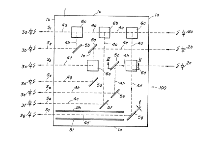
Referring first to Fig. 1, designated at referencenumeral 100 is the entirety of a light-conductive circuit
unit according to a first embodiment of the present inven-
tionD The circuit unit 100 comprises a light-conductive
member 1 made of an optical material, which member 1 is
adapted to serve as a base plate of the unit 100, that is,
as a substrate thereof, while it has a flat square form of
an even thickness. In this embodiment, the light conductive
~0 member 1 has at the right side thereof in Fig~ 1 a side face
la as a surface adapted to receive to let in rays of light,
and at the left side thereof a side face lb as a surface
adapted to let out to project rays of light. In this
respect, the member 1 may have either a top side face lc or
a bottom side face ld thereof let to serve as a light inlet
surface, while letting voluntary one of remaining three side
faces thereof to be a light outlet surface.
_ 5 _
'
~7~3~6
The optical material constituting the light-conductive
member 1 is an acrylic resin having a n~ture of admitting an
incomming beam of light to straightly advance into the
resin, whereas it may be another material such as a polycar-
S bonate resin having a similar light-transmitting nature.
At the right of the light-conductive member 1, in oppo-
sition to the light inlet surface la, there are disposed a
plurality of (three in this embodiment) light-emitting ele-
ments 2a, 2b, 2c composed of light-emitting diodes, the ele-
ments 2a to 2c respectively emitting rays of light which arearranged through a collimator lens (not shown) into paralled
beams penetrating into the light-conductive member 1, at an
incident angle of zero degree, that is, at right angles with
respect to the light inlet surface la.
On the other hand, at the left of the light-conductive
member 1, in opposition to the light outlet surface lb,
there are disposed a plurality o~ (seven in this embodiment)
light receiving elements 3a to 3g composed of photo diodes.
In Fig. 1, represented by broken lines with arrows bet-
ween the light-emitting elements;2a to 2c and the light-
receiving elements 3a to 3g are respective courses as light-
conductive paths 4a to 4h of the beams of light. In this
respect, the light~emitting elements 2a to 2c are spaced
apart from the liyht inlet surface la and hence intercon-
; 25 nected therewith through optical fibers (not shown), as well
as between the light outlet surface lb and the light-
receiving elements 3a to 3g.
- 6 -
.
: .
, ~ -:.. .
7~3~
There will be described below the inner structure of
the llght-conductive circuit unit 100 itself.
In Fig. 1, designated at reference characters 5a to 5g
are slits of a predetermined width 1, respectively; and 6a
to 6e are optical switching elements, respectively. The
slits 5a to 5g are formed, at various points in the way of
the light bea~s, through the light-conductive member 1, as
air gaps extending in the thickness direction of the member
1, respectively, and arranged to be inclined at an angle of
45 with respect to corresponding ones of the courses of the
light beam, so that those courses of the light beams are
reflected at 45 by corresponding ones of the slits Sa to
5g, thus being thereby deflected by 90. In other words,
the slits 5a to 5g are adapted to serve as an optical
deflector, respectively.
Such function of optical deflection of the slits 5a to
5g is derived from the fact that, due to the optical
material of the light-con~uctive member 1 having a suf-
~ ficiently larger index of refraction than air, there is
: 20 occurring a total reflection of light (beam) at the boundary
of the air gap, exemplarily at a boundary surface le of the
light-conductive member 1 defining the slit 5a. In this
. respect, within a range of incident angle capable of causing
such total reflection, the inclination angle of each of the
slits 5a to 5g may be voluntarily deviated from 45 relative
to corresponding one of the courses of light beam, to
thereby deflect to bend this course of light beam by a
. - 7 -
. ':
, . .
3L27Q3gG
desired angle other than 90. Moreover, instead of the
slits 5a to 5g formed as air yap in the light-conductive
member 1, the member 1 may have as many reflection plates as
them each respectively adapted to serve as an optical
deflector. Or otherwise, the slits Sa to 5g may preferably
ha~e silver film deposited on the reflection surfaces
thereof, to thereby assure effective achievement of inten-
sified reflectivity.
As shown in Figs. 2A and 2B, each of ths optical
switching elements 6a to 6e, exemplarily the element 6d in
these Figures, comprises a prism member 8 fitted in a rec-
tangular through-hole 7 formed in the light-conductive
member 1, the prism member 8 having a leter described unique
form stepped along a plane parallel with the light-
~ 15 conductive member 1. It is here advised that the optical
:`:
; switching elements 6a to 6e schematically shown in Fig. 1 is
represented by the element 6d having a side view thereof
shown in Figs. 2A and 2B, and the prism member 8 therer~f as
viewed from a perspective visual point is given in Fig. 3.
The prism member 8, fitted in the through-hole 7 as
described, has fixed thereto, on the top and the bottom, an
~- upper and a lower plate members 9~, 10 adapted to serve as a
flange, respectively. Between the upper plate member 9 and
the upside of the light-conductive member 1 is interposed a
compressed coil spring 11 for normally urging the plate
member 9 together with the prism member 8 in the upward
direction in Fig. 2A. On the other hand, the plate member 9
- - 8 -
, ~
~Q3~3!6
has fixed thereon a downwardly operable push member 12 with
an upward projection 12a functioning as an actuating part of
a pushbutton control of the switching element 6d.
As shown in Fig. 3, the form of the prism member 8 i5
of a rectangular parallelepiped as partially cut to be
stepped to have an upper part 8a of a right-angled triangu-
lar prismal form and a lower part 8b of a quadrangular
prismal form. Incidentally, the prism member 8 shown in
Figs. 2A and 2B is of a side view thereof seen from the
direction X in Fig. 3.
With respect to the prism member 8 shown in Fig. 3,
when normally let into one rectangular side face of ~he
right-angled triangular prismal form of the upper part 8a,
the beam of light as transmitted from the light-emitting
element 2c has a course thereof deflected by 90, on an
oblique side face 8c of the triangular plasmal form, to be
let out from another rectangular side face 8e thereof in a
.
normal direction A, that is, toward the slit 5g in FigO 1.
When normally let into a corresponding side face of the
quadrangular prismaL form of the lower part 8b~ ~he light
beam from the light-emitting element 2c is straightly
transmitted~ as it advances, without deflections of the
course, and let out from an opposite side face 8d of the
quadrangular prismal form in a normal direction B, that is,
~oward the slit 5c in Fig. 1. In other words, in the prism
; member 8, the upper part 8a has a function of deflecting the
course of beam light, and the lower part 8b has a function
:`
_ g _
~` "`' ' ' :
~7~3~t~
of letting the light beam to straight-linearly advance.
More particularly, when the optical switching element
6d is put in a position thereof shown in Fig. 2A and hence
the lower part 8b thereof is positioned to be just fitted in
the through-hole 7 of the light-conductive member 1, then
the beam of light from the light-emitting element 2c is let
to straightly advance; on the other hand, when the upper
part 8a is pushed down to be set in the hole 7, the light
beam is deflected to be bent at a right angle. Accordingly,
with or without pushbutton operation of the switching ele-
ment 6d, the course of the llght beam from the light--
emitting element 2c is selectively determined to be ln the
direction B or A in Fig. 3, that is, to be selectively con-
nected to such one 4h or 4d among the light-conductive paths
4a to 4h that leads to the slit Sc or 5g, respectively. As
a result, the optical switching element 6d is adapted to
serve as a switching means of light transmission route.
Such function of the element 6d is analogous to all of the
remaining optical switching elements 6a to 6c and 6e,
whereas, in the case of the element 6e, the prism member 8
is applied in such a manner that one side face thereof
corresponding~to the side face 8e in Fig. 3 constitutes a
light inlet surface.
.
In the foregoing arrangement, the light~conductive cir-
cuit unit 100 has built thererin, for each of the optical
switching elements 6a to 6e, a holding member (not shown)
adapted to selectively hold the element in position as shown
;;::
-- 10 --
;
:,..
}
'
~7~3~1i
in Figs. 2A and 2s.
Moreover, besides the upper part 8a as a light
transmission route turning portion and the lower part 8b as
a light transmission route straight-forwarding portion, the
prism member 8 may preferably have another part adapted to
interrupt the transmission of light or cut off a light
transmission route. According to such modification, there
is achieved a p~ism member permitted to exhibit three dif-
ferent functions: turing, straight-forwardingt and cut-off
of the light transmission route. As a result, such as when
exemplarily the switching element 6b as modified as
described above is employed as a control switch of a fan for
a passenger room, there can be achieved a three-staged
switching control with an off, a mild, and a strong control
positions.
In the light-conductive circuit unit 100, the light-
conductive paths 4a to 4h have circuit patterns thereof
dètermined depending on the arrangement of the optical
switcing elements 6a to 6e as ~ell as of the slits Sa to Sg,
while the circuit patterns, which are each respectively
defined as a part of the light-conductive member l itself,
are~invisible, though actually present.
As shown in Fig. 1, the three beams of light as pro-
jected from the light-emitting elements 2a to 2c and
received through the li~ht inlet surface la are transmitted
through the light-conductive paths 4a to 4h and let out, at
the light outlet surface lb, as a set of seven optical
-- 11 -
~ ,
,3~i
signals Sl to S7 to be input to the light-receiving elements
3a to 3g, the optical signals Sl to S7 having alternatively
selectable "on" and "off" signal states, respectively.
For example, while the switching elements 6a and 6b are
set in beam direction holding positions thereof, the optical
signals Sl to S7 have such signal states as described below.
The light beam ~rom the light-emitting element 2a is
admitted to straight-linearly pass the switching elements
6a, 6b, thus leading to the switching element 6c, while it
is kept from advancing along the paths 4c, 4d, so that the
signal S6 is kept "off". Additionally, when the switch ele-
ment 6c is operated into a beam direction turning position
thereof, the signal Sl becomes "off" and the signal S2
beomes "on", whereas, while the element 6c is set in a beam
direction holding position thereof, the signals Sl, S2 are
in "on" and "off" states, respectively. The states of the
signals S3, S4 and those of the signal S5t S7 depend on the
switch position of the switching element 6e and that of the
switching element 6d, respectively.
Incidentally, the light-conductive paths 4a to 4h are
; patterned to be parallel with and/or perpendicular to each; other; exemplarily, the path 4g is parallel with the path
4h, and the path 4e is perpendicular to the path 4d. Any
two light-conductive paths nelghboring or crossing each
other are designed to be free from optical interference
therebetween. In this respect, to fu,rther ensure non-
interference with light in the path, as well as for the pro-
.
- 12 -
, .
' ' :
' :
. - :
~7~3~6
tection against optical disturbances from outside, a relati-
vely long path portion 4d'is provided therealong with a pair
of guide slits Sh, 5i formed, at the transversely inner and
outer sides thereof, to be cut through in the thickness
direction of the light-conductive member l.
According to the present embodiment, the light-
conductive circuit unit lO0 comprises the single light-
conductive member l which has a desiyned light-conductive
circuit substantiated inherently by no more than forming at
necessary points the respective slits 5a to 5g as well as
holes 7 to be fitted with the optical switching elements 6a
to 6e, thus permitting an optical circuit, even of a compli-
cated pattern, to be constituted with great ease. Moreover,
the light-conductive member 1, as a single body capable of
moulding with a form, is easy to manufacture and favorably
adapted for mass production. Particularly, with the pre-
sence of the inherently required fitting holes 7 for the
switching elements 6a to 6e, the member l to be mounded as a
unit base is able to achieve simplification as well as faci-
litation in the assembly work of the light-conductive cir-
cuit unit 100.
Further, in the light-conductive circuit unit lO0, ~
necessary circuit elements thereof including the switching
elements 6a to 6e and the slits Sa to 5g are formed to be
substantially integral with the unit base l constituting the
light-conductive paths 4a to 4h, thus effectively preventing
the light leakage which otherwise would occur at connecting
- 13 -
', .
~. :.. ~. ;. ..
~Z76P3~36
points between such circuit components, so that a sufficient
transmitting efficiency of light can be secured of the
light-conductive circuit unit 100 itself as well as of the
entirety of an optical signal transmission system having
S employed the circuit unit 100.
Incidentally, in a modified example of the foregoing
embodiment, exemplarily the light-emitting element 2c may be
constituted as a light source adapted to emit rays of light
having a plurality of different wavelengths. In such modi-
fication, the optical switching element 6a may preferably
have inlaid, in the lower part 8b of the prism member 8, a
reflection plate adapted to reflect no more than those rays
of light in a light beam transmitted thereto whlch have a
certain predetermined wavelength, the reflection plate being
inclined at an angle of 45 with respect to the course of
the light beam, to thereby deflect or turn by 90 the rays
- of light of the predetermined wavelength. According to such
. - .
modification, the light-conductive circuit unit 100 may be
:~ , .
advantageously adapted for a multiplex optical signal
transmission system of a multi-wavelength type.
There will be described hereinbelow a second embodiment
of the present invention, with reference to Fig. 4 which is
a side view of a light-conductive circuit unit 200 according
to this embodiment.
~,.
Different from the first embodiment in which the light-
conductive member 1 is of a flat plate form as a whole, the
~,
second embodiment provides a light-conductive member 201 of
~,
- 14 -
l ,~
3~6
a three-dimensional figure formed to be channel-like in the
side view with three flat portions 210a, 201b, 210c dif-
ferent in the level from each other. The respective flat
portions 201a to 201c have light course switching means
thereof consisting of optical switching elements 206 and a
plurality of slits (not shown), the switching elements 206
as well as the slits being of such a type that is analogous
to the type described in the first embodiment. Among the
flat portions 201a to 201c, upper two 201a, 201c extending
at higher levels than the remaining one 201b are intercon-
nected with the latter 201b through a pair of vertically
standing portions 201d for the conduction of light therebet-
ween, respectively. With such structure, the circuit unit
200 is advantageously permitted to have an optical circuit
lS thereof scaled up, therehy achieving increased flexibillty
in the selection for lay-out of operating means of the
switching elements 206 to be adequately located in accor-
dance~with available space for the installation of the unit
; 200
As will be understood from the foregoing description,
;according to the present invention, an optical circuit to be
used in an optical signal processling system is integrally
constituted as a unit comprising a single light-conductive
member having a plurality of re~lection parts as well as a
plurality of optical switching elements, thereby achieving
facilitation in the manufacture of complicated optical cir-
cuits to be made compact, while permitting like optical cir-
- 15 -
, . ,.. ~ , ~ , "
~;~7~3~i
cuits to be mass-produced with like characteristics~
Moreover, possible integration of associated light-
conductive paths into a single member allows the number of
optical connections therebetween to be minimised, thereby
raising the light transmission efficiency of optical cir-
cuit.
Further, it also will be comprehended from the
foregoing description of the first and the second embodi-
: ments that, according to the present invention, there is
provided a light-conductive circuit unit compris~ing, when
most simplified in the constitution, besides necessary
: light-conductive paths, (i) an arrangement having, for a
single light source, a single optical switching element and
a single light course turning slit or (ii) an arrangement
lS having a pair of optical switching elements each respec-
tively provided for one of a pair of light sources.
~: Exemplarily, the former (i) corresponds to an arrangement
,, .
. :.including, for the light-emitting~element 2a, the switching
element 6c:and the slit~Sb (cooperating with each other to
~: 20 supply the optical signals Slj S2 to the light-receiving
elements 3a, 3b); and the latter (ii), to an arrangement
including the switching elements 6c, 6d provided for the
. light-emitting elements 2a, 2c, respectively, (to supply the
optical signals Sl, S5 to the light-receiving elements 3a,
3e, such that the light beam from the light-emitting element
2c is let to straight-linearly advance to reach the light-
~ receiving element 3e when the switching element 6d is set in
:~:
- 16 -
. ~
', : ' ' '
~Z7~3~
the light course holding position, on the assumption that
the slits 5c; 5e, which are redundant in such arrangement,
was eliminated and hence the beam of light of the signal S5
and the element 3e ~ere put in place of that o~ the signal
S3 and the element 3c, respectively).
Still more, the configuration itself of the light-
conductive member 1 or 201 as a unit base, that i5, as a
substrate of circuit unit is not limited to the flat plate
or channel-like form, but may have a voluntary form as prac-
ticable.
Although there have been described what are at presentconsidered to be the preferred embodiments of the invention,
it will be understood that the present invention may be
embodied in other specific forms without departing from the
spirit or essential characteristics thereof. The present
embodiments are therefore to be considered in all respects
:.:
as illustrative,and not restrective. The scope oE the
invention is indicated by the appended claims rather than by
the foregoing description.
::