Note: Descriptions are shown in the official language in which they were submitted.
~7~5~
COLOR TEMPERATURE AUTOMATIC ADJUSTING SYSTEM
BACKGROUND OF THE INVENTION
_ _ .
Technical Field of the Invention
The presen-t invention relates generally to a color
temperature automa-tic adjusting system for a color
television receiver. More specifically, the invention
relates to an automatic white balance adjusting system
which can eliminate unstable pictures in the transition
period after turning on the power switch of the color
television receiver.
Background Art
Television receivers contain automa-tic white balance
circuits of the type disclosed in published European
Patent Application No. 0 192 413. Such circuits monitor the
cathode beam currents for the cathode ray tube and
adjust the gains of the primary color signal circuits
accordingly to maintain a white balance.
A problem arises, however, when the television
receivers are first switched on. Since the heater for
the cathode electrode of the display tube is cold when
the television receiver is turned on, -the primary color
signal circuits are controlled so as to be in a
condition to cause the cathode beam currents to flow at
a maximum value. Thus, when the heater is heated
sufficien-tly, and the cathode emission begins, the
video screen becomes too bri~ht during a transien-t time
until the ~uto white balance circuit becomes
stabilized. Also, since the cut-off voltage EKCO of
the display tube is scattered between the red color,
the ~reen color and the blue color cathodes, the auto
white balance circuit will be stabilized after
~7~55i~
PATENT
2--
different times for red, green and blue, and the color
of the picture will fluctuate.
The Japanese Patent First Publication (Tokkai)
Showa 55-67286 discloses a white balance adjusting
apparatus which attempts to overcome this problem. In
the disclosed system, the automatic control loop is
cutoff and a white balance adjusting voltage is
supplied from a predetermined bias source upon turning
on the power supply for a television receiver. The
cutoff condition of the automatic control loop is
maintained for a predetermined period of time after
turning on the power supply. Upon expiration of the
predetermined period, the power supply for the
automatic adjusting loop is resumed. Therefore, the
automatic adjusting loop becomes operative after a
given delay time corresponding to the aforementioned
predetermined period after turning on the power supplyO
Then, automatic white balance adjustment takes place by
means of the automatic control loop.
However, since the picture is immediately
displayed in response to turning on the power supply
for the television receiver, an unadjusted picture
becomes visible while the automatic adjusting loop i5
held inGperative. Furthermore, even after resumption
of the operation of the automatic control loop, the
picture condition becomes unstable during the
transition period while the white balance adjustment
takes place. Therefore, in the system disclosed in the
Tokkai Showa 55-67286, it is inevitable that an
unstable picture condition occurs during the turn on
transition period.
~27 135~
PATENT
--3--
DISCLOSU~E OF THE INVENTION
Therefore, it i5 an object of the present
invention to provide an automatic color temperature
adjusting system which can eliminate the unstable
picture condition during the turn on transition period.
In order to accomplish the aforementioned and
other objects, an automatic color temperature adjusting
system, according to the present invention, is
comprised of a gain control circuit associated with a
feedback loop for controlling the gain characteristics
of an amplifier in each color channel. The gain
control circuit, in response to the turning on of the
power supply, lowers the gain at each amplifier to a
given level. The gain control circuit adjusts the gain
at each amplifier to gradually increase the gain to
reach a normal gain level after a given period of time~
In practice, the given period of time during which
it is necessary to maintain the gain of each amplifier
at a lower than normal level is chosen to be long
enough to sufficiently heat the color picture tube
cathode of the color channel associated with that
amplifier for normalizing cathode emission. During
this turn on transition period, the gain at each
amplifier is increased corresponding to the increase in
emission of the corresponcling cathode. As a result,
the unstable picture condition during the turn on
transition becomes invisible so that there is a smooth
transition to a stable picture display.
According to one aspect of the invention, an
automatic color temperature adjusting system for a
color television receiver having a color picture tube
which includes a plurality of cathodes to be
respectively driven by different corresponding color
channel primary color signals, comprises means,
`` ~ 5~i~
PATENT
--4--
including a plurality of primary color signal channels,
for supplying respective channels of primary color
signals to the corresponding cathodes in the picture
tube, means, disposed in each of the primary color
signal channels, for amplifying the corresponding
channel of the primary color signal at a controlled
level, and means for feedback controlling the
amplifying characteristics of each amplifying means so
as to adjust the cathode beam current of the white
level at an optimal level, the feedback controlling
means being responsive to a turning on of the power
supply to adjust the amplifying characteristics of the
amplifying means to set the cathode beam current at a
predetermined minimum level and subsequently, gradually
increasing the cathode beam current to a normal level
in a given period of time.
In the practical construction, the gain of the
amplifying means is variable inversely with respect to
a control voltage applied thereto from the feedback
controlling means, and the feedback control means
includes a transition control signal generator which is
active during the turn on transition period for
initially setting the control voltage at a
predetermined maximum level and gradually decreasing
the level toward a normal level within the turn on
transition period.
The feedback control means adjusts the gain of the
amplifying means to increase the cathode beam current
according to the increase in emissions of the cathode.
In order to adjust the gain of the amplifying means, it
is preferred to construct the feedback controlling
means to include an error signal generator means for
comparing a voltage representative of the cathode beam
current with a predetermined reference voltage to
S~i6
PATENT
derive a difference therebetween and producing an errox
signal indicative of the difference. The feedback
controlling means may further comprise a sample and
hold circuit to sample and hold the error signal to
produce the control voltage based on the held error
signal level. The sample and hold circuit operates
during a white level blanking period to sample the
error signals and holds the error signal level to
output a constant control voltage upon termination of
the white level blanking period.
In practice, the automatic color temperature
adjusting system further comprises means, active during
the white level blanking period, for adding a
predetermined white level reference signal to the
corresponding channel of the primary color signal.
According to one embodiment, the transition
control signal generator is associated with the sample
and hold circuit to supply a transition control signal
in order to initially raise the output of the sample
and hold circuit to a maximum level in response to the
turn on of the power supply and, subsequently,
gradually decrease the level of the transition control
signal to decrease the output level toward the normal
level within the turn on transition perlod. In an
alternative embodiment, the transition control signal
generator is associated with the error signal generator
means to supply a transition control signal to the
latter for adjusting the input voltage signal to a
maximum level in response to the turning on of the
power supply and, subsequently, gradually decrease the
input level toward the normal level within the turn on
transition period. Furthermore, the transition control
signal generator includes a time constant circuit which
provides a predetermined delay time for lowering the
~;~7~55~;
PATENT
-6-
signal level o the transition control signal to a zero
level after turning off of the power supply so that the
transition control signal will resume at the level
existing when the power was turned off.
BRIEF DESCRIPTION OF THE DRAWINGS
The present invention will be understood more
fully from the detailed description given hereinafter
and from the accompanying drawings of the preferred
embodiment of the invention, which, however, should not
be taken to limit the invention to the specific
embodiment but are for explanation and understanding
only.
In the drawings:
Fig. 1 is a block diagram of the prefe,rred
embodiment of an automatic color temperature adjusting
system according to the invention;
Fig. 2 is a block diagram of a white level
adjusting feedback system in the preferred embodiment
of the automatic color temperature adjusting system of
Fig. l;
Fig. 3 is a chart showing the timing of the
blanking period, in which color temperature adjustment
is performed, in relation to the color video signal;
Figs. 4(A) and 4(B) are charts showing variations
of the transition control voltage, the voltage
corresponding to the cathode beam current and the gain
of the voltage controlled amplifier employed in the
preferred embodiment of the automatic color temperature
adjusting system;
Fig. 5 is graph showing variations of the cathode
beam current and the cathode emission;
Fig. 6 is a chart showing the variation of the
transition control voltage to be produced in the
~L~7~
PATENT
--7--
preferred embodiment of the automatic color temperature
adjusting system when the power supply is switched on,
off and on again within a short period; and
Fig. 7 is a block diagram similar to Fig. 2 but
showing another embodiment of the automatic color
temperature adjusting system according to the
invention.
BEST MODE FOR CARRYING OUT THE INVENTION
Referring now to the drawings, particularly to
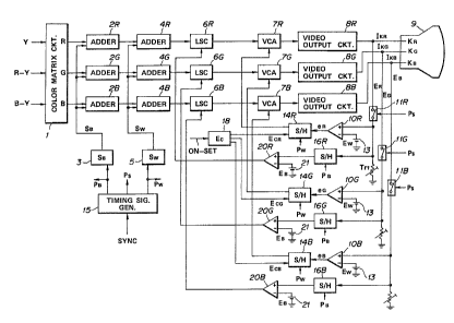
Fig. 1, the preferred embodiment of an automatic color
temperature adjusting system, according to the
invention, is provided in a color television circuit
which has a color matrix circuit 1. The color matrix
circuit 1 is connected to a composite video signal
source (not shown). As is well known, the typical
composite video signal source comprises a television
tuner circuit, a video detector, a luminance
signal/chrominance signal separator circuit, a
luminance amplifier and a color demodulator, for
example. The tuner circuit receives a video signal
through an antenna input terminal, ~or example. The
video detector circuit receives an amplified
intermediate frequency si.gnal from the tuner circuit to
output the composite video signal. The luminance
signal/chrominance signal separator circuit separates
luminance signal Y and the chrominance signal~ The
lumi.nance signal output from the luminance
signal/chrominance signal separator circuit is fed to
the color matrix circuit 1 through a luminance
amplifier. The chrominance signal is input to the
color demodulator circuit. The color demodulator
circuit produces a red color difference signal R-Y and
a blue color difference signal B-Y based on the input
7~ ii6
PATENT
--8--
chrominance signal. These color difference signals R-Y
and B-Y are also input to the color matrix circuit 1.
The color matrix circuit 1 performs a matrix resolution
of the luminance signal Y and the color difference
signals R-Y and B-Y to produce red, green and blue
primary color signals R,G and B.
The red, green and blue primary color signals R, G
and B are supplied to adders 2R,2G and 2B,
respectively. The adders 2R,2G and 2B are connected
to a black level reference signal generator circuit 3
which produces a black level reference signal SB. The
adders 2R,2G and 2B add the black level reference
signal SB to respective red, green and blue primary
color signals R,G and B. The outputs of the adders
2R,2G and 2B are fed to adders 4R,4G and 4B,
respectively, which are, in turn, connected to a white
level reference signal generator 5. The white level
reference signal generator 5 produces a white level
reference signal Sw. The adders 4R,4G and 4B add the
white level reference signal Sw to the respective
inputs from the associated adders 2R,2G and 2B.
The outputs of the adders 4R,4G and 4B are input,
respectively, to level shifter circuits 6R,6G and 6B.
The level shifter circuits 6R,6G and 6B are active
during the blanking period at a controlled timing. The
level shifter clrcuits 6R,6G and 6B have variable
gains to adjust the beam current of the black level.
The outputs of the level shifter circuits 6R,6G and 6B
are input to voltage controlled amplifiers 7R,7G and
7B, respectively, which also have variable gains. The
voltage controlled amplifiers 7R,7G and 7B are
connected to video output circuits 8R,8G and 8B,
respectively, which include amplifiers. The video
output circuits 8R,8G and 8B are connected,
12~
P~TENT
_g_
respectively, to an associated red cathode KR, an
associated green cathode KG and an associated blue
cathode KB f color picture tube 9. The video output
circuits 8R, 8G and 8B generate variable cathode beam
currents IKR, IKG and IKB, respectively, to be applied
to the associated cathodes KR, KG and KB, respectively,
depending upon the gains at the voltage controlled
amplifiers 7R, 7G and 7B, respectively.
The video output circuits 8R, 8G and 8B are also
connected to one input terminal of differential
amplifiers lOR, lOG and lOB, respectively, and sample
and hold circuits 16R, 16G and 16B, respectively, via
switching circuits llR, llG and llB, respectively. The
switch circuits llR, llG and llB are connected to a
timing signal generator circuit 15 to receive therefrom
a sampling pulse Ps to cause voltage signals ER, EG and
EB, having voltages respectively corresponding to the
current values of the cathode beam currents IKR, IKG
and IKB, to be supplied to the inputs of the respective
amplifiers lOR, lOG, and lOB while the sampling pulse
is present. The timing signal generator circuit 15
generates the sampling pulse at a controlled timing
which is derived on the basis of the synchronization
signals.
The other inputs of the. operational amplifiers
lOR, lOB and lOC are connected to a reference voltage
source 13 to receive therefrom a reference voltage Ew.
The operational amplifiers lOR, lOG and lOB produce
error signals eR, eG and eB, respectively. The error
- signals eR, eG and eB are fed to the sample and hold
circuits 14R, 14G and 14B, respectively. The sample
and hold circuits 14R, 14G and 14B are connected to the
timing signal generator 15 to receive therefrom
sampling pulses Pw. Namely, the sample and hold
s~
PATENT
--10--
circuits 14R, 14G and 14B sample the error signals eR,
eG and eB, respectively, in response to the sampling
pulse Pw from the timing signal generator 15 and hold
the error signal values while the sampling pulses are
absent.
The sample and hold operations of the sample and
hold circuits 16R, 16G and 16B are controlled by a
sampling pulse PB input from the timing signal
generator 15. Namely, the sample and hold circuits
16R, 16G and 16B sample the values of the voltage
signals ER, EG and EB, respectively, which are
indicative of the current values of the beam currents
IXR~ IKG and IXB~ respectively, in response to the
sampling pulses PB from the timing signal yenerator 15
and hold the sampled beam current values while the
sampliny pulses Pw are absent.
The sample and hold circuits 14R, 14G and 14B are
connected to the voltage controlled amplifiers 7R, 7G
and 7B, respectively, to feed them the control voltages
ECR~ ECG and ECB indicative of the held error signal
values eR, eG and eB, respectively. A transition
control voltage generator 18, in response to the
turning on of the power supply to the television
receiver, outputs separate initial control voltages
EcR, ECG and ECB which are added to the outputs of the
sample and hold circuits 14~, 14G and 14B,
respectively, and the sums are supplied to the voltage
controlled amplifiers 7R, 7G and 7B, respectively, as
will be explained in greater detail further in this
description. The gain of the voltage controlled
amplifiers are varied in the opposite direction of the
variation of the control voltage signals supplied
thereto. These voltage signals ECR~ ECG and ECB are
PATENT
--11--
inversely indicative of the cathode heam current levels
to be held during turn on.
As will be appreciated, the voltage controlled
amplifiers 7R, 7G and 7G, the video output circuits ~R,
8G and 8B, the operational amplifiers lOR, lOG and lOB
and the sample and hold circuits 14R, 14G and 14B form
feedback loops for controlling the gain of the voltaye
controlled amplifiers.
The sample and hold circuits 16R, 16G and 16B
sample the voltages of the voltage signals ER, EG and
EB, respectively, in response to the sampling pulse PB
from the timing signal generator 15. The sample and
hold circuits 16R, 16G and 16B hold the voltaye signal
values ER, EG and EB, respectively, and output the held
values to respectively associated operational
amplifiers 20R, 20G and 20B. The operational
amplifiers 20R, 20G and 20B also receive a reference
voltage EB from a reference voltage source 21. The
operational amplifiers 20R, 20G and 20B produce error
signals representative of the differences between the
voltage signal values ER, EG and EB, respectively, and
the reference voltage EB. The error signals produced
by the operational amplifiers 20R, 20G and 20B serve as
control voltages for the black level setting circuits
6R, 6G and 6B, respectively, for controlling the gain
thereof.
The timing signal generator 15 is connected to the
black level reference signal generator circuit 3, the
white level reference signal generator circuit 5, and
the sample and hold circuits 14R, 14G, 14B and 16R,
16G, 16B for supplying the timing pulses Pw and PB. In
order to produce the timing pulses Pw and PB, the
timing signal generator 15 receives synchronization
signals, i.e., vertical synchronization signals and
` ~ ~7~5~i Eii
PATENT
-12-
horizontal synchronization siynals. The timing pulse
generator 15 is responsive to the vertical
synchronization signal reproduced at the end of the
vertical blanking period to produce the timing signal
PW for one horizontal scanning period. For the next
one horizontal scanning period, the timing signal PB is
produced by the timing signal generator 15.
The aforementioned circuit performs white balance
adjustment by adjusting the gain of the voltage
controlled amplifiers 7R, 7G and 7B at the timing
controlled by the timing signals Pw and PB. The
details of the gain control system for the voltage
controlled amplifiers 7R, 7G and 7B and the operation
thereof will now be described with reference to Figs. 2
to 6.
It should be appreciated that, since the feedback
systems for control.ling the gains of the vol-tage
controlled amplifiers 7R/ 7G and 7B are of identical
construction, the detailed circuit construction of only
the red channel feedback system is illustrated in Fig.
2.
As seen from Fig. 2, the video output circuit 8R
- includes an npn-type transistor Q1 The base electrode
of the transistor Q1 is connected to the output of the
voltage controlled amplifier 7R to receive the red
channel primary color signal R from the voltage
controlled amplifier 7R. The emitter electrode of the
transistor Ql is grounded via a resistor RE. The
collector electrode of khe transistor Q1 is connected
to a power supply terminal +B via a resistor RL. The
collector electrode of the npn-type transistor Q1 is
also connected to the base electrode of a pnp-type
transistor Q2. The emitter electrode of the transistor
Q2 is connected to the cathode KR that provides the red
i56
PATENT
-13-
color gun of the color picture tube 9. The collector
electrode of the transistor Q2 is connected to the
circuit ground via a series circuit comprised of a
diode D, the pnp-type switching transistor Q3 (which
constitutes the switch llR), and a variable resistor
Trl ~
The control voltaye generator 18 comprises a time
constant circuit 30 constituted by a capacitor C
connected in series with a resistor Rl between the
power supply terminal +B and the circuit ground, an
npn-type transistor Q4, and diodes Dl, D2 and D3. The
transistor Q~ employed in the shown embodiment
constitutes an emitter follower. The base electrode of
the transistor Q4 is connected to the junction of the
capacitor C and the resistor Rl. The cathode
electrodes of the diodes Dl, D2 and D3 are respectively
connected to the sample and hold circuits 14R, 14G and
14B. The anodes of the diodes Dl, D2 and D3 are
connected to the emitter electrode of the transistor
Q4-
As shown in Fig. 2, each sample and hold circuit14R, 14G and 14B comprises an on/off switch 31 whose
switch contact position is controlled by the timing
signal Pw f the timing signal generator circuit 15,
which serves as the sampling pulse. Each of the sample
and hold circuits 14R, 14G and 14B further comprises a
capacitor Cs to be charged by the error signal output
from the associated operational amplifier lOR, lOG and
lOB. In the example of Fig. 2, the switch 31 is turned
on in response to the timing pulse Pw and held at the
on position for the period while the timing pulse PW is
held at the HIGH level. During this period, the
capacitor Cs is charged by the error signal eR from the
operational amplifier lOR. When the timing pulse Pw
~2~ iS6
PAT~ENT
-14-
changes to a LOW level, the switch 31 is opened to
disconnect the capacitor Cs from the operational
amplifier 10R. Therefore, the error signal eR charged
to the capacitor Cs during the period of the timing
pulse Pw is supplied to the voltage controlled
amplifier 7R until the next timing pulse Pw turns on
the switch 31.
In the preferred construction, a discharge circuit
32, including a diode Do in series with a resistor R2,
may be connected in parallel with the resistor R1 in
the transition control voltage generator circuit 18, as
illustrated by the phantom line in Fig. 2. In this
case, the resistance of the resistor R2 may be selected
in relation to the capacity of the capacitor C so that
the discharge characteristics of the discharge circuit
may approximately correspond to the heat discharging
characteristics of the cathode KR.
In the circuit arrangement as set forth above, the
cathodes KR, KG and KB f the picture tube 9 are driven
by the red, green and blue primary color signals R, G
and B, respectively, to display color picture on the
video screen of the picture tube in the usual fashion.
The customary deflection circuits are not shown since
they form no part of the invention.
Referring again to Fig. 1, the timing signal
generator 15 receives the vertical and horizontal
synchronization signals to produce horizontal blanking
pulses, after a vertical blanking period of 5 to 6
horizontal scanning periods. As shown in Fig. 3, the
horizontal blanking pulses generated by the timing
signal generator 15 serve as respective timing pulses
PW and PB. Namely, throughout the first horizontal
scanning period immediately after termination of the
vertical blanking period, the timing pulse Pw is
~7~;S~
P~TENT
--15--
produced and maintained at a HIGH level. The timing
pulse PB is produced and maintained at a HIGH level for
the second horizontal scanning period. The timing
pulse Pw is supplied to the white level reference
signal generator circuit 5. Therefore, the white level
reference signal generator circuit 5 becomes active in
the first horizontal scanning period to output the
white level reference signal Sw having a luminance
level in a range of 50-60 IRE. In the second
horizontal scanning period, the timing pulse PB is
supplied to the black level reference signal generator
circuit 3 to activate the latter. The black level
reference signal generator 3 thus becomes active to
output the black level reference signal SB having a
luminance level of 5 IRE.
It should be appreciated that, during the
aforementioned blanking period, the video output
circuits 8R, 8G and 8B are held nonconductive to the
red, green and blue primary color signals R, G and B,
respectively, in a per se well known manner, as for
example, shown in published European Patent Application
No. 0 192 413. Therefore, flyback lines are prevented
from appearing on the video screen.
The timing signal generator 15 also outputs a
timing signal PS which is held at a HIGH level
throughcut the blanking period. The timing siynal Ps
is supplied to the switching circuit llR which
corresponds to the transistor Q3 in Fig. 2. A HIGH
level timiny pulse Ps, causes the switching circuit llR
(as well as the other switches llG and llB) to become
conductive to feed the voltage signals ER, EG and EB,
respectively, to the operational amplifiers lOR, lOG
and lOB, respectively, of the white balance feedback
control systems of the respective color channels, and
PATENT
-16-
to the sample and hold circuits 16R, 16G and 16B,
respectively, of the black level feedback control
systems of respective color channels.
The timing pulse Pg is also supplied to the sample
and hold circuits 16R, 16G and 16B to place them in the
sample mode. While the timing pulse P~ is held at the
HIGH level, the sample and hold circuits 16R, 16G and
16B sample the voltage signals ER, EG and EB,
respectively. The sample and hold circuits 16R, 16G
and 16B, in response to the termination of the HIGH
level timing signal PB, hold the voltage signal values
ER, EG and EB, respectively, and output them as
constant voltage signals. The operational amplifiers
2OR, 2OG and 2OB, respectively, compare these voltage
signals with the reference voltage EB to produce error
signals. The error signals are fed back to the level
shifter circuits 6R, 6G and 6B to adjust the black
level for respective color channel primary color
signals.
As set forth above, since the timing signal PB is
generated during the second horizontal scanning period,
the aforementioned black level adjustment takes place
during the second horizontal scanning period.
The white level adjustment takes place during the
first horizontal scanning period in response to the
timing pulse Pw. In the white level adjustment, the
operational amplifier lOR compares the voltage signal
ER, supplied from the switching transistor Q3, with the
reference voltage Ew to output the error signal eR.
The sample and hold circuit 14R samples the error
signal value eR while the HIGH level timing signal Pw
is supplied. The sample and hold circuit 14R holds the
sampled error signal value eR in response to
termination of the timing signal Pw and outputs a
PATENT
-17-
constant voltaye control signal ECR to the voltage
controlled amplifier 7R. Referring again to Fig. 2,
the operation of the auto white balance circuit during
turn on will now be explained.
When the power supply is turned on at a time to,
the cathode emission KE and the cathode beam current
IKR increase as illustrated in Fig. 5. The capacitor C
is also charged rapidly. As a result, the voltage
applied to the base electrode of the transistor Q4
increases quickly to turn the transistor on.
Immediately after being fully charged, the capacitor C
starts discharging. The discharge voltage of the
capacitor C is supplied through the now conductive
transistor Q4 to the capacitor Cs of the sample and
hold circuit 14R, as the initial control voltage ECR
At this time, the initial control voltage ECR has
momentarily risen to the maximum level, and then
gradually decreases according to the time constant of a
time constant circuit 30 as shown in Fig. 4A. On the
2~ other hand, during the transition which the cathode
emission KE gradually increases, the amplitude of the
error signal according to the increase of the cathode
beam current IKR as shown in Fig. 4A.
While the amplitude of the initial control voltage
ECR is bigger than the amplitude of the error signal
eR, the diode D1 is conductive and so the initial
control voltage ECR is supplied to the voltage
controlled amplifier 7R.
At a time t, as the amplitude of the error signal
eR becomes bigger than the initial control voltage ECR~
the diode D1 becomes non-conductive and then the error
signal eR is supplied to the voltage controlled
amplifier 7R instead of the initial control voltage
EcR.
~27~
PATENT
-18-
Accordingly, the gain Ga of the voltage controlled
amplifier 7R varies in accordance with the control
voltages ECR or eR as shown in Fig. 4B.
As shown in Fig. 6, when the power supplv is
once turned on at a time to~ off at a time t1 after a
substantially short period after the time to, and again
turned on at a time t2 after a substantially short
period from the time tl, the discharge circuit 32 in
the transition control voltage generator 18 serves to
vary the initial control voltage as shown. Namely,
since the discharge circuit 32 has a time constant
determined by the resistance of the resistor R2 and the
capacity of the capacitor C, which substantially
corresponds to the heat discharge characteristics of
the cathode, the capacitor C is held at a charged
condition even after turning off the power supply.
Therefore, when the power supply is again turned on at
the time t2, the discharge of the capacitor C is
resumed from the level existing when the power was
turned off. Therefore, even when the power switch is
operated to turn on, off and on again within a short
period, smooth transition can be provided.
Fig. 7 shows another embodiment of the white
balance adjusting feedback system. In this embodiment,
a transition control circuit 40, similar in
construction to the transition control voltage
generator 18 and therefore supplied with the same
reference numerals, is connected between the switching
transistor Q3 and the operational amplifier lOR. The
transition control circuit 40 is designed to raise the
voltage signal ECR to be applied to the operational
amplifier lOR to the maximum level in response to
turning on the power supply. In a manner similar to
that described above for the transition control voltage
~270~i~i6
ATENT
--19--
generator 18, the transition control circuit 40
operates to gradually decrease the voltage signal level
ECR to the normal level in a predetermined period of
time.
As set forth with respect to the former
embodiment, the voltage of the voltage signal ER
increases as the cathode emission increases and thus as
the cathode beam current increases. When the power is
turned on, the capacitor C immediately charges and the
transistor Q4 turns on to apply the voltage charge on
the capacitor C to the input to the amplifier 10R. As
the capacitor C discharges and the initial control ECR
is decreasing, the voltage ER increases. Therefore,
when the initial control voltage is bigger than the
voltage ER, the initial control voltage is supplied to
the operational amplifier 10R, because the diode Dl is
conducti.veO On the other hand, when the voltage
becomes bigger than the initial control voltage ECR~
the voltage ER is supplied to the operational
amplifier, because the diode Dl is not conductive.
Similarly to the former embodiment, smooth turn on
transition can thereby be provided.
While various switches have been shown and
described in terms of mechanical switches, it will be
understood that in the actual embodiments such switches
are electronic switches.
While the present invention has been disclosed in
terms of the preferred embodiment in order to
facilitate better understanding of the invention, it
should be appreciated that the invention can be
embodiecl in various ways without departing from the
principle of the invention. Therefore, the invention
should be understood to include all possible
embodiments and modifications to the shown embodiments
-20- PATENT
which can be embodied without departiny from the
principles of the invention set out in the appended
claims.