Note: Descriptions are shown in the official language in which they were submitted.
~7~
BACXG~OUND OE THE INVENTION:
This invention relates to an optical memory device
comprising a bistable semiconductor laser, Tne optical memory
device is not only useful as an optical m.emory element but also
in an optical master-slave flip-flop device and in an o?tical
signal shift:!rg device or optical shifL registsr, The o?tioal
.rnemort e].eme~ts, the optical n.aster-sl2~rs flip-flop dev~ce, _nl
the o?tical s~nal shiftir.~ device a.~_ useful in an o?t ~ 7i~al
computer,
1~ A semiconductor laser having a bistabi'ity, is rev_alsd
in a letter contribut~d by H, Xawagllchi to Elsctronics Letters,
Vol, 17, Mo, 20 (lst O^tober 1981), pages 741 and 742, under
the title of "Bistable Operation of' SeMiconductor Lasers by Optical
Injection," It is possi'ole to manufacture an optical memory
device by using the bistable semiconductor laser in the manner
which will later oe described a li.ttle More in detail, The optical
memory device is, however, not satisfactorily operable when two
optical input si~nals are simultaneously supplied thereto,
An improved bistable semiconductor laser is disclosed
23 and used in an optical memory device in a report which is read
by Y, Odagiri and K, Komatsu at Conference on Lasers and Electro-optics
held ~une 19-22, 1984, and is printed in Technical l)igest of the
.. ' ~
~7~
conference, ?ages 184 throu~h 186, undsr the title of "Bistable
Laser-diode Memory for 3ptical Tlme-division Switching Applications"
(Report No.THJ3)~ The Odagiri et al report, however, does not
teach selective memory of two optical input signals which are
concurrently supplied to the optical memory device,
It is possible by using a pair of optical memory devices,
each comprising the im?roved bista'ole semiconductor laser, to
manufacture an optical master-slave flip-flop device, The flip-flop
device must, however, comprise an optical isolator between the
optical memory pair as will later be pointed out more in detail,
T'ne optical isolator cor.plicates the circuitry and renders it
difficult to implement the fli?-flop device as an integrated
circuit,
To s?e~:~ of electrical sig.r.zls, logic o?eration is
carried out at a hi~h speed by a high-spead logic o?eration device
which ~,ay comprise Joshephson junction devicas, Optical signals
are often used in rspre3enting two-dimensional digital information
of a large quantity, Conversion of the optical signals to electrical
signals on carrying out logic operation, is oojectionable in
view of the speed of operation and the power consumption, It
is therefore disiraole to provide a satisfactorily operable optical
memory device in order to carry out the logic o?eration ~lirectly
on the optical signals,
SU~I~ARY OF THE INVENTION:
It is therefore an object of the present invention
to provide an optical memory device which comprises a semiconductor
laser having a bistability and two injection current sources
capable of individually controlling the bistaoility,
66446-376
It is another object of this invention to provicle an
optical memory device of the type clescribed, which i5 operahle as
a bidir~ctional op~ical memory device capable o~ selectively
memorizing ~wo optical input signals simultaneously supplied
thereto.
I~ is a further object of this invention to provide an
optical master-slave flip-flop device whieh comprises a pair of
optical memory devices of the type described and need not comprise
an optical isolator between the optical memory pair.
It is a still further object of this invention to
provide an optical master-slave flip-flop device o~ the type
described, which is simple in structure and is readily implemented
as an integrated circuit.
~ t is an additional object of this invention to provide
an optical signal shifting device which comprises a plurality of
the optical master-slave flip-flop devices of the type described.
Other objects of this invention will become clear as the
description proceeds.
AccordincJ to one aspect of thls invention, there is
provided an optical device including a bistable semiconductor
laser, said bistable semiconductor laser comprising an active
layer, first and second separate electrodes each parallel to said
active layer, said active layer having first and second ends
adjacent to said first and said second electrodes, respectively,
first and second adjustable current sources for supplying first
and second injection currents to said active layer through said
first and said second electrodes, respectively, and adjusting
~2~
66~6-376
means for adjusting said first and said second lnjec-tion currents
to make said laser selectivel~ memorize one o:E firs~ and seconcl
optical signals supplied to said first and said second ends,
respectively.
Accordiny to this invention, there is also provided an
optical master-slave flip-flop device including first and second
bistable semiconductor lasers optically in tandem, each comprising
an active layer and first and second electrodes separately
parallel to said active layer, wherein the improvement comprises
first and second current sources for supplying first and second
injection currents to the active layer of ea~h of said ~irst and
said second bistable semiconductor lasers through the first and
the second electrodes thereof, respectively a~ least one of said
current sources being adjustable and adjusting means for adjusting
the in~ection current of said at least one of said current sources
which is adjustable.
According to this invention, there is furthermore
provided an optical signal shifting device including first through
N-th bistable semiconductor lasers optically in tandem where N
represents an even positive integer which is not less than two,
each bistable semiconductor laser comprisiny an active layer and
first and second electrodes separately parallel to said active
layer, said active layer having first and second ends adjacent to
said first and said second electrodes, respectively, the (n-l)-th
and the n-th bistable semiconductor lasers being arranged
optically ln tandem with the second end of the active layer of
said (n-l)-th bistable semiconductor laser coup].ed optically
:
5~
66~6-376
directly to the first end of the active layer of said n-th
bistable semiconductor laser where n represents each of 2 khrouyh
N, wherein -the improvement comprises first and second current
sources for suppl~ing first and second injection currents to the
active layer of each of said first through said N-th bistable
semiconductor lasers through the first and the second electrodes
thereof, respectively, at least one of said first and second
current sources being adjustable, adjusting means for adjusting
the injection current of said at least one of said first and
second current sources which is adjustable, a first electrical
terminal connected to the first current sources for the odd-
numbered bistable semiconductor lasers, and a second electrical
terminal connected to the first current sources for the even-
numbered bis~able semiconductor lasers.
4a
,., ~
i6~
BRIEF ~FSC~IPTION OF'rHE DRA~ G~
Fig, 1 shos a conventional optical memory device with
a conventional bistable semiconductor laser of the device depicted
schematically in vertical section;
Figs. 2 (A) and (B) show 'oista'oilities of the laser
used in the device illustra-ted in Fig, l;
Fig, 3 is a schematic time chart for use in describing
operation of the device shown in Fig. 1:
~ig, 4 shows an optical memory device according to
a first embodiment of the instant invention, with an improved
bistable semiconductor laser of` the device depicted schematically
in vertical section
~igs, 5 (A) t;sro~gh (D) show 'oistabilities o~ th- lasar
ussd ln the davice illustrated in Fi~G. 4,
Fig, 6 ia a schematic time chart for use ln descr~bi.ng
operation of the device shown in,Fi". 4;
~ig, 7 is a schematic sile view of a conventional o?tical
master--slave flip-flop device;
Fig. 8 is a schematic time chart for use in describing
operation of the device illustrated in Fig. 7
Fig. 9 i.s a schematic side view of an optical master-slave
flip-flop device which comprises a pair of optical memory devices
according to a second emboiiment of this invention;
Fig, 10 is a schematic time c~art for use in desoribing
operation o:~ the device illustrated in Fig. 9;
Fig, 11 i8 another schematic time chart for use in
describing operation of the device s'nown in Fig, 9;
Fig, 12 i3 a sche,natic side view of an optical master-slave
flip-flop device ~hich comprises a pair of optical memory devices
according to a third embodiment of this invention;
Fig, 13 is a schematic time chart for use in describing
operation of the device depicted in Fig, 12;
~ig, 14 is another schematic time chart for use in
describing operation of the device shown in Fig. 12;
Fig, 15 schematically shows, partly in blocks, a side
view of an optical signal shifting device which comprises a plurality
of optical master-slave flip-flop devices according to a fourth
embodiment of this invention;
Fig. 16 schematically shows, partly ir. blocks, a side
view of an op-tical signal shifting device ~i.hioh comprises a plurality
of optical r,iaster-slave flip-flop devices according to a fifth
emoodiment of this invention;
Fio, 17 schema.tically shows, partly in blocks, a side
view of an optical si~nal shifting device which comprises a plurality
of optical master-slave flip-flop devices according to a sixth
- embodiment of this invention
Fig, 18, drawn below Fig, lL~ merely for convenience
of illustration, shows another bistability of the laser used
in each optical master-slave flip-flop device of the device depicted
in Fig, 17, and
Fig, 19 schematically shows, partly in blocks, a side
view of an optical signal shifting device which comprises a plurality
of optical master-slave flip-flop devi-es according to a seventh
embodiment of this invention,
~:7~
DESCRIPTI3N OF THE PRE~ERRE~ E;~30DI~IEMTS~
Referring to ~ig, 1, a bistable semiconductor laser
or bista~le laser diode of the above-referenced Kawaguchi letter
will briefly be described at ~irst in ordar to facilitate an
understanding of tha present invention, The laser is of a structure
which is not much different in outline from a semiconductor laser
of the current injection type and may be a Gal;lAs/GaAs or InGaAsP~InP
double heterojunction laser, If necessary, reference should
be had as regards such a dou~e heterojun^tion laser to ~nited
States Patant ~o, 4,105,955 issued to I7uo Hayashi and Roy Lang
and assigned to the instant assignee,
The laser comp~ises an active layer 19 whi^h is referred
to in the Hayashi et al patent as a stripe ragion, The active
layer 19 has first and sacond ends 21 ar.d 22 ar.1 is generally
?arallal to a pair of e:Lectrodes of the laser, Li~e in a usual
se.~iconductor laser, laser oscillation ta~es pl.ace in the active
layer 19 when an injection current I is injected to the active
layer 19 through tie electrodes, Restricted by the first and
the second ends 21 and 22, the active layer 19 serves as a resonator
for the laser oscillation, The bistable semiconductor laser
therefore has a resonator axis through the active layer 19,
The laser is depicted in vertical section taken along a plane
which includes the resonator axis,
In contrast to an active layer of a usual semiconductor
laser, the active layer 19 comprises two gain sections and a
loss section along the resonator axis, The loss section is indicated
in the figure with hatches between the two gain sections, In
the example being illustrated, t~e active layer 19 consists of
three gain sections and two loss sectlons, Zach loss section
is not supplied with the injection current I and serves as a
saturation absorber of the laser oscillation~ The loss section
or sections are formed either by giving an inhomogeneity to the
active layer 19 or by dividing ona of the electrodes into ?arts
in the manner clearly depicted in the figure, l'he other electrode
need not be divided and may be a single counterelectrode.
A current source for the injection current I is shown
at 23, The current source 23 ls an adjustable constant-current
current source. The counterelectrode is grounded.
In the manner which will shortly be described, a cor.'~ination
of the bist;a`~le ser.iconductor 1GS9r an the 2djusta~1e currsnt
source 2~ se~res as an optical mar.or, ~vice for use in ~.emori3in~
an optical in?ut si,nal Pi s~??lie~ to -i her o' t:.e first and
tho sscond snds 21 2nd 22. It is ~c ~e ncte~ ir. connecticn with
such a conventional optical .r.emory device that the op~ical in?ut
signal Pi should oe sup?lied to only cn- of the first and the
second ends 21 and 22, The optical memory de~rice produces an
optical out?ut signal Po ~rom each of the Eirst and the second
ends 21 and 22, It may be mentioned here that two optical signal.s
related to one end of' the active layer 19, such as the optical
input and outDut si.gnals Pi and Po, are deDicted offs0t in the
accompanying ~i.,ures for clarity o~ illustration,
Turning to ~ig, 2 (A), it will be assumed at first
that the optical input signal Pi is sup?lied to nei-ther of the
first and the second ends 21 and 22, In other words, the optical
input signal Pi has an o?tical intensity or power of a low level
of 3ero, The optical output signal Po has an intensity which
~L2~S6~
suddenly or steeply grows when the injection current I i9 increase~
to an upper threshold value herein desiOnated by i(u) for clarity
of print, The optical output signal Po slowly increases when
the injection current I is further increased.
When the in.jection current I is decreased from a value
aoove tne upper thrsshold value i(u), the intensity of the optical
output signal Po suddenly falls when the injection current I
is decreased to a lower or down threshold value i(d), In general,
the upper threshold value i(u~ is three or four milliamperes
greater than the lower threshold value i(d),
The bistable semiconductor laser has in this tnanner
an optical out?ut versus in,jection cur-er.t ^'.n2racterist~ which
has a hyste-ssis loop schema'ically l ?istsd oy thicX lines,
The laser h;ls low an~ high sta'o].e s-tates .~ afid ~ wher. th5 l.-.,,_ction
current I is used as a bias current of a bias valus i(o) which
is selec-ted ~etween the lower and the u~?er threshold V~iU5S
i(d) and i(u~. At the bias value i(b) of the in,jection curren~
I, tne opt:ical output signal Po has either a low intensity of
zero or a hil~h intensity Po(h) depending on previous values from
which the injection current I is changed to tne bias value i(o),
This is also th3 case wh,3n the injection curr~nt I is given a
write value i(w~ which is higher than the bias value i(b) and
may be a fraction o~ tnilliampere less than the upper threshold
value i(u), When the injection current I is given a clear value
i(c) which is lower than the lower thres'nold value i(d), the
laser has only one state at which the optical out~,ut signal Po
has the low intensity of zero,
-
~2~
1(~
Further turning to Eig. 2 (~), it will now be assumed
that tne injection current I is 3iven the write value i(w),
The bis-table semiconductor laser is in either of the low and
the high stable states which will be denoted by A and B like
the stable states for the injection current I of the bias value
i(D). If the laser is in the low stable state A, the optical
out?ut siænal Po suddenly grows to the high intensity Po(h) from
the low intensity of zero when the intensity of the optical input
signal Pi is increased from the low level of zero to a write
1~ level Pi(w) in the ~anner indicated by a vertical thick line
which is drawn near t'ne middle of the fi~ure and is labelled
I =.i(w), In other words, the optical input signal Pi o~ the
~,rrite ;evel Pi(~,l) switches the laser under the circumstances
frorr, the low stable state A to the high stable state 3,
The optical output signal Po is ke?t substantially
at the high intensity Po(h) when the intan~-;lt~i of the o?tical
input signal Pi is further increased, If the o?tical in?ut si3nal
Pi is given a high level Pi(h) which is above the write level
Pi(w), the optical output signal Po has the high intensity Po(h),
Even when the optical input signal Pi is weakened from the high
level Pi(h) to the low level of ~ero, the bistable samiconductor
laser is keDt substantially at the high stable state B, In the
manner described in con,junction with Fig, 2 (A), the high stable
state 3 is switched to the low stable state A when the injection
current L is given the clear value i(c), The laser has an optical
output versus input characteristic which again shows hysteresis,
In Fig, 2 (B), let the injection current I be given
the bias value i(b), If the bistable semiconductor laser is
~:7~
11
in the low stble state A, the optical out?ut signal Po sud~enly
grows to t~a high intensity Po(h) when t:ne intensity of the optical
input signal Pi is increased to a bias level Pi(b) as shown by
a vertical thin line which is drawn near the right end of the
figure and labelled I = i(b), The bias level Pi(b) of the optical
input signal Pi is higher than the write level Pi(w), It is
therefore impossible to set the laser to the high stable state
B under the circumstances 'oy the optical in?ut signal Pi of the
high level Pi(h) which is lower than the bias level Pi(cb),
Referring to ~ig, 3, let the intensity of the optical
input signal Pi be varied 'oetwsen the low level of æero and the
high level Pi(h) as exemplified along a first or top line, It
i5 possible to understand in the manner labe',led below the first
line tsat ths low 13vel represents a logic zsr2 value 0 and the
high level Pi(h), a logic ona value l, '~hen the injection cu-rant
I is variei as exem?lified along a second or middle line, the
intensity of the o?tical output signal Po varies in the mannex
schematically depicted along a third or bottom line,
~[ore particularly referring to Fig, 3, the optical
output signal Po keeps either the low intensity of zero or the
high intensity Po(h) irrespective of the optical input signal
Pi so long as the in,jection cur.cent I is kept at the bias value
i(b), '~hen the injection current I is decreased to the clear
value i(c), tne optical output signal Po is given the low intensity
25 of zero, In other words, the bistable semiconductor laser is
reset to the low staole s-tate ~ no matter in whichever of the
lo~l and the high stable states A and B tne laser was kept prior
to the decrease of the injection current I to the clear value
~2~
i(c), It should be noted that the reset from ths hig~h intensity
Po(h) is indicated by a steeply falling line ra-ther -than a vertical
line merely ~or convenience of illustration, The fact that the
laser is kept in the reset state, namely, in the low stable state
A, irrespective of a change in the injection current I from the
bias value i(b) to the clear value i(c), is indicated by steeply
rising and then falling lines,
Itlhen the injection current I is increased to the write
value i(w), the optical input signal Pi of the high level Pi(h)
is set in the bistable semiconductor laser, The optical output
signal Po rises to t'ne high intensity Po(h). The laser is ke?t
at, the high stable state 3 unless the injection current I is
given the clear value i(c), In this manner, t'ne 03tical input
signal Pi is latched in the optic21 me.,._r,.- ~-v-ce oy cor.',roll~ng
the injection ^urrent I in a timed relatior. l~o t-~e optical in?ut
signal ~i,
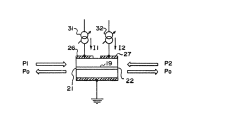
Referring now to Fig. 4, descri?tion will ?roceed to
an optical memory device according to a -,irst embodiment of this
invention. The device comprises a bistable semiconductor laser
which comprises similar pa.rts designated by like reference numerals
and is different from the laser descri'Ded in conr.ection with
Fig, 1 in that one of the electrodes should al-,;ays be separated
or divided into first and second electrodes 26 and 27 with the
counterelectrode left integral as before, In other words, the
laser comprises first and second electro.les 26 and 27 separately
parallel to the active laye~ 19. The first and t'ne second electrodes
26 and 27 are coplanar in principle, It is possible to understand
that the first and the second electrodes 26 and 27 are adjacent
13
to the first and the second ends 21 and 22, respectively, and
vice versa,
In marked contrast to the conventional optical memory
device illustrated with reference to Figs. l through 3, the device
.5 of Fig, 4 co~prises first and second current sources 31 and 32
li~e in the above-cited Odagiri et al report, The first and
the second current sources 31 and 32 are adjustable to supply
first and second injection currents Il and I2 to the active layer
19 through the first and the second electrodes 26 and 27, respectively.
The loss section thereby appears in the active layer 19 although
not positively indicated in Fig, 4,
First and second optical input signals Pl and P2 are
supplied to the first and the second ends 21 and 22, res?ectivel-~,
The optical output signal ~o is emittel from ea-h of the first
and the second ends 21 a.nd 22 as abore, The laser of Fig, 4
has a bistability as will. oe understood 'rom the description
given above with reference to Fi.gs, 1 through 3, It should be
noted ihat the first and the second current sources 31 and 32
serve as two injection current sources for use in individually
controlling the bistability in the manner which wi.ll become clear
as the descri.ption proceeds,
~ eferring again to Figs, 2 (A) and (3), attention will
be directed at first to the fact that it is possible to give
the bistable semiconductor laser similar optical output versus
first and second injection current characteristics and similar
optical output versus first and second optical input characteristics
to the afore-descri`oed gain sections which are provided by the
first and the second electrodes 26 and 27. It will therefore
s~
14
be understood merely ~or brevity of descri?tion that the first
and the second injection currents Il and I2 have the lower and
the upper threshold values i(d~ and i(u) in common, The clear
value l(c), the bias value i(b), and the write value i(w) will
be selected in common to the first and -the second injection currents
Il and I2, The low levels of the first and the second optical
input signals Pl and P2 and the low intensity of the optical
output signal Po are equal to zero and are commo~ to the first
and the second injection currents Il and I2. For the common
bias and write values i(b) and i(w), the bias and -the write levels
Pi(b) and Pi(w) are understood to be common to the first and
the second op-tical input signals Pl and P2 and also to the first
and the second injection currents Il and L2, The high level
Pi(h) will be used in common to the first and the second optical
in?ut signals Pl and P2.
Turning to Figs, 5 (A) throug~h (D), the bistable semiconduc-
tor laser of Fig. 4 has an optical output versus first injection
current characteristic which is depictecl in Fig. 5 (A) and is
similar to the characteristic illustrated with reference to Fig,
2 (A) when the first optical input signal Pl has the low level
of ~ero and furthermore when the second in,jection current I2
is given the bias value i(b). A like characteristic is obtained
betwaen the optical output signal Po and the second injection
current I2 in the manner depicted in Fig, 5 (B) when the second
optical input signal P2 has the low level with the first injection
current Il set at the bias value i(b). The laser has an optical
output versus first optical input characteristic which is shown
in Fig, 5 (C) and is similar to the characteristic described
$~
in connection with Fig. 2 (B) ~hen the second injection current
I2 has the bias value i(b), A similar characteristic results
as depicted in ~`ig. 5 (D) between the optical output signal Po
and the second optical input signal P2 when the bias value i(b)
is given to the first injection current Il.
Referring to Fig, o, it will be assumed that the first
and the second optical input signals Pl and P2 are varied between
the low level of zero and the high level Pi(h) in the manner
depicted along a first or top line and a second line from t'ne
top, respectively, togather with the logic z0ro and one values
0 and 1 represented by the first and the second optical input
signals Pl and P2 '~hen the first and the second injection currents
Il and I2 are varied independently in a timed relation or in
synchronis,n as exemplii`ied llong third and I ourth lines from
the tcp, the intensity of the optical output signal Po varies
in the manner illustrated along a fifth or bottom line, It will
preser.tly be understood that the optical memory device of Fig.
4 is capable of selectively MemorivinO the first and the second
optical input signals Pl and P2.
More specifically referring to Fig, 6, the optical
output signal Po has either the low int0nsity of zero or the
high intensity Po(h) irres~ective of the first and the second
optical input signals Pl and P2 insofar as the first and the
second inJection currents Il and I2 are kept at the bias value
i(b), In the manner which will soon be understood, the intensity
of the optical output signal Po depends on one of the first and
the second optical input signals Pl and P2 that was memorized
in the device before the bias value i(b) is given to the first
16
anl the second injection currents Il and I2, ~,Yhen either or
both o, the first and the second injection currents I1 and I2
is given the clear value i(c), the laser of Fig, 4 i9 reset to
the low stable state A of generating the optical output signal
Po of the low intensity of zero if the laser was in the high
stable state B previous to the decrease of the injection current
or currents to the clear value i(c), The laser is left at the
low stable state A if the laser was previously kept in the low
stable state A,
It will be surmised tnat the second injection current
I2 is decreased at first to the clear value i(c), The optical
output signal Po either falls to the low intensit,, of zero or
i3 kept at the low intensity, '~hen the second injection current
I2 is thereafter increased to the write value i(w), the secor.d
optical input signal P2 is mer"orized in the de~rice, The optical
out ut signal Po keeps the low intensity while the second o?tical
input signal P2 has the low levsl of zero, The o?tical output
signal Po rises to the high intensity Po(h) when t'ne secor.d optical
input signal P2 rises to the high level Pi(h).
In this manner, the bistable semiconductor laser of
Fig, 4 is set by the second optical input signal P2 of t'ne high
level P:l(h), The optical output signal Po keeps the high intensity
Po(h) unti:L the clear value i(c) is given to either or both of
ths first and -the second injection currents Il and I2, As long
25 as the first and the second injection currents Il and I2 are
Icept at the bias value i(b), the intensity of -the optical output
signal Po is not varied by whichever of the first and the second
optical input signals Pl and P2, If the first injection current
17
Il is reduced to the clear value i(c) and then raised to the
write value i(w), the device memori~es the first optica]. input
' signal Pl,
Turning now to Fig, 7, a conventional optical master-slave
flip-flop circuit or device will oe described for a better understand-
ing of an optical master-slave flip-flop device according to
this invention. The conventional circuit comprises first and
second optical memories 36 and 37, each of which is the conventional
optical memory device illustrated with reference to Fig3. 1 through
3. '31ements of the first and the second optical memories 36
and 37 will be referred to by the reference numerals used in
~ig. 1. It ~iill be assumed that the bistable semiconductor lasers
of the respective optical memcries 36 and 37 have a common optical
output versus injection current characteristic and a comm.on optical
output versus input charact~3-istic. The inje-tion cu~rents s~pplied
from the adjustable cur:c~.nt sourct~ 23 of the first and the second
optical memories 36 and 37 ~"ill be called first and second injection
currents and designatt-3d b~ Tl and T2 for distinction from the
first and the second injection currents Il and I2 described above
2~ in con,junction with Figs. ~ through 6,
The active laye~ 19 of the respective bistable semiconductor
lasers of the first and tht3 second optlcal memories 36 and 37
are arran,ged eolinear with an intermediate optical isolator 38
interposed. The first optical memory 36 is supplied i/ith a first
optical input signal Dl from ou~side of the circuit through an
input optieal isolator 39 and generates a first optical output
signal ~1 from each of the first and -the second ends 21 and 22
of the active layer 19, In the manner which will presently be
~27~5~
18
descri~ed, the first optical output signal ~il is con-trolled by
the first in,jection current Tl and depends on the first optical
input signal Dl, The first optical output signal Ql is delivered
~'rom the second end 22 to the second optical memory 37 through
the intermediate op-tical isolator 38 as a second optical input
signal D2,
lt will be assumed throughout the following t~at the
high intensity Po(h) of an optical output signal, such as the
first optical output signal Q1, is not wea~er than the high level
Pi(h) of an optical input signal, Controlled by the second injection
current T2, a secor.d optical output signal ~2 is emitted from
each of the first and the second ends 21 and 22 of the act~ve
layer 19 OI t~e laser of the second optical memory 42. The intermedi-
a~e optical isolator 38 is for preventin~ ths second optical
output signal ~2 from reaching the first optical memory 36 from
the last-mentioned first end 21, ~uch.an optical isolator 38
or 39 is k.nown in t'ne art and is therefore symbolically depicted
in the figure,
Further turni.ng to Fig, 8, the first and the second
injection currents Tl and T2 will oe varied in the manner exempli.fied
along a first or top line and a second line from the top, The
first optical input signal Dl varies between the low ].evel of
zero and the high levul Pi(h) to successively represent (n-l)-th,
n-th, and (n~1)-th optical information X(n-l), X(n), and X(ntl),
each of which is either of the logic zero and one values, During
a time interval to which attention is directed in connection
with the figure, the first optical input signal Dl represents
the (n+l)-th optical information as depicted along a tnird line
19
from t~e top, ~t the begir.ning of -the time interval under considera
tion, it will 'oe assumed that the f'irst optical output signal
Ql or the second optical input signal D2 and the second optical
output signal Q2 reprasent the n-th and -the (n-l)-th optical
information in the manner illustrated along a fourth or penultimate
and a fifth or bottom line, In t'ne optical output signals Ql
and Q2, the optical information X(n-l), ~(n), and X(n~l) is represent-
ed ~ either of the low intensit~ of zero and the high intensity
Po(h) in correspondence to the first optical input signal Dl.
More particularly in i'ig, 8, the first and the second
optical memories 36 and 37 (Fig, 7) keep at first the n-th and
the (n-l)-th optical information with the bias value i(b) given
to thG first and the second injection currer.ts Tl and T2. '~hen
the second injection current T2 is reduced to t'ne clear value
i(c), the second o?tical output signal Q2 is give.1 the low intensity
of zaro no matter whichevar of the low intensity and the high
intensity Po(h) is usad in representing the (n-l)-th optical
information, I~lhen the second injection current T2 is thereafter
increased to the write value i(w), the ~irs-t optical output signal
Ql or the second optical input signal D2 is memorized in the
second optical rnemory 37. T~ne sacond optica]. output signal Q2
re?resents the n-th optical information so long as the second
injection current T2 is not again given the clear value i(c)
and unless the second optichl input signal D2 is changed to represent
different optical inEormation while the second injection current
T2 is given the write value i(w),
l~lhen the clear value i(c) is given to the first injection
current Il, the first optical output signal Ql is given the low
~2~
intensity of 3ero, Irnen the write value i(w) is thereafter given
to the first injection current Tl, the first optical input signal
Dl is memori~ed in the first optical memory 36. The first and
the second optical output signals Ql and Q2 now represent the
(ntl)-th and the n-th optical infcrmation,
Reviewing Figs. 7 a~d 8, the second optical output
signal Q2 would be supplied to the first op-tical memory 36 as
an additional optical. input signal if the intermediate optical
isolator 4& were not used, In this event, A~-D of th~ optical
1~ information represented by the first opti.cal input signal Dl
and by the additional optical input signal is memori~ed in the
first optical memory 36 when the write value i(w) is given to
the first injection current Tl, The intermediate optical isolator
~8 is th_refcre ir.dis?ensabl-, This complicaues the circuitry
and ma:~es it diff_cult to ir.,plement the conventional o?tical
master-sla~e flip-flo? circuit as an integrated circuit,
P,eferrin.g now to Fig, ~, descr:lption wlll be given
as regards an o?tical master-slave flip-flop circuit or device
which is a combination of a pair of optical memories like -the
conventional op-tieal master-slave flip-flop circuit and is a
second embodiment of this invention, The eircuit eomprises first
and seeond opt:lcal memories 41 and 42, each of whioh is the optical
memory device illustra-ted wi-th reference to Figs, 4 through 6.
The current sources of the first and th2 second optical memories
41 and L~2 are, however, somewhat different in the manner which
will shortly be deseri~ed. Other elements of the first and the
seeond optical memories 41 and 42, the elements of the bistable
semiconductor lasers in particular, will be referred to by usir.g
21
the reference numerals used in Fig. 4.
The circuit comprises the bistable semiconductor lasers
of the first and the second optical memories 41 and 42 optically
in tandem, More specifically, the second end 22 of the ac-tive
layer 19 of the laser of the first o?tical memory 41 is coupled
optically directly to the first ~nd 21 of the active layer 19
of the laser of the second optical memory 42, In marked contras-t
to the circuit illustrated with reference to E~'ig, 7, no intermediate
optical isolator is necessary between the first and the second
optical memories 41 and 42. This simplifies the cir^uitry and
f~cilitates implementation of the circuit as an integrated circuit,
The first and the second current sources of the first
and the second optical memories 41 and 42 will be referred to
afresh as .irst through fou-th current sources and designated
by 31 and 32 as before, 43, and 44. The injection currents 3urplied
from the first through the fourth currerlt sources 31, 32, 43,
and 44 will anew be called first throu~h fourth injection currents
and denoted by Il and I2 as above, I3, and I4. The i.n,jection
currents Il -through I4 sarve as clocks for the flip-flop circuit,
The second and the fourth current sources 32 and 44 are f'or giving
the bias value i(b) always to the second and the fourth injaction
currents I2 and I4 and are depicted as constant current sources"
In other respects, each of the first and the second optical memories
4:l and 42 is not dif`ferent from the optical memory device depicted
in Fig. 4.
Turning to ~ig. 10, the first and t`ne third injection
currents Il and I3 will be varied in t'ne manner exemplified along
a first or top line and a second line from the top, The second
and the four'h injection currents I2 and I4 ara given the bias
value i(b) as descri~ed above and depicted along third and fourth
lines from the top. Like in ~'ig, 8, the first optical input
signal Dl successively represents (n~ th and n-th optical informa-
tion X(n-l) and X(n). During a time interval to which attention
is directed in the figure, the first optical input signal Dl
represents the n-th optical information as illustrated along
a fifth line from the top, At the beginning of the time interval
in question, it will be assumed that the first optical output
signal Ql or the second optical input signal D2 and the second
optical output signal Q2 represent the (n-l)-th optical information
in common in the manner depicted along a sixth or penultimate
line and a seventh or bottom line,
~ore particularly referring to ~'ig, 10, it should be
noted at first that the second optical GUtpUt signal Q2 i.s never
memorized in the first optical memory 41 because the second injection
current Il is always kapt at the bias value i(b),
'~hen the first injection current Il is given the clear
value i(c), the first optical output signal Ql is given the low
intensity of zero no matter whichever of the low intensity and
-the high intensity Po(h) i5 had by the (n-l~-th opti.cal information
X(n-l) which is so far kept in the first optical memory 4l,
~hen the write value i(w) is thereafter given to the first injection
current Il, the first optical input signal Dl is memorized in
the first optical memory 41, The first optical output signal
Ql now represents the n-th optical information X(n),
r~hen the third injaction current I3 is given the clear
value i(c), the second optical output signal Q2 is given the
~;~7~S~
23
low intansity of ~ero, ',Ihen the write value i(w) is subsequently
given to the third injection current I3, the second op-tical memory
42 is loaded with the second optical input signal D2, namely,
the first optical output signal Ql.
5 . In this manner, successive control of the first and
the third injection currents Il and I3 makes it possiblè to latch
the first optical input signal Dl in the bistable semiconductor
laser of' the first optical memory 41 and to shift the optical
information X(n) rnemorized in the first optical memory 41 to
-the second optical memory 42, Each of the first and the second
optical memories 41 and 42 now memorizes the n-th optical information,
~ urther turning to Fi r, 11, the first and the second
optis 1 memories 41 ar.d 42 are operable liXe the o?tical memories
30 ar.d 37 (~ig, 7), The -~irst and tha third injection currer.ts
15 Il ar.d _3 ar~ exe;plified along first and second lines, The
second and the fourth injection currents I2 and I4 are al~ays
given Ihe bias value i(b) in the manner depicted along third
and fourth lines, During a time interval under consideration,
the first optical input signal Dl represents the (n~l)-th optical
information X(n~l) as depicted along a fifth line. Ln the manner
described in conjunction with Fig. 8, the first optical out?ut
signal Ql or the second optical input signal D2 and the second
optioal out ut signal Q2 vary as il'lustrated along sixth and
seventh lines.
Referring to Fig, 12, the description will proceed
to an optical master-slave flip-flop circuit or device which
comprises again a pair of optical memories and is a third emoodiment
of this invention. The circuit comprises similar parts designated
~2'7~S~i~
24
by li~e reference numerals, ~le~,ents of the bis-table semiconductor
laser of each of the first and the second op-tical rnemories 41
and 42 will be referred to by using the reference numerals used
in Fig, 4. In contrast to the second and the fourth current
sources 32 and 44 of the circuit illustrated with reference to
Fig. 9, the second and the fourth current sources are adjustable.
Although so different, the second and the fourt'n current sources
will be designated by the reference numerals 32 and 44,
It should be noted in connection with the device depicted
in Fig. 12 that the first and the second optical input signals
Dl and D2 will now be called first and second optical rightwards
input signals. The second optical output signal Q2 emitted from
the first end 21 of the active layer 19 of the oista'ole semiconductor
laser of the second optical memory 42, is delivered as a first
op'isal leftwards input signal Dl' to the sacond end 22 of tne
active layer 19 of the laser of the first optical memory 41.
A second optical leftwards input slgnal D2' is supplied from
outside of the circuit to the second end 22 of'-the activ0 layer
19 of the laser of the second optical memory 42. The circult
is not only operable in response to the first optical rightwards
input signal Dl in the manner described in conjunction wlth Figs.
10 and 11 but also bidirectionally ln res?onse to the second
optical leftwards input si~nal D2' as will be descri'oed in the
following,
Turning to Fig. 13, the first and the third current
sources 31 and 43 (Fig. 12) are adjusted so as to give the bias
value i(b) to the first and the third injection currents Il and
I3 in the manner depicted along a first or top line and a second
s~
line from the top, 'rhe second and the fourth lnjection currents
I2 and I4 will be varied as e~emplified along -third and fourth
lines from the top, Like in Fig, lO, the second optical leftwards
input signal D2' successively represents (n~ th and n-th optical
information X'(n-l) and X'(n), During a time interval to which
attention is directed in the figure, the second optical leftwards
input signal D2' represents the n-th optical information in the
manner depicted along a fifth line from -the top, ~t the beginning
of the time interval under consideration, it will be assumed
that the first and the second optical memories 41 and 42 keep
the (n-l)-th optical information in common, The second optical
output signal Q2 or the first optical leftwards input signal
Dl' represents the optical information X'(n-l) as depicted along
a si~th or penulti~.ate line, The first opt:ical out?ut signal
Ql represents also the optical information .Y'(n--l) as shown along
a seventh or bottom line and is emitted to outside of the circuit
as an ultimate optical output signal of the circuit,
~ lore specifically referring to Fig, 13, it should be
noted at first that the first and the second optical rightwards
input signals Dl and D2 are never memorized in the first ~md
ths second optical memories 41 and 42, This i5 because -the first
and the third injection currents Il and 13 are kept at t~e bias
value i(b),
When the fourth injection current I4 is given the clear
value i(c), the second optical output si.gnal Q2 or the first
optical leftwards input signal Dl' is given the low intensity
of zero no matter whichever of the low intensity and the high
intensity Po(h) is 'nad by the (n-l)-th optical information X'(n-l)
26
which is thus far kept in the second optical memory 42, At -this
instant, t~e first optical left~ards input signal Dl' is not
memorised in the first optical memory 41 because the second injection
current I2 has the bias value i(b), When the f'ourth injection
current I4 is thereafter given the write value i(w), the second
optical leftwards input signal D2' is written in the second optical
memory 42,
~ hen the second injection current I2 is given the clear
value i(c), the first optical output signal 41 is given the low
intensity of ~ero, The second optical output signal Q2 or the
first optical leftwards input signal Dl' now represents the n-th
optical information X'(n), ~hen the second injection current
I2 is subsequently given the write value i(w), the n-th optical
infor.mation X'(n) is written in the first o?tical mamory 41.
Tha n-th optical information X'(n) is Xept in the first and the
second optical memories 41 and 42, In this manner, successive
control of either the first and the third injection currents
Il and I3 or the second and tha fourth injection currents I2
and I4 makes it possible to make the circuit suooessively.memori~e
sele.~ted one of the first optical rightwards and the second optical
leftwards input signals Dl and :D2',
Further turning to F'ig, 14, the first and the second
optioal memories 41 and 42 are not only operable in tha manner
described in oonnection with Fig, 13 but also as in Fig, 11 for
the second optical leftwards input signal D2', The first and
the third injection currents Il and 13 are given the bias value
i(b) in common in the manner depicted along first and second
lines, The second and the fourth injection currents I2 and I4
~2~
are varied as exemplified ~ong third and fourth lines, The
second optical leftwards input signal D2' successively represents
(n-l)-th, n-th, and (n~l)-th optical information X'(n-l), X'(n),
and ,Y'(n~l), In a time interval under consideration, the second
optical leftwards inpu-t signal D2' represents ths (ntl)-th optical
information as shown along a fifth line, In the manner described
in conjunction with Fig, 13, the second optical output signal
Q2 or the first optical left~ards input signal Dl' varies as
exemplified along a sixth line, The first optical output signal
Ql varies in the manner depicted along a seventh line,
R~I erring now to Fig, 15, the description will further
procssd +,o an optical si~nal shifting device which comprises
a plura~ity of the optical master-slave flip-flop circuits and
is a fou-~h er,.bodi.r.~n~ of this invention, In the exar.pl~ being
illustra~sd, ths device comprises first through third optical
master-slave flip-flop circuits 46, 47, and 48, Elements of
each optical master-slave flip-flop circuit will be referred
to by using the reIersnce numerals used in Fig, 9, Elements
of each bistable semiconductor laser of the flip-flop circuits
46 through 48 will be referred to by using like reference numerals
as in Fig. 4,
~ lore partic~ rly, the device includes first through
N-th bistable semiconductor lasers optically i.n tandem where
N represents an even positive integer which is not less than
two, The (n-l)-th and the n-th bistable semiconductor lasers
are arranged optically in tandem with the second end 2Z of the
active layer 19 of the (n-l)-th semiconductor laser optically
directly coupled to the first end 21 of the active layer 19 of
~Z~5~i3L
28
the n-th semicor.ductor iaser where n represents each of 2 through
~ and has no concern with the numoer assigned to -th~; o?tical
informat on such as X(n) or X'(n).
It should be pointed ou-t here in connection ~tith the
optical master-slave flip-flop circuit illustrated with reference
to Figs, 9 through 11 or Figs. 12 through 14 that the first and
the second current sources 31 ar.d 32 are the first and the second
curren-t sources 31 and 32 (Fig. 4) for an odd-numbered bistable
semiconductor laser in Fig. 15, The third and the fourth current
sources 43 and 44 are the first and the second current sources
31 and 32 (Fig, 4) for an even-numbered `ois-table semiconductor
laser. At any rate, a first electrical terminal 51 is connected
in Fig. 15 to the first ^urrent source 31 of each of the first
through the third optical. ~.aster-slave flip-flop circuits 46
to 48. A se^ond electrical terminal 52 is connected to the thirà
current source 43 of each optical master-sl2v3 i`lip-flop circuit.
A control signal generator 53 is for supplying the first and
the second electrical terlr.inals 51 and 52 with first and second
electrical control signals ~1 and ~2 which are variable as will
readily be understood from the fol1.owing.
For the optical signal shifting device being illustrated,
the second and the fourth current sources 3~ and 44 of each optical.
master-slav0 flip-flop circuit areconstant curr0nt sources as
in Fig. 9, hhen Fig. 10 is taken into consideration, it will
readily be understood that the firs-t electrical con-trol signal
~1 can be used in controlling the first current source 31 of
each optical master-slave flip-flop circuit so that the first
optical memory 41 of the first optical master-slave flip-flop
29
circuit 46 may memorize the optical information represented by
the first optical input signal Dl while the optical information
memori~ed in the second optical memories 42 of -the first and
the second optical master-slave flip-flop circuits 46 and 47
are shifted to the first optical memories 41 of the second and
the third optical master-slave flip-flop circuits 47 and 4O,
respectively. The second electrical control signal ~2 can be
used in controlling the third current source 43 of each optical
master-slave flip-flop circuit so that the optical information
memorized in the first optical memory 41 of each optical master-slave
flip-flop circuit may be shifted to the second optical memory
42 of that o-ptical master-slave flip-flop circui,t, In this rnanrler,
the optical signal shifting device is operable to snift the optical
in'ormation successively represented by the first optical in?ut
signal Dl eventually to the second optical memory 42 of the third
optical master-slave flip-,`lop circuit 48. The optical i.nformation
thus shifted to the last-mentioned second optical memory 42 is
represented by an N-th optical output signal, namely, a sixth
optical output signal Q6 in the illustrated example.
Turning to ~'ig, 16, an optical signal shifting device
will be described which comprises similar part3 designated by
like reference numerals and is a fifth emoodi.ment of thi~, invention,
The optical input signal supplied to the first optical memory
41 of the first optical master-slave flip-flop circuit 46, is
the first optical rightwards input signal Dl of tna type descrioed
in conjur.ction with ~'ig. 12, An N-th optical leftwards input
signal (now D6') is supplied to the second optical memory 42
of the third optical master-slave flip-flop circuit 48,
3o
The control signal generator 53 and the first and the
second elec-trical cor.trol signals ~1 and ~2 will now be called
a rightwards control signal generator and first and second rignt~iards
control sig~nals, In the manner described aoove, the first optical
rightwards input signal Dl is shifted to the second optical memory
42 of the third optical mas-ter-slave flip-flop circuit 48 by
the first and the second rightwards control signals ¢l and .~2
produced by the rightwards control signal generator 53,
The device of Fig, 16 comprises a leftwards control
signal generator 55 for generating first and second leftwards
control signals ~1' and ~2'. The second and the fourth current
sources 32 and 44 of each of the first through the third optical
master-slave flip-îlop circuits 46 to 48 are controlled by the
second and the first leftwards control signals ~2' and -~;', respective-
ly, Third and fourth electrical terminals 58 and 59 are supplied~ith the first and the second leftwards control signals ~'1' and
~2' and are connecte~ to the fourth and the second current sources
44 and 32 of each optical ,naster-slave flip-flop circuit.
The device being illustrated, is capaole of le:ftwards
shifting optical signals like the device illustrated with reference
to Fig. 12, It will readily be Imderstood from Fig. 13 that
the device shifts the o~tical information represented by the
sixth optical leftwards input signal D6' to the first optical
memory 41 of the first optical master-slave flip-flop circuit
46, In this manner, the last-mentioned first optical memory
41 produces an optical output si.gnal which may be called a first
optical output signal Ql as in Fig, 12.
31
It is now understood that the optical signal shifting
device of Fig, 16 has a bidirectional stru~ture, namely, a forward
and a backward structure which are identical -to each other,
For example, -the first bistable semiconductor laser of the forward
S structure is the N-th bista'ole semiconductor laser of the backward
structure. The second bistable semiconductor laser of the forward
structure is the (N-l)-th bistable semiconductor laser of the
backward structure, The forward and the backward structures
are equivalent to each other.
Depending on the circumstances, it is possible to understand
the first and the second rightwards control signals ~1 and ~2
as first and second ?redetermined electrical signals, T'ne second
an~ the first leftwards control signals ,~2' and ~1' can be understood
as third and fourth predeter.mined electrical signals, In this
eve,.t, the terminals 59 and 58 may be referred to afresh as third
and fourth electrical terminals, The rightwards control signal
generator 53 can be understood as a first arrangement for supplying
the first and the second predetermined electrical signals to
the first and the second electrical terminals 51 and 52 and the
leftwards control signal generator 55 as a second arrangement
for sup?lying the third and the fourth predetermined electrical
signals to the third and the fourth electrical terminals 59 and
58,
Referring to Fig, 17, description ~ill be given as
regards an optical signal shifting device which comprises a plurality
of optical master-slave flip-flop circuits and is a sixth embodiment
of this invention, Similar parts are designated again by like
reference numerals, The device is not only operable as in Fig,
~2~S~;l
15 but also as in Fig, 16. The second and the fourth current
sources 32 and 44 of each optical master-slave flip-flop circuit
will, however, be presumed to be constant current sourecs as
in Fig, 15,
First through third voltage comparators 61, 62, and
63 are used in conjunction with -the firs-t through the third optical
master-slave flip-flop circuits 46 to 48, respectively, l~lore
particularly, each of the voltage comparators 61 through 63 has
first and second input terminals and an output terminal, The
first in~ut terminal is connected to the second electrode of
each second optical memory 42. The second input terminals of
the first through the third voltage co~parators 61 to 63 are
supplied with a reference voltage Vr of a predetermined voltage
in common,
Turning to Fig, 18 for a short while, it will be assumed
in Fig. 4 t'nat each of the first and the second optical input
signals Pl and P2 has the low level of zero and that the first
injection current Il is Icept at the bias value i(b), The second
electrode 27 has a voltage V which varies with hysteresis versus
the second injection current I2. More specifically, the voltage
V grows generally high when the second injection current I2 is
increased, The volta~e V is, however, kept substantially constant
when the second injection current I2 is increased near to the
upper threshold value i(u), The voltage V again rises when the
second injection ourrent I2 is further increased,
In Fig. 18, the voltage V becomes generally lo~ when
the second injection current I2 is decreased. During the decrease,
the voltage V is kept substantially constant when the second
injection current I2 is decreased near t~ the lower threshold
value i(d) until the second injection current I2 i.s further reduced
below the lower threshold value i(d). It is thecefore appreciated
that the voltage V has higher and lower voltages V(A) and V(B)
when the bias value i(b) is given to the second injection current
I2 and when the bistable semicor.ductor laser is in the low and
the high stable s-tates A and B, respectively,
Turning back to Fig, 17, it will be assumed t'n~t the
first elec-trical control signal ~1 is given a value that makes
the first current source 31 of each optical master-slave flip-flop
circuit produce the first injection current Il of the bias value
i(b), This makes the second optical memory 4', of each optica]
master-slave flip-flo? circuit receive optical. input signals
of the low level of zero from the first optical memory 41 of
that optical master-slave f'lip-flop circuit and also from the
first optical memory 41 of the optical master-slave fli.p-flop
circuit that next follows the flip-fiop circuit in question,
Under t'ne circumstances, comparison of Fig, 17 or 9
with Fig, 4 will show t`nat it is posslble by supplying the fourth
injection current I4 of tne bias value i(b) to the second electrodes
27 of' the second optical mèmory 42 and by cletecting the vol-tage
of the second electrode 27 to Xnow whether tne bistable sem.iconductor
laser is in the low stable state A or in the high stable state
B, namely, whether the optical information kept in the second
optical memory 42 makes the laser generate the optical output
signal of tse low intensity of zero or the high intensity Po(h),
The reference voltage Vr is selec-ted between the higher and tne
lower voltages V(A) and V(B) which are described in con~junction
34
with Fio~ lS, It is possiole with this to me~ke the optical signal
shi.fting device produce in parallel the optical information which
is shifted either righ-twards or leftwards to the second optical
memory 42 of the respecteve optical master-slave flip-flop circuits
46 through 48 and is concurrentl~ Xept therein.
Re~iewing Fig, 18, it will now be assumed in Fig, 4
that each of the first and the second optical input signals Pl
and P2 has the lo~,r level of zero and that the second injection
current I2 is kept at the bias value i(b), The first electrode
26 has a voltage which varies like the voltage V described as
regards the second electrode 27, Higher and lower voltages appear
at the first e'ectrode 26 when the first injection current Il
is also given the 'oias value i(b) and wh0n the bistable semiconductor
laser is in the high and the low stable states A and ~, respectively,
Referring again to rigs. 17 and 13, the optlcal signal
shifting device can produce in parallel the optical information
whic'n is shifted either ri~htwards or leftwards to the first
optical memory 41 of each optical master-slave flip-flop circuit
and is simultaneously kept therein, It should be understood
: 20 in view of the above-described bidirectional structure that such
an optical sginal shifting device is an equivalent of the optical
signal shifting device illustrated with reference to Figs, 17
and 18,
Re~erring now to ~'ig, 19, the description will finally
proceed to an optical signal shifting device which comprises
again a plurality of optical master-slave flip-flop circuits
of Fig~ 9 or 12 and is a seventh embodiment of tnis invention,
Similar parts are designated once again by liXe reference numerals,
The second and the fourth current sources 32 and 44 of each optical
master-slave flip-flop circuit should be adjustable current sources
even when the device is used in only rightwards shifting the
first optical input signal D1,
First through third electrical terminals 66, 67, and
68 are connected to the fourth current sources 44 of -the respective
optical master-slave flip-flop circuits 46 -through 48, A controlled
signal generator 6~ is for supplying first thrcugh third controlled
electrical signals to the respective terminals 6c through 68,
It wi-'l be assumed that the I irst electrical control
signal ~1 is given a value that makes the first current source
31 of each optical master-slave flip-flop circuit produce the
firsl injsction current Il of the bias value i(b), In this event,
the sacond o?tisal rr.emory 42 of each optical master-slave flip-flop
^lrcuit is given o?tical input signals of the low level of æero
from adjacsnt o?tical memories, The bistable semiconductor laser
of each second optical memory 42 therefore has the optical input
versus second injection current characteristic which is sirnilar
to the characteristic described in connection with Fig, 5 (A),
'~hen the first through the third control electrical
signals are given a common value that gives the clear value i(c)
to the fourth i.njection current L4 of each optical master-slave
flip-flop circuit, an optical signal cf the lcw level or intensity
of æero is simultaneously forcibly memoriæed in the second optical
memories 42 of the respective optical master-slave flip-flcp
circuits 46 through 48, 'llhen the controlled electrical signals
are supplied to the first through the third electrical terminals
66 to 68 with another common value t'nat makes the fourth injection
36
current I4 of each optical master-slave flip-f`lop circuit have,
for exam?le, the write value i(w), an optical signal of the high
intensity Po(h) is forcibly memorized in common in the second
optical memories 42 of the respective optical mas-ter-slave flip-flop
circuits 46 to 48.
It is possible in this manner to forcibly set optical
information of the logic zero and/or one value in the second
optical memeroies 42 of` the respective optical master-slave flip-flop
circuits 46 th:rough 4c~ in parallel,
Such optical information may likewise be forcibly set
in the first optical memories 41 of the respective optical master-slave
flip-flop circuits 46 to 48 in parallel, An optical signal shifting
device capa~le of forcibly setting the logic zero and!o:r one
optical information in the first optical m.emories 41 in parallel,
is an equivalent of the optlcal si~nal shiftir.~ device illustrated
with reference to Fig, 19,
l~lhile this invention has thus far been described in
specific conjunction with an appreciaole number of embodiments
thereof, it will now be readily possible for one skilled in the
art to carry this invention into effect in various other manners,
Above all, it should. be clearly understood that the optical
memory device, the optical ma.ster-slave flip-flop device, and
the optical signal shif-ting device are reaclily implemented as
an integrated circuit, The side views so far desscribed should
therefore be understood as lLlustrative of such a device as discrete
devices merely for convenience o description,