Note: Descriptions are shown in the official language in which they were submitted.
1~708~9
84-5-054C
S~TCHED REGULATOR CIRCUIT HAVING AN EXTENDED DUTY CYCLE RA~æE
by
BEIWINDER SI~æH BARN
BACKGROUND OF THE INVENTION
Field of the Invention
The present invention relates to power supplies for electronic
lo circuits and more particularly to a single-ended switched DC voltage or
current regulator having an extended duty cycle range, which is sometimes
referred to in the industry as a "Bed Converter~ (Barn's extended duty
cycle converter).
Description of the Prior Art
The function of a DC voltage or current regulator (also called a
DC converter) is to convert an unregulated source of electrical power
into a source of constant DC voltage or current for an electrical load.
A common design for a single-ended DC voltage or current regulator
employes a transformer to step the voltage or current up or down
dependent upon the specific application. The transformer primary circuit
is opened and closed for a proportionately variable time to meet upon the
power requirements of the transformer secondary circuit. A series-switch
element in the primary circuit provides the basic ON/OFF switching action
to induce a current flow in the secondary. When the primary circuit is
switched OFF it is usually desireable to discharge the energy developed
in the transformer core otherwise unwanted voltage surges can result.
127Q~g
84-5-054C
A technique that is often used to discharge the core when the
primary circuit is open is to employ what is sometimes referred to as a
demagnetizing transformer winding. Such a circuit arrangement is shown
in FIG. 1. The demagnetizing winding discharges the core through the
blocking diode Dl. If the turns ratio of the primary and the demagnetiz-
ing winding are the same, the maximum duty cycle of the circuit for nor-
mal operation is 50%. The ratio of turns on the two windings can be
altered to obtain a larger duty cycle range but at the expense of higher
voltage surges developed across the series switching element. With a 2-
to-l turns ratio a 75% duty is possible but with a consequental voltage
surge on the switch element of three times the maximum input voltage.
This requires a higher voltage-rated switching element than what would
be otherwise required. This is expensive and in some applications, such
as high voltage power supplies, difficult to obtain.
Thus it is an object of the presesnt invention to provide a
switching DC regulator capable of operating over a wide range of duty
cycles with a minimum amount of stress to associated regulator compon-
ents.
It is another object of the present invention to provide a
switching DC voltage regulator capable of operating over an input volt-
age range that varies up to 400%.
It is yet another object of the present invention to provide a
switching DC voltage regulator capable of operating in a single-ended
forward converter configuration.
It is a further object of the present invention to provide a
switching DC voltage regulator that does not use a power transformer
with a demagnetization winding.
l27asss
84-5-054C
SUMMARY OF THE I2 ~ NTION
In order to achieve the above objects of the present invention,
there is provided, for use with a DC switching regulator circuit, a
s circuit to demagnetize the regulator transformer during the period when
the transformer is switched OFF. The regulator uses a transformer in
series with a switching device to cause the primary transformer current
to be switched ON and OFF in response to the power needs of an electrical
load connected to the secondary circuit. A first diode, connected to
the junction of the primary winding and a series switch, conducts the
demagnetizing energy out of the primary circuit into a shunt connected
storage capacitor. A second switching device, operating out of phase
with the first switch, allows the storage capacitor to discharge through
an inductor back to the unregulated input source. A shunt diode between
the inductor and the second FET switch provides a path for the inductor
to discharge through when the second switch opens the path between the
storage capacitor and the inductor.
BRIEF DE5CRIPTION OF THE DRAWINGS
For a better understanding of the invention as well as other
objects and further features thereof, reference is made to the following
description which is to be read in conjunction with the accompanying
drawings wherein:
lZ71[~8~
84-5-054C
FIG. 1 is an electrical schematic diagram of a prior art
technique for demagnetizing the core of a power transformer used in a
regulator circuit.
FIG. 2 is a block diagram of a regulator circuit which embodies
the techniques of the present invention;
FIG. 3 is an electrical schematic diagram of a regulator
circuit which illustrates the present invention; and
FIG. 4 is an electrical schematic diagram which illustrates an
alternate embodiment of the present invention.
DETAILED DESCRIPTION OF THE INVENTION
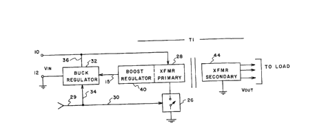
FIG. 2 illustrates a block diagram of the transformer based
regulator circuit 25 which overcomes the shortcomings of the prior art
voltage regulators. (It should be noted that all references to voltage
regulators apply equally to current regulators since eithex parameter
may be detected and stabilized by the present invention.) The input raw
DC supply voltage 10 (Vin) is applied to the primary 28 of transformer
Tl as illustrated. In series with primary 28 is a switch element 26
controlled by an external drive signal applied to leads 29 and 30. The
drive signal may be derived by any number of techniques that sense the
voltage or current parameter at the regulator output (V0utl for
example). As the power needs of the load on the transformer secondary
44 increase, the drive signal increases proportionately the ON time of
switch element 26. The drive signal is also applied to a buck regulator
32 via leads 29 and 34. The output of buck regulator 32 conducts the
demagnetizing current from the transformer primary to the input voltage
supply connected across the input terminals 10 and 12. With the
4--
9~
84-5-054C
additlon of a capacitor and diode (shown more clearly in FIG. 3), the
peimary winding 28 and switch 26 form a boost regulator 40. The boost
regulator 40 provides a means of taking the magnetizing current and
storing it as energy on a capacitor. m e buck regulator 32 removes
energy processed by the boost regulator 40 and delivers it back to the
input source; this assures that the voltage on the capacitor does not
increase indefinitely.
A more precise understanding of the operation of the circuit
may be appreciated in connection with the description of the preferred
lo embodiment shown in FIG. 3.
The advantage of operating at higher duty cycles, as provided
by the circuit of the present invention, is that it reduces the RMS cur-
rents in the primary circuit of transformer Tl and thus their resistive
losses. This is very attractive when FET's are used for the main switch-
15 ing element 26. The large duty cycle range also allows a large inputvoltage range typically available only with a push-pull converter. An
efficient power supply can be made to accept 20V to 60V without requiring
circuit reconfiguration which is ideal for various applications, such as
in telephone central office applications where the supply voltage can be
20 either -24V or -48V nominally.
The block diagram of FIG. 2 is preferably implemented by the
circuit configuration shown in FIG. 3 or FIG. 4. Referring to FIG. 3 an
input power source would be operatively connected to input terminals 10
and 12, while the load to which power is provided is similarly connected
25 to output terminals 14 and 16. A simple AC rectifier and filter 46 is
shown connected to the secondary circuit for illustrating the normal
lZ~39~
84-5-0S4C
application, however, it is not considered part of the invention. The
power transformer Tl is shown with a primary 28 and secondary 44 with
the polarity as is indicated. In series with the primary circuit 28 is
an N-channel FET switch 26. Also connected to the primary circuit is
the boost regulator (shown in FIG. 2 as 40). More precisely a common
boost regulator would consist of the magnetizing inductance of Tl in
conjunction with the transistor switch Ql, steering diode Dl and storage
capacitor C. Connected to the output of the boost regulator 40 is buck
regulator 32. The buck regulator is formed by a P-channel FET Q2, diode
D2 and inductor Ll with the voltage across the storage capacitor C being
the input voltage source to the buck regulator. (Zl and Rl are bias
components for Q2.) The output of the buck regulator is returned to the
input terminal 10 via lead 36. The function of each of these components
is best understood by examining what occurs to the voltages and currents
as Ql and Q2 switch ON and OFF.
An external control signal applied to the gate electrodes of
both Ql and Q2 via lead 29 drives the devices in and out of saturation
causing both to function as simple switches. Since Ql and Q2 are N and
P-channel devices Q2 will be ON when Ql is OFF, i.e. their operation is
complementary. When Ql is ON current flows through the primary winding
28 and Ql to ground. (For purposes of this discussion Vin is assumed
to be a positive voltage.) So long as Ql is ON, Dl remains reversed
biased, since the source-to-drain voltage of Ql is very low. When Ql
turns OFF, the voltage across primary 28 reverses causing Dl to immed-
iately become forward biased. The current in the primary thus goes tocharge C while Ql is OFF. With Q2 ON the current charging C will also
--6--
12'~?89~
84-5-054C
be conducted through Q2 and Ll to the supply connected across input
terminals 10 and 12. The voltage on C adjusts to a value that just
discharges Tl during the OFF time of Ql (during steady state operation).
The net effect of this is to reduce the voltage build up across C (Vc)
and across Ql, and to conserve the dissipated energy through D1 by re-
turning it to the source. When Ql turns back ON and Q2 turns OFF, D2
provides a current path for L1 to dissipate or de-energize the energy
stored therein.
Alternatively Ll and D2 (in combination with capacitor C) may
be functionally viewed as a smoothing filter with an input at terminal
15. The voltage at the junction of Dl and Ql is a square wave. When
Q2 turns on a large potential difference exists between the capacitor C
and the supply terminal 10. Even if Q2 had the current carrying capabil-
ity to handle the surge to the voltage source Vin, (assuming Ll and D2
were not in the circuit) Vc would always be at Vin when Ql initially
turned OFF. This cannot be permitted since it is necessary to apply a
voltage of opposite polarity to the transformer Tl to achieve demagneti-
zation. Thus Vc has to be maintained at some other level than Vin.
The function of buck regulator 32 assures that Vc is at the optimum
level for demagnetization. If Vc rises too high (caused by a change
in the duty) more current would flow through Q2 to the input terminal 10
to bring Vc down to the correct level. And if Vc is initially too
low, then less current would flow through Q2 to increase Vc. In
essence, a self-adjusting effect is provided.
lZ71~ 9
84-5-054C
While the invention has been described with reference to its
preferred embodiments, it will be understood by those skilled in the art
that various changes may be made and equivalents may be substituted for
elements thereof without departing from the true spirit and scope of the
invention. In addition, many modifications may be made to adapt a par-
ticular situation or material to the teaching oE the invention without
departing from its essential teachings.
The circuit configuration shown in FIG. 4 shows a typical
modification that could be made without departing from the spirit of
this invention. In FIG. 4 Q2 is shown as an N-channel device and is
biased through Rl to the drain electrode of Ql via lead 34. This
configuration has the advantage of permitting the regulator to operate
over a slightly wide input voltage range than the regulator circuit
shown in FIG. 3. Zener diodes Zl and Z2 are protective devices
connected across the source-gate channel to protect Q2 from voltage
surges when swltching ON to OFF and OFF to ON. Z2 is sized below the
reverse (breakdown) voltage Vgs f Q2 to insure that Vgs is not
exceeded when Q2 is switched OFF. And, Zl protects the same
gate-to-source channel when Q2 is switched back 0~1.
Finally there may be application where Q2 may be controlled and
biased via an external source (not shown), in which case Zl, Z2, and Rl
may not be required.