Note: Descriptions are shown in the official language in which they were submitted.
~7~
CO~ISTA~IT OUP~REilT CIROUIT~
This invention relates to constant currerlt circuits~ and is
particularly concerned with such a circuit for providing a so-called
sealing current on four-wire transmission lines.
It is known to provide a d.c. sealing current on a four-wire
voice frequency transmission line, in order to maintain a low
resistance at splices and other connection points hy breaking down
small accumulations of dirt and oxides, thereby reducing noise and
other trouble conditions. To this end, a sealing current source is
connected to simplex leads of transmit and receive transforrners
which are coupled to the four-wire line.
Transmission of voice and data signals on a four-wire line
can be impaired by currents which are induced, in the two wires of
each balanced pair of wires of the four-wire line, from external
sources such as a.c~ power lines and transformers. If such induced
currents flow unequally in the two wires, for example due to the
wires having different series or shunt impedances and hence being
imperfectly balanced, then a metallic current exists which can
disturb transmission. Such metallic currents can be minimized by
making the impedance of the sealing current source large relative to
the imbalance in impedance of the two wires. Hence a constant
current circuit, or high impedance current source, is required to
constitute the sealing current source.
Furthermore, as the sealing current is a loop circuit,
flowing in opposite directions on the two balanced pairs of wires of
the four-wire line, it is desirable for the sealing current source
to supply to and sink from the respective wire pairs precisely the
same sealing current.
An object of this invention, therefore, is to provide an
improved constant current circuit, which is particularly suitable
for providing a sealing current on a four-wire transmission line.
According to this invention there is provided a constant
current circuit comprising: first means for passing a constant
current, said first means having first and second terminals; second
means for passing a current, the second means having first and
second terminals and including control means for controlling the
current passed by the second means; a first potential divider
- - - .. . ..
,.
.. ......
: : ; ::
:'. ',, : :,, , '' ': . :: ,` ` '
. , .. .:
. .
:. : .
3L~t~
connected between the first terrninals of the first and second means
and having a tappiny point; a second potential divider connected
between the second terminals of the first and second means and
having a tapping point; and arnpli-fier means responsive to potential
difference between the tappiny points o-f the first and second
potential dividers for controlling the control means, whereby the
current passed by the second means has a predetermined relationship
to the constant current passed by the first means.
Preferably the first and second potential dividers have
equal potential division ratios to their tapping points whereby the
current passed by the second means is equal -to the constant current
passed by the first means.
In a preferred embodiment of the invention, the second means
comprises a transistor constituting said control means, the
transistor having a base coupled to an output of the amplifier
means, a collector coupled to the first terminal of the second
means, and an emitter; and a resistor coupled between the emitter
and the second terminal of the second means. Conveniently, the
first means comprises a transistor having a base coupled to a
reference voltage, a collector coupled to the first terminal of the
first means, and an emitter; and a resistor coupled between the
emitter and the second terminal of the first means.
The circuit preferably includes means for smoothing signals
at at least one of the tapping points.
The invention also provides an arrangement for passing d.c.
sealing current on two balanced wire pairs of a four-wire line,
comprising a constant current circuit as recited above; a first
transformer having a center-tapped winding coupled to one of the two
balanced wire pairs, the center tap being coupled to the first
terminal of the first means; and a second transformer having a
center-tapped winding coupled to the other of the two balanced wire
pairs, the center tap being coupled to the first terminal of the
second means.
The invention will be further understood from the following
description with reference to the accompanying drawings, in which:
Fig. 1 schematically illustrates a known arrangement for
providing seallng current on a four-wire transmission line; and
~:~ , : ' . -
, : ~ . , . : ,: :
.
~Z7~
Fig. 2 schematically illus-trates a constant current circuit
in accordance with an embodiment of this invention for use in
an arrangement as illustrated in FitJ. l.
Referring to Fig. 1, there is illustrated a four-~lire
transmission line comprising two balanced wire pairs 10, 12 for
transmit and receive directions which are coupled via transformers
14, 16 to transmit circuitry 18 and receive circuitry 20 of a voice
frequency (~F) channel unit in a VF carrier transmission system. As
this invention is not concerned with the specific form of the
transmit and receive circuitry 18 and 20, this is not described
further here.
In order to maintain a low resistance at splices and other
connection points on the line 10, 12, a d.c. sealing current is
supplied from a sealing current circuit 22, via a reversing switch
24 by means of which the current direction can be reversed, to
center taps on the windings of the transformers 14 and 16 which are
connected to the line 10, 12. Thus for example a d.c. sealiny
current may be conducted from the circuit 22 via a wire 26~ the
switch 24 and a center tap 28 of the transformer 14 to both wires T,
R of the balanced wire pair 10, this current returning via both
wires T1, R1 of the balanced wire pair 12, a center tap 30 of the
transformer 16, the switch 24, and a wire 32 to the circuit 22.
As already described, it is desirable for the sealing
current circuit 22 to have a high impedance, and hence to act as
both a constant current source and a constant current sink for the
two directions of the sealing current. This invention, an
embodiment of which is described below with reference to Fig. 2, is
concerned with the provision of such a constant current circuit.
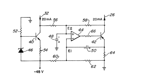
The circuit illustrated in Fig. 2 comprises transistors 40,
30 42; a differential amplifier 44; a zener diode 46; capacitors 48 and
S0; and resistors 52, 54, 56, 58, 60, 62, 64 and 66.
The elements 40, 46, 52, and 54 are arranged in conventional
manner to pass, or sink, a constant current of 20mA from the wire
32, this current value being determined by the zener voltage of the
zener diode 46 and the resistance of the resistor 54. The
` transistor 42 and resistor 64, which has the same resistance as the
; resistor 54, serve to pass, or supply, an equal constant current of
:
:
. - .- . : .
.
.
:. : ,, "
.
~: , .. . .. . , , :
,: , , . . .
:......... , : :, . ,
. .
20mA to the wire 26. The capacitors 48 and 50 serve to filter any
alternating voltages which may be present from outside sources, for
example appearing on the wires 26 and 32 and hence at the collectors
of the transistors 40 and 4Z.
The rernainder of the circuit in Fig. ~ serves to control the
transistor 42 so that i-t acts IS a constant current source as
described above, to pass the same current as the transistor 40. To
this end, the resistors 56 and 58 are connected as a potential
divider between the wires 32 and 26, and the resistors 60 and 62 are
connected as a similar potential divider between the resistors 54
and 64, on the sides thereof which are connected to supply voltages
of -48 volts and ground respectively. The differential amplifier 44
has its inputs connected to the tapping points of these potential
dividers, and its output connected via the resistor 66, which acts
as a current limiter, to the control or base electrode of the
transistor 42.
In operation, the circuit of Fig. 2 serves to maintain
voltages E1 and E2 at the differential amplifier inputs, and hence
at the tapping points of the potential dividers, equal. The voltage
E1 is fixed, for example at -24 volts (half the supply voltage) if
the resistors 60 and 62 have equal resistances, whereby the voltage
E2 is maintained at the same value. Any departure of the voltage E2
from this value is amplified by the amplifier 44 so that a
correction signal i supplied to the transistor 42 to equalize the
voltages E1 and E2.
Considered alternatively, the circuit of Fig. 2 maintains
the voltage dropped across the series combination of the transistor
42 and the resistor 64 equal to the voltage dropped across the
series combination of the transistor 40 and the resistor 54, whereby
precisely the same current is passed to the wire 26 as is received
from the wire 32.
Numerous other modifications, variations, and adaptations
may be made to the embodiment described above without departing from
the scope of the invention as defined in the claims.
,: . : : ,-:
; . ., ::
,; , .. .. ..
.
-. ' : ::::