Note: Descriptions are shown in the official language in which they were submitted.
~7~36~
NON CODED INFORMATION AND COMPANION DATA
SWITCHING MECHANISM
Description of the invention
Field of the invention
The present invention relates to a switching mechanism to be
used in a communication network comprising a plurality of
nodes which may be connected to pure data terminals and to
intelligent workstations able to exchange data and non coded
information NCI such as voice or images.
Background of the invention
Intelligent workstations are able to transmit/receive data and
non coded information which may bej as an example packetized
compressed voice or images.
US patent 4 535 448 describes a system providing the terminals
with the capability of transmitting/receiving both voice data
and pure packetized data. In this system, different types of
interfaces are provided to allow the terminals to have access
~ither to a packet bus dedicated to the exchange of packetized
data or to a time division multiplex bus dedicated to the
~change of voice data. -
.
The system described in this patent does not take advantage of
the present communication network facilities since it~requires
dedicated means for pure data and voice and data handling.
Summary of the invention
An object of the invention is to provide an improved switching~
mechanism to be incorporated in the line scanners of future
communication controllers or 1n an external adapter~which may
be added to the line adapters of existing ~communication ;~
controllers, said mechanism allowing the data~resources of the
FR 9 84 015
... ....
~ ~7096t3
communication controllers to be used for the routing of non
coded information in a communication network.
The mechanism according to the invention allows data and
packetized non coded information NCI, to be exchanged between
woxkstations connected to nodes of a communication network,
said node comprising data handling means (10) for establishing
a session between any origin workstation and any destination
~oxkstation, and for routing the data to be exchanged between
s~id worksta~ions.
Each workstation comprises transmitting means (figure 8) for
arranging the data bits and the NCI bits to be sent into a
woxkstation bit stream format which comprises regular slots
separated by delimitation flags (Fl, F2), each slot being used
to carry, data only bits, NCI only bits or NCI bits and data
bits, the data only slots beginning with a first delimiting
~lag (F2) and the NCI only slots and the data and NCI slots
beginning with a second delimiting flag (Fl) followed by at
least one NCI packet including the addresses of the origin and
~estination workstations involved in a session, the data
portion, if any, following the NCI packet(s) beginning with
tha ~irst flag (F2), and receiving means (figure 9) which are
re~ponsive to the detection of the delimitation flags to
retrieva the data bits and NCI bits in the received bit
stream, -
The network nodes comprise:
a high speed bus (26) onto which the NCI packets areexchanged,
marking means (46, 42) which record the addresses of the
origin and destination workstations and the address of
the node outbound link selected by the data handling
means as a result of the ~initialization phase of a
session which consists in sending routing data inclùding
the addresses of the said:workstations,
FR 9 84 015
~7~
selecting means (40) which are responsive to the
addresses of the workstations contained in the NCI
packets, which are sent once the session initialization
is completed, to get the address of the selected outbound
link for the session from the marking means, and
generating a selection signal therefrom.
Each node inbound link comprises:
NCI receiving means (38),
separating means (34) receiving the bit stream to be
sent by the origin workstation and responsive to the
flag configurations for sending the data bits to the
data handling means and the NCI packets to NCI
receiving means
scheduling means (39) for sending the NCI packets
from the NCI receiving means to the high speed bus,
Each network outbound link comprises:
NCI sending means (48),
gating means ~50) which are responsive to the
selection signal which is active when said~-outbound
link is to be used for connecting the workstations
involved in the session for transferring the NCI
packets from the high speed bus to the NCI sending
means,
formatting means (52) which receives the data bits
from the data handling means (lO) and the NCI
packets from the output storing
means (48~ for arranging them into the workstation
bit stream format.
.
~,,
FR 9 84 015
. ~ ;.~ :
~7~
Brief description of the figures
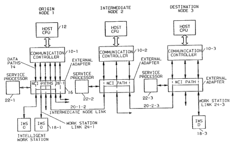
Figure 1 schematically represents three nodes of a
communication network in which the mechanism according to the
invention may be incorporated.
Figur~ 2-A represents the NCI and data bit exchange format on
the workstation link.
Figure 2~B represents the NCI and data bit exchange format on
an intermediate link.
Figure 2-C represents the marking frame data structure on a
workstation link.
Figure 3 represents the block diagram of the external adapter
incorporating the mechanism according to the invention.
Figure 4 represents the block diagram of marking frame
d~tec~or ~6 of figure 3.
~iguEe 5 represents the block diagram of marking output table
4? o igure 3.
Figure 6 represents the block diagram of input circuit 34 of
igure 3. -
~
Figure 7 represents the block diagram of output circuit 52 offigure 3.
Figure 8 represents the block diagram of the transmitting
means in the workstation allowing the bit stream described in
~igures 2-A and 2-C to be generated.
Figure 9 represents the block diagram of the receiving means
in the workstation allowing the data and NCI information to be
retrieved from the bit stream described in figures 2-A and
2-C.
FR 9 84 015
~ ~27~ 3~
Detailed description of the invention
Figure 1 schematically represents a communication network in
which the mechanism according to the present invention may be
incorporated. The network comprises a plurality of nodes, only
nodes 1, 2 and 3 are represented. The components in each node
are referenced with numerals followed by suffixes
representative of the node in which they are incorporated.
Each node comprises a communication controller 10, which may
be an IBM 3725 Communication Controller, a host central
p~ocessing unit CPU 12. The communication controller is
connected to data paths 14 which are bidirectional links
devoted to the transportation of data traffic. According to
the invention, an external adapter 16 connects the data paths
to the users which may comprise intelligent workstations IWS
18 and to intermediate node links 20. For example intermediate
node links 20-1-2 connects node 1 to node 2. These
intermediate node links are high speed time division multiplex
links and are used for transporting the user information from
one origin node to one destination node. The operation of
external adapter 16 is controlled by service processor 22.
~ pecific embodiment of the invention will be described,
~ssuming that the network is of the Systems Network
~rchitecture SNA type. The formats of the messages which may
b~ e~changed in a network of this type are described in the
IBM Systems Network Architecture Reference Summary
G~7-3136-4
~ccording to the invention, the data and NCI information
from/to a workstation 18 are carried on workstation link 24 on
the same channel, which insures a good channel utilization.
NCI information packets are transparently carried between
communication nodes on the intermediate node links, using the
same route as data. Thus, the data and NCI information
~elative to the same workstation are said to be companion. The
route is established through the regular network resources,
* Registered trade mark
FR 9 84 015
;., : .:: ..:
;. ~ ;
~LX~6~
which in the specific described environment comprise the
communication controllers IsM 3725, network control program
NCP, IB~ 370 Central Processing Unit (CPU).
The use of this companion transport is made dynamic which
m~ans that a data session is first opened. This data session
is established using the conventional data communication
network resources for performing the routing and network
management, like if the workstation were a conventional data
ter~inal. Then, NCI transport can take place together with or
without data. A data only transpoxt phase takes place to close
the session.
In each node, the NCI information is carried on the NCI paths
2~ which are schematically represented in figure 1. An
implementation of these paths will be described later on in
more details.
Thi~ prevents the NCI information from being affected by the
v~riable delays introduced by the data paths.
It is assumed that origin workstation 18-1 is to be connected
to destination workstation 18-3. Each external adapters 16 in
the boundary nodes 1 and 3 and in the intermediate node 2 are
abla to route the NCI packets from a given inbound link to the
appropriate outbound link. For example, in node 1 in~ound link
is workstation link 18-1 and outbound link is intermediate
node link 20-1-2.
The frame formats are represented in figure 2.
The NCI packets relative to a workstation are for lnstance
voice packets at 8 kilobits per second and the intermedlate
link 20 is for instance a 64 kilobits per second link. Several
voice packets form different workstations are multiplexed on
~he same intermediate links.
FR 9 84 015
- . .
~7~
The sending workstations mix NCI packets or bunch of NCI
packets with data at regular time intervals for instance at 20
millisecond intervals in order to minimize the delay
distortion ~or one given origin and destination workstation
couple. The NCI packets are delimited by starting flags F1
followed by the origin workstation address WSAO and the
dastination workstation address WSAD and then the NCI
~ontents. The data packets are delimited by starting flags F2
~ollowed by the user data stream. On a workstation link, there
is onl~ one NCI packet relative to the origin and destination
wo~kstation transmitted every 20 millisecond.
In a preferred embodiment of the invention F1 is chosen equal
to the 7E hexadecimal flag (01111110 in binary notation) and
F~ is chosen equal to 7F hexadecimal flag (01111111).
In order to avoid false F1 and F2 flag recognition, the NC~
packets as well as the data packets are sent/received by the
~orkstations using the conventional zero insertion/deletion
techniques.
~uring a first phase, the origin workstation, for instance
l~-l sends data only, structured into frames delimited by
~lags F2 as shown in figure 2 C containing the routing
in~ormation in the data fields. External adapter 16-1
reco~nize the F2 flags delete them and performs ~the zero
deletion to regenerate the real data bit stream to be sent by
the workstation like if it were a terminal directly connec-ted
to communication controller 10 without the e~ternal adapter
During this first phase, the workstation acts exactly as a
data only terminal and sends the appropriate data to a
destination terminal handling data only inside the networkO
Once this regular network routing procedure is completed~ the
dastination workstation 18-3 is able to communicate with the
FR 9 84 015
origin workstation. Then both origin and destination
workstations can exchange data only messages.
Phase 2 is now entered.
The origin workstation sends to the destination workstation a
specific data information as shown in figure 2-B. This
specific data information is:
- seen as a regular data request/response unit RU by the
node resources and then sent to the destination
workstation.
- thanks to a specific coding of a spare bit referenced as
a marking frame bit MF and belonging to the transmission
header TH field of the data frame, the frame is
recognized by the external adapter as an NCI marking
information. This specific bit has no effect on the
regular SNA resources. The general format of the
transmission header TH in the SNA architecture may be
found in the akove referenced document GA27-3136. They
are six transmission header configurations which vary
according to format identifier types FID. FID type 4 is
the most currently used format identifier type. It is
used for traffic between adjacent subarea nodes when both
nodes support explicit and virtual routes. Tr~nsmission
header of the FID 4 type comprises 25 bytes. The first
four bits of byte 0 are coded to 0100 to identify FID 4
format, byte 1 comprises eight spare bits, byte 16
comprises one spare bit and byte 17 comprises eight spare ;
bits.
On all links 14 coming from the communication con*roller 10,
external adapter 16, must recognize, the NCI marking frame
among all data frames it receives from the communication
~ontroller. To do so, external adapter 16 recognizes:
, ~,"
,;
FR 9 84 015
~7~
- the FID 4 identifying bits 0l00 in the first four bits of
byte 0, since the origin workstation uses this format for
its NCI marking frame and other pure data exchanges, and
the marking frame bit MF.
I this marking frame bit MF is found ON, the origin
workstation address and destination workstation address
WSAO and WSAD which are part of the user data are stored
in the external adapter together with the concerned
outbound link 20-l-2.
Phase 3 is now entered.
Now external adapter l6 contains the NCI marking information
and when it decodes the couple WSAO, WSAD it is able to route
the NCI packets from the origin workstation to the appropriate
outbound link, by performing a circuit switching in the
adapter.
During this phase, the format on the workstation link is as
shown in ~igure 2-A
To insure a full duplex communication, the- destination
workstation answers by a data response unit RU and the
operations performed in phases 2 and 3 to mark the route~ ~rom
origin workstation to destination workstation are performed to
mark the route from destination workstation to origin
workstation.
To close the session, a data only phase is entered;to clear
the NCI marking information.
It will now be described in reference to figure 3, the block
diagram of an external adapter. For the sake of clarity, only
the means relative to a communication~from origin workstations~
to outbound links have been represented. However, in order to
perform full-duplex communications, each link has to be
FR 9 84 015
~2~9~
provided with appropriate receiving or transmitting means as
will be explained later on.
In figure 3, only the transmit interface 30-T of the
workstation link 24 of fi~ure l is shown. Two such interfaces
are represented namely, interfaces 30-T1 and 30-T2 relative to
two workstations. The address of the first workstation is
refarenced by WSAOl and the address of the second workstation
is re~erellced by WSAO2. It is assumed that a connection is to
be established between these workstations with destination
~rkstations the addresses of which are WSAD1 and WSAD2
respectively. These connections will be established using the
pxocedure described above through the receiving interfaces
32-Rl and 32-R2 of outbound intermediate links 20. The
outbound links are selected using the conventional network
procedures, during the data only phase transport (phase l) and
have the outbound link addresses OLAl and OLA2.
In this figure, the components interface have a general
reference number and a suffix l or 2 which indicates that the
component is involved in a connection initiated by the origin
~orkstation having the address WSAO l or WSAO 2.
The interface 30-T is connected to input circuit 34 which
separates the data and NCI information received from the
workstation, delete the F2 delimitation flags inserted in the
information flow by the workstation as shown in figures 2-A to
~-C and delete t~e zeroes which were inserted in the data and
:
NCI packets.
The data bits are sent to communication controller 10 though
data input line 36 at the link clock xate. The NCI packets
including the delimiting Fl flags, the address of the orlgin
and destination workstations WSAO, WSAD and the NCI packets
are stored in a first in-first out~input memory memory 38. The
information read out from memory 38 on bus 54 is provided to
outbound link selector 40.
.~:
FR 9 84 015
~27~
The F1, WSAO-WSAD fields and NCI packets which are read from
memory 38 are provided to NCI path 26 under control of bus
scheduler 39 to be routed to the appropriate ou~bound receive
interface 32-R. The selection of the outbound receive
interface is done by outbound link selector 40.
ing the second phase of the session, marking output table
~ is loaded with the address couples WSAO-WSAD and the
corresponding outbound link address OLA. Table 42 is a content
a~dressable memory which is addressed by the WSAO-WSAD
~o~lples .
The output data line 44 is provided to marking frame detector
~ hich retrieve in the data stream, from communication
controllers 10 the address fields containing the address
couples WSAO-WSAD. Thus, during the second phase of the above
described process, detector 46 associated to each data output
line ~4 loads the table in memory 42. The NCI packets on bus
~6 are provided to output first in-first out memory 48 through
~ND gate 50.
~utput circuit 52 receives the data stream from output data
line ~ and the information read from memory 48 under control
~ the 20 millisecond clock. Circuit 52 provides on the
r~c~ive interface of the outbound intermediate link the
~ata/NCI packets stream such as shown in figures 2~ to 2-C.
To do this, it adds the appropriate flags and performs the
~ero insertion function.
The address couples WSAO-WSAD read from input first in-first
out memory 38 are provided to outbound link selector 40,
through bus 54 which causes marking output table to be
addressed through bus 56. The corxesponding outbound link
address OLA read from table 42 is provided to selector 40
through bus 58 and is used for providing a conditioning signal
to the appropriate AND gate 50 throuqh line 60.
~R 9 84 015
127~ 0
As represented in figure 3, input FIFO memory 38 is used by
only one workstation, thus during each 20 millisecond period,
it only contains one NCI packet, whereas output FIFO memory 48
may contain NCI packets relative to a plurality of
ori~in/destination workstation couples, since as described
above, the intermediate links are multiplex links.
To insure full duplex communication, each workstation link 24
in figure 1 comprises transmit interfacing means 30, 34, 36,
38 and receive interfacing means which are similar to 46, 50,
~8, 52. Each outbound link 20 in figure 3 comprises receive
interfacing means 46, 50, 48, 52 and transmit interfacing
~eans ~hich are similar to 30, 34, 36, 38.
Ma~Xing frame detector 46 will now be described in reference
to figure 4. It works under the control of the data link bit
clock signal provided by output circuit 52 (as will be
described later on in reference to figure 6) on line 70. The
data bits on output data line 44 are inputted into one's
~ounter 72 at the data bit clock rate. The content of counter
7~ i~ compared by comparator 74 with the value six. The
received data bit on line 44 is inverted in inverter 76. The
Ol~tpUt of inverter 76 and the output of comparator 74 are
provided to AND gate i8. Thus AND gate 78 provides an active
~utput signal when six ones followed by a zero have been
detected in the data stream. The active output signa-~ from AND
gate 78 on line 80 set flag detection latch 82 and is used as
general reset signal.
Output line 84 of latch 82 and data bit clock line 70 are
connected to the inputs of AND gate 86. The output of AND gate
86 is provided to counter 88.
Thus when latch 82 is set, lndicatinq that an SDLC f flag has
been detected in the input data stream, counter 88 begins the
data bit period counting. Comparator 90 compares the counter
content with parameter NTH which indicates the beginning of ;
the transmission header TH with respect to the end o~ the flag
FR 9 84 015 ~ ;
f (see figure 2-C). The value of parameter NTH is loaded into
register 92 by external service processor 22.
T~l~ data bits on line 44 are inputted into 16-bit shift
register 94. The content of register 94 is compared by
comparator 96 with the FID 4 type bit configuration. The
output line 98 of comparator 96 and the output line 100 of
comparator 90 are provided to AND gate 102. When the output
signal on output line 104 of AND gate 102 is active, i.e. when
the FID 4 configuration has been detected in the transmission
header, FID 4 det~ction latch 106 is set. The signal on output
line 108 of latch 106 is provided to the reset input of f flag
detection latch 82 and to one input of AND gate 110. The other
input of AND gate 110 is connected to data bit clock line 70,
thu~ AND gate 110 provides on its output line 112, the data
bit clock pulses from the time when the FID 4 configuration
has been detected, The output line 112 is provided to counter
114 which begins to count the data bit clock periods.
The content of counter 114 is compared with parameter NMF
~hich indicates the position of the marking bit MF with
~espect to the end of the FID 4 configuration. This parameter
i~ loaded into register 116 by service processor 22 and
p~-ovided to comparator 118 together with the content of
counter 114.
The content of register 94 is compared by comparator 120 with
a masked configuration allowing the~MF bit to be detected.~
Output line 122 of comparator 118 and output line 124 of
comparator 120 are provided to AND gate 126~which provides an
active signal on its output line 128 when the MF bit is
d~tected. This signal~sets MF detection latch 130.
OUtput line 132 of latch 130 and~data bit clock ~line 44 ~are~
provided to AND gate 134, which thus~ provides on its output
line 136 the data bit clock~slgnal~to counter 138. From~the
time when MF bit is detected, counter 138 begins~to count the
:
FR 9 84 015
~2~
14
data bit clock periods. The content of counter 138 is compared
by comparator 142 with parameter NWSA which is loaded in
register 140 by e~ternal processor 22.
Parameter NWSA indicates the position of the address fields
with respect to the position of the MF bit. Thus, when an
equality is detected by comparator 142, a load control signal
is provided on output line 144. This pulse causes the content
o~ register 94 to be loaded into WSAO-WSAD register 146 and
the corresponding outbound link address OLA to be loaded in
register 148.
The OLA parameter is contained in register 150 in which it is
loaded by service processor 22.
Latch 82 is reset by the output signal on output line 108 of
FID 4 detection latch 106. Latch 106 is reset by the general
reset signal on output line 80 of AND gate 78 or by the signal
on output line 132 of latch 130. To do this, line 80 and line
13~ are provided to the inputs of OR gate 152, the output line
o~ ~hich is provided to the reset input of latch 106. Latch
13Q is reset by the general reset signal on line 80 or by the
si~nal on output line 144 of comparator 142. To do this, lines
~0 and 144 are provided to the inputs of OR gate 154, the
output line of which is provided to the reset input of latch
130. -
~
~arking output table 42 and its peripheral circuits will nowbe described in reference to figure 5.
Contention resolution circuit 180 receives the load signals
generated on lines 144 of the mar~ing frame detectors 46 of
the e~ternal adapter.
It generates on one of its output lines 182, a selection
signal which is active to perform the updating of output
marking table 42 for a specific interface 32. -
~ '~
FR 9 84 015
~7~
AND gates 184 are conditioned by the selection signals on
lines 182 for gating the content of WSAO-WSAD registers 146
provided from busses 156 shown in figure 4. The output busses
186 of AND gates 184 are provided to OR gate 188, which
provides on its output bus 190, the WSAO-WSAD information to
be stored in table 42.
~N~ gates 192 are also conditioned by the selection signals on
line 182 for gating the content of OLA registers 148 provided
~rom bus 160 (figure 4) to their output busses 194. The output
busses 194 are provided to OR gate 196 which transfers the
content of the selected OLA register 148 to marking output
table 42 for updating.
The selection signals on lines 182 are provided to OR gate
~0~, the output signal of~which on line 202 activates counter
~ddress sequencer 204. Counter address sequencer provides on
it~ o~ltput bus 206, the address of the position in table 42 at
which the WSAO-WSAD and corresponding OLA information has to
be written.
T~bl~ ~2 is read under control of circuit 40 (figure 3) which
r~ceives the information from the input first in-first out
memories 38. The information read from these memories on
busses 54 are provided to addressing circuit 208 which
recogni~e the F1 flags preceding the WSAO-WSAD field~.
:
~s schematically shown in figure 5, addressing circuit 208
comprises for each inbound link 30, input register 210 into
~hich the information read from first in-first out memory 38
is inputted from bus 54. Circuit 212 detects whether register
210 contents` a flag Fl or not. If yes latch 214 is set in
order to condition AND gate 216 during the time the following
fields WSAO~WSAD are read. During this time the content of
register 210 is provided to address selector 218.
Address selector 218 selects one of the address couples
~SAO-WSAD provides by the AUD gat~s, which is inp~tted lnto
FR 9 84 015 ~ ~
- . . ~.... . .
~7~
16
memory address register 220 by means of bus 222. Thus input
address register provides on bus 56, the address of the memory
location, to be read~ The corresponding OLA address is
provided to register 224, decoded into decoder 226 which
provides on one of its output lines 60, a signal which is
active to condition the appropriate AND gate 50 (figure 3).
Input circuit 34 will now be described in reference to figure
6. This circuit performs the data and NCI separation function
and deletes the F2 flags and the zero following five ones.
The bit stream received from inbound link 30 is inputted to
shift register 240. The content of register 240 is compared
ith Fl and F2 flag patterns in circuits 242 and 2440 The bit
stream which is shifted out register 240 on line 246 is
provided to zero deletion circuit 248 the function of which is
to delete the zero following five ones. This operation is
inhibited when the Fl and F2 flags are detected by means of OR
circuit which receives the output signals from circuits 242
and 244 and provides on its output line an inhibit signal
which is active to inhibit the zero deletion function.
:
Th~ active output signal from circuit 242 on line 254 sets
latch 256, which thus provides an active signal on its output
~58 during the periods corresponding to NCI received bits.
.
Th~ active output signal from circuit 244 on its output line
~45 is provided to latch 260, which thus provides an active
signal on its output 262 during the periods corresponding to
data received bits.
The bit stream from zero deletion circuit on line 264 is
provided to AND gates 266 and 268 which are conditioned by the
NCI and data period signals on line~s 258 and 262 respectively.
Latch 256 is reset by the active signal on line 245 and latch
~60 is reset by the active slgnal on line 254. `
:
FR 9 84 015
.. ,. - . ~ , .
~ ~ 7~3~
The active output signal from circuit 244 sets latch 270 which
is reset eight bit later, so as to provide on its output line
~72, a signal which is active during the F2 flag periods. This
signal is inverted in inverter 274.
Th~ link clock is provided to AND gate 278 which is
conditioned by the active signal on data period line 262 and
the ~ctive signal on output line 280 of inverter 274. AND gate
278 provides the data clock bit signal on its output line 282
~uring the data only periods. This signal controls the sending
of the data bits to communication controller 10.
The Fl flags, WSAO and WSAD fields and the NCI packets are
pl~ovided to first in first out memory 38 by AND gate 266. The
d~ta bits are provided to communication controller 10 by AND
~ate 278.
~utput circuit 52 will now be described in reference to figure
7. This circuit generates the data and NCI bit stream on
outbound link 32-R.
Th~ information read from the output first in-first out memory
48 is provided to input register 300, the content of which is
ifted at the outbound link clock rate and is provided
~hrough line 302 to one input of AND gate 304. AND gate 304 is
c~nditioned when there is an active signal on its seeond input
line 306. This signal is generated by NCI packet control
circuit 308 which controls the unloading of output first
in-first out memory 48. At each 20 millisecond periods, it
allows the memory content to be unloaded and then a data
period to be entered. Thus: it provides a signal which is
active during the NCI periods on line 306 and a signal which
is active during the data periods on line 310.
When signal on line 3].0 becomes active, latch 312 is set
during eight bit periods, and provides an active output signal
on its output line 314 which`activates F2 insert circuit 316,
FR 9 84 015
.. . . . . .
~7
18
Data period signal on line 310, the link clock signal on line
318 and the output signal from latch 312 inverted in inverter
320 are provided to AND gate 322, which thus provides on its
output line 70, the data bit clock signal which controls the
sendins of the data bits from communication controller 10 and
the operation of marking frame detector 46. The data bit
stxe~m from controller 10 on line 44 are provided to one input
o~ ~R ~ate 324 at the rate of the data bit clock on line 70.
Tlle second input of OR gate 324 is connected to output line
3~6 of AND gate 304. Thus OR gate 324 provides the data and
memory 48 content during the appropriate periods, to zero
insertion circuit 328.
Output line 330 of circuit 328 is connected to one input of OR `i
~ate 332.
When latch 312 is set, indicating that a data period is
~ntel-ed, flag F2 is sent by F2 flag insert circuit 316 on the
~econd input line 334 of OR gate 332. Thus OR gate 332
provides on the outbound link 32-R, the data and NCI stream as
described in reference to figures 2-A to 2-C.
Fl ~lag configuration in the information read from memory 48
is detected by circuit 334. The output signal from of circuit
33~ sets latch 335 which provides on its output line 336 an
inhibit signal which prevents a zero to be inserted by circuit
328 when flag Fl is read from memory 48 to be sent to outbound
link 32-R. ::~
In addition to the conventional data and NCI handling means,
the workstations comprise transmitting means (represented in
figure 8) for generating the bit stream to be sent to the
transmit interrace 30-T of the node inbound link and réceiving
means (represented in fi~ure 9) for retrieving the data and
NCI bits from the bit stream on the receive interface of node
outbound link 30-R. The conventional data and NCI handling
means are not shown in figures 8 and 9.
~R 9 84 015
~ ., . ~ .
. :.,, . , ,:.,
~ ~7~9~;iO
19
The transmitting means shown in figure 8 are similar to
circuit 52 shown in figure 7 since they substantially perform
the same function, and the receiving means shown in figure 9
are similar to circuit 34 shown in figure 6 since they
substantially perform the same function.
The transmitting means shown in figure 8 comprises data and
N~I lines 400 and 402 which receive the data bit stream and
th~ NCI packets to be arranged into the stream shown in figure
2-~ to ~-C.
The data bits are provided on line 400 at the rate of the link
clock signal generated on output line 406 of AND gate 404.
~he ~CI packets are provided to circuit 408 which generates on
output line 410 a signal which is active when there is a NCI
p~cket ready to be transmitted and a signal on output line 412
~h~n no NCI packet is ready which corresponds to a data
period.
~ND gate 414 is conditioned by the active signal on output
line 410, at the next 20 millisecond period. The active signal
on output line 416 sets latch 418 which remains set during
~ight bit periods and is then reset. The active signal on
output line 419 of latch 418 activates Fl insert circuit 420
which causes the Fl flag to be sent to input line-422 of OR
circuit 424.
Output line 419 of latch 418 is provided to inverter 426,
output line 428 of which is provided to one input of AND gate
430, which is thus conditioned, when NCI packets have to be
sent after the flag Fl insertion. The second input line of AND
gate 430 is line 402. Thus AND gate~430 provides on its output
line 432, the NCI packets to be sent on interface 30-T, at the
link clock rate. To do so, the link clock signal is provided
to AND gate 431 which is conditioned by the output signal from
latch 426, and which provides on its ouput line 433, the NCI
clock signal.
' : ~
FR 9 84 015
. ~ . "
,., , ,, . ~ ,
~7~
When the signal on data period line 412 is active, latch 434
is set, and remains set during eight bit periods~ The output
line 436 of latch 434 is provide to one input o~ OR gate 438.
The second input of OR gate 438 is connected to output line
440 of ~ND gate 442. AND gate 442 is conditioned during the
da~a only period to provide an active signal on its output
lin~ 440 at each 20 millisecond period. Thus OR gate provides
an aotive output signal on line 444 when F2 flags have to be
inserted as shown in figures 2-A and 2-C.
This signal activates F2 flag insert circuit 446 which causes
the F2 flag to be sent to input line 448 of OR gate 424.
The output signal from latch 434 is inverted in inverter 450,
and output line 452 of inverter 450 is provided to one input
o~ ~D g~te 404. Thus AND gate 404 is conditioned during the
data period when flag F2 is not to be inserted to provide on
its output line 406, the link clock signal at which rate the
~ta bits are sent to line 400.
/
ata bits on line 400 and the NCI packets on line 432 are
pl~avided through OR gate 454 to zero insert circuit 456, which
~ovides on its output line, the data and NCI packets to input
line 458 of OR gate 424.
~`
ThP ~ero insertion function of circuit 456 is inhibi-ted, when
Fl and F2 flags have to be sent. This is done by the inhibit
si~nal which is provided by OR gate 460 on line 462. The
input lines of OR gate 460 are lines 419 and 444 which provide `:
active signals when the flags have to be inserted in the bit
stream, to be sent on interface 30-T.
Thus OR gate 424 provides on its output line 30-T, the bit
stream shown in figures 2-A and 2-C.
~s shown in figure 9, the bit stream received by a workstation
on interface 30-R is provlded to~input shlft re`gister 500.
' ~
:,
FR 9 84 015 ~ ~ ~
~L~7a~
The content of register 500 is compared with F1 and F2 flag
patterns in circuits 502 and 504. The bit stream which is
shi~ted out register 500 on line 506 is provided to zero
deletion circuit 508 the function of which is to delete the
zero following five ones. This operation is inhibited when the
Fl and F2 flags are detected by means of OR circuit 510 which
recei~es the output signals of 502 and 504 and provides on its
output line an inhibit signal which is active to inhibit the
2ero deletion function.
The active output signal from circuit 502 on line 514 sets
latch 516, which thus provides an active signal on its output
513 during the periods corresponding to NCI received bits.
The active output signal from circuit 504 on its output line
515 is provided to latch 520, which thus provides an active
~ignal on its output 522 during the periods corresponding to
~ta received bits.
The bit stream from zero deletion circuit 508 on line 524 is
provided to AND gates 526 and 528 which are conditioned by the
NCI and data period signals on lines 518 and 522 respectively.
:
Latch 516 is reset by the active signal on line 515 and latch
5~ is reset by the active signal on line 514.
The active output signal from circuit 504 sets latch 530 which
is reset eight bit later, so as to provide on its output line
532, a signal which is active during the F2 flag periods. This
signal is inverted in inverter 534.
The bit clock is provided to AND gate 538 which is conditioned
by the active signal on data period line 522 and the active
signal on output line 540 of inverter 534. AND gate 538
provides the data clock bit signal on its output line 542.
This signal controls the sending of the data bits from output
line 544 of AND gate 528 to the data handling means of the
workstation.
F~ 9 84 015
-~ ~ ' ', ', '
~7t)~
22
AND gate 526 has a third input line 546. This line is
activated when a F1 flag is detected by circuit 502. To do
this, latch 548 is set when. F1 flags are detected and reset
eight bit periods later, latch 548 provides an output signal
which is inverted in inverter 550. Inverter 550 provides on
its output line 546, the inhibit signal to AND gate 526.
Tl~us ~ND gate 536 provides on its output line 552 the NCI
packet bits which are sent to the NCI handling means of the
workstation.
:
'
: ~
::
::
FR 9 84 015