Note: Descriptions are shown in the official language in which they were submitted.
63
STACXED CIRCUIT CARD AND GUIDED VE~ICLE CONFIGURATIONS
1 BACKGROUND OF THE INVENTION
The present invention relates to multiple circuit
card configurations which provide efficient space uti-
lization, electrical continuity between adjacent circuit
boards and cooling of the electrical components mounted on
the cards for such applications as missile electronics
units.
For most applications, the size of the electrical
circuit cards on which the electrical components are
mounted in an electronics unit is limited by packaging
constraints and ~he like. As a resul~, multiple circuit
boards or cards are employed in close-packed arrangements.
One such application is that of guided vehicles, such as
missiles or torpedos, wherein the guidance electronics
unit is pacXaged within the relatively narrow tubular
configuration of the vehicle body. A number of circuit
cards are typically employed to comprise the electronics
unit. In conventional arrangements, multiple pin connec-
tors are located on one edge of each circuit card. These
connectors are then mated to matching connectors on a
"motherboard" which provides a means to electrically
couple power and siynals between the various cards. For
missiles, the motherboard is typically aligned parallel to
but offset from the longitudinal:~axis of the missile, with
~5 the circuit cards being arranged perpendicular to the
longitudinal axis of the missile. The motherboard is
supported by elongated~ rails extending along the missile
sides, and the circuit cards are supported by the
^ ' ~
- , , ,,; , , .: .. .. . , :
. . , . :; . :: .
~2~ 63
1 connectors and by card guides secured to the rails. A
significant disadvantage of this approach is that the
number of connector pins is limited by the confined area,
and the assembly and testing operations are necessarily
S complex. The configuration also wastes much of the
available space, and the pin connectors required are quite
expensive. Moreover, the configuration is not conducive
to reliable operation in applications wherein the circuit
card arrangement is subjected to high G forces.
The ~lectronics sections of missiles are ~ypically
exposed to high G forces, and the circuit cards, connec-
tors and related hardware must be structurally adapted and
secured to withstand such forces while providing satisfac-
tory electrical performance. Because the circuitry is
typically arranged in a plurality of closely packed boards
with relatively high power output, severe heat dissipation
requirements are also common.
Two approaches have been used in the past to meet
the severe heat dissipation requirements of missile
electronics units. Both approaches employ ceramic circuit
cards which are difficult to repair and are easily damaged
in removal. The first involves an active cooling tech-
nique wherein a fluid is circulated through a plate on
w~ich the circuit card is mounted. This approach requires
~5 a complex cooling system, and conventionally depends upon
bonding of frangible ceramic cards to the coolant plate to
provide the necessary thermal conductivity. The cooling
achieved by this approach is typically not uniform, the
bonds do not-provide high heat conductivity, and repair is
difficult. The second approach is to provide passi~e
cooling to the ceramic cards by bonding them to metallic
heat sinks, typically aluminum. This approach also has
the drawbacks of non-uniform cooling, low conduc~ivity of
the bonds, and difficulty of repair, and in addition is
highly weight inefficient.
, ' .,' ~'..: : :'
:, . : .: .: .
~7~163
1 In conventional guided vehicle or missile config-
urations, the seeker platform supporting the seeker
elements is located at the forward region of the missile,
and is separated from the aft missile body by the elec-
S tronics unit. The boresight of the seeker platform must
be properly aligned with the aft missile body to provide
accurate missile guidance and con~rol. The alignment is
typically achieved by mechanical means, such as shimming
the platform as it is secured to the structural rails to
achieve a parallel alignment between the platform and a
corresponding parallel surface of the aft missile section,
while the assembled missile is mounted on a test fixture
for optical or RF measuremen~s. The alignment procedure
is time consuming and adds significantly to the cos~ of
the missile assembly.
It would therefore represent an advance in the art
to provide a circuit board configuration which provides a
simple, low cost means of interconnecting multiple cards
in an `electronics unit without the use of conventional pin
connectors, while providing an increased circuit board
area.
It would further be advantageous to provide a
multiple circuit card configuration which provides a
simple and low cost means or cooling the electrical
~5 components mounted on the circuit cards.
It would further be advantageous to provide a guided
vehicle configuration which substantially eliminates the
need for expensive boresighting tests and procedures to
align the seeker platform with the aft vehicle body.
SUYYA~Y OP ~E INVENTION
An improved circuit card configuration is disclosed.
The configuration includes a plurality of stacked circuit
cards, each having a central opening formed therein. Each
card has an electrically conductive pattern formed there-
on, including a plura~ity of conductive pads disposed on
"
. : - . ~ -
3~;~1'~3963
1 each side of the card adjacent the inner and outer peri-
pheral edges. Means are provided for supporting the
respective inner and outer peripheral edges of the circuit
cards so that the cards are in a stacked, parallel
S relationship. A plurality of inner and outer metal-on-
elastomer connectors are arranged to respectively connect
corresponding conduc~ive pads of adjacent peripheral edges
of the circuit cards and to electrically connect ~he
stacked circuit cards. In accordance with one aspect of
the invention, the inner conductors are employed to
provide electrical power to the circuit cards, and the
outer connectors are employed to couple time-varying or
information signals between the cards, ther~by isolating
power and signal lines.
In accordance with another aspect of the invention,
means are provided for enclosing and sealing the circuit
cards to form a sealed unit. A coolant fluid is disposed
within the sealed unit in contact with the circuit cards
and the electrical components populating the circuit
~0 cards. The coolant fluid absorbs heat from the components
and circuit cards and comprises a passive cooling system.
A further aspect of the invention is a new guided
vehicle configuration r such as a missile or torpedov for
carrying an electronics unit such as ~he circuit card
configuration described above. The configuxation includes
a substantially cylindrical aft vehicle section carrying
the vehicle propulsion system. A tubular center struc-
tural member is secured to the aft section and ex~ends
forwardly therefrom. A tubular vehicle outer cover member
is provided. A vehicle electronics unit fits within the
outer cover member and has a central opening formed
therein, the electronics unit being assembled with the
tubular structural member extending through the central
opening formed therein. The forward sensor section of the
vehicle includes a sensor platform with a central opening
, ",
... ~ ,
: : ,... ..
~.: ::.' . ,
.,
: .
6~
formed therein. These various components of the vehicle
are assembled ~ogether, with the tubular support member
extending through the respective openings in the
electronics unit and the sensor platform. A fastener
coupled to the forward end of the central tubular
support is used to secure the assembled components in
position.
Other aspects of this invention are as followso
A cooled electronics unit, comprising:
a plurality of electrically interconnected circuit
cards populated with electrical components;
means for enclosing and supporting said plurality
of circuit cards to form a sealed unit; and
an electrically non-conductive coolant liquid
selectively disposed within said sealed unit adjacent
preselectad circuit cards in direct contact with areas
of said preselected circuit cards and with said
components so as to absorb heat generated by electrical
power dissipation.
A cooled electronics unit, comprising:
a plurality of circuit cards populated with
electrical components, each having an outer periphery
defining the outer edge thereof and an inner edge
surrounding an interior opening in each circuit card;
said circuit cards comprising an electrically
conductive pattern for electrical connection of
~lectrical components mounted thereon and comprising a
plurality of conductive elements disposed adjacent said
outer periphery;
first support means for supporting said outer
periphery of said circuit cards in an aligned
relationship;
second support means for supporting said inner
peripheries of said circuit card~ in an aligned5 relationship;
first interconnection means for selectively
electrically connecting predetermined ones of the
conductive elements adjacent said outer periphery of
' :' : : .,~ :'' ~ .
::
:~ . - ,: ::.
. " ' ~:: ' ~ ' ' '
, ,.,
' : . ~ ,
5a
~7~
adjacent circuit cards;
means for enclosing said circui~s, said support
means and said interconn~ction means to form a sealed
electronics unit; and
an electrically non-conductive coolant liquid
selectively disposed within said sealed unit adjacent
preselected circuit cards in direct contact with areas
of said preselected circuit cards and with said
components so as to absorb heat generated by electrical
power dissipation.
BRIEF DESCRIPTION OF TH~_DRAWINGS
These and other features and advantages of the
present invention will become more apparent from the
following detailed description of exemplary embodiments
thereof, as illustrated in the accompanying drawings, in
which:
FIG. 1 is a simplified cross-sectional view of a
preferred embodiment of a stacked circuit card
configuration embodying the invention, utilizing shaped
memory alloy closure rings to efPect a hermetic seal
around the circuit card stack to contain an inert
coolant fluid.
FIG. 2 is a partial cross-sectional view taken
along line 2-2 of FIG. 1, illustrating the fluid vent in
the fill tube structure.
FIG. 3 is an enlarged view of the portion of the
circuit card assembly of FIG. 1 which is enclosed by
circle 3 of FIG. 1.
FIG. 4 is a plan view of the circuit card
configuration o~ FIG. 1, taken along line 4-4 of FIG. 1
FIG. 5 is a cross-sectional view taXen along line
5-5 of FIG. 4 illu trating the position registering pin
for rotational and stacking alignment of adjacent
circuit cards.
FIG. 6 is an enlarged view of the structure within
circle 6 of FIG. 1 illustrating the relative positioning
o~ the elastomeric connector and the adjacent circuit
cards.
.
~,; ;:, ,
' '
,. .,
.
963
1 FIG. 7 is a perspective, partially broken-away vi~w
of a fine line elastomeric connector as employed in the
assembly of FIG. 1 (also shown in FIG. 6).
FIG. 8A is a broken-away top view of a circuit card
illustrating the conductive pads formed along the peri-
phery thereof.
FIG. 8B is an exploded perspective view of portions
of two adjacent circuit boards, a metal-on-elastomer
connector and an outer spacer element.
FIG. 9 is an exploded perspective view of an alter-
nate embodiment of the invantion, particularly adap~ed for
very high "G" applications.
FIG. 10 is a perspective broken-away section view of
the periphery of one circuit card of the assembly of FIG.
9 enclosed within circle 10, illus~rating a feed through
connection.
FIG. 11 is a partial top plan view of a flexible
connector sheet employed to provide electrical connection
to thè circuit cards comprising the embodiment of FIG. 9
FIG. 12 is a partial cross--sectional view of the
connector sheet of FIG. 11.
FIG. 13 is a perspective view illustrating the
embodiment of FIG. 9 in a fully assembled condition.
FIG. 14 is a perspective, partially broken-away view
of a second alternate circuit configuration embodying the
invention.
FIG~ 15 is a persp~ctive, partially broken-away view
of one layer of the embodiment of FIG. 14.
FIG. 16 is an exploded cros~-sectional view of an
outer edge of one circuit card of the embodiment of FIG.
14, illustrating the engagement of the card periphery with
the outer ring-like spacers.
FIG. 17 is a partially broken-away, cross-sectional
view of the embodiment of FIG. 14, illustrating the inner
ring support arrangement.
~, ,
~,.
,," : ,.:. ~ ,. ,~: .: :
:, .: ,
i3
1 FIG. 18 is an exploded perspective view illustrative
of a new guided vehicle configuration.
FIG. 19 is a perspective view of the guided vehicle
configuration of FIG. 18, shown in assembled form.
DETAILED DESCRIPTION OF THE PREFERRED EMBODIMENTS
One embodiment of the circuit card configuration
comprising the invention is disclosed in the length-wise
cross-sectional view of FIG. 1. In this configuration, a
plurality of circular, planar circuit cards 25 are
arranged in a close-packed parallel relationship within
the assembly 20. The circuit cards may be comprised of
substrates fabricated from polymer/fiber composite mate-
rials to provide a lightweight structure with high
strength and rigidity. Another possible choice for the
circuit card substrates would be a ceramic. In either
case, multilayer fine line metallic ~races are inco~por-
ated along with surface mounted components to allow high
component density. The actual material will depend on the
requirements of a particular application.
Each circuit card 25 has a circular opening 26
formed therein in alignment with the center axis 21 of the
assembly. The inner peripheral edges defining the ~espac-
tive opening 26 in each card 25 are supported by inner
spacer or ring-like elements 30 which stack together to
form a hollow tubular inner structural support. The outer
peripheral edges of the circuit cards 25 are supported by
outer spacer elements 35 which stack together to form a
hollow tubular outer structural support. The peripheral
shapes of the spacer elements 30~ 35 are depic~ed as
circular to match the respective inner and outer periph-
eral configurations of the circuit cards. While the
assembly 20 is depicted as cylindrical and comprising
elements having a circular configuration, other conigura-
tions may be employed as well, such as square circuit
.- .
.... . ..
. .. . . .
~ . .. ~ . .
~7~'~63
1 cards and spacers, or the assembly may have a conical
configurationO
As is apparent from FIG. 1, each inner spacer
element 30 is a unitary element comprising an interior
ring region 31 having a diameter appropriately sized to
fit within the opening 26 in the circuit card. The spacer
element 30 further comprises an anterior ring region 32
having a diameter sufficiently greater than the diameter
o the opening 26 50 that the edge 33 of the spacer 30
contacts and supports the underside edge of the adjacent
circuit card.
~ he outer spacer or ring-lik2 elemen~ 35 is also a
unitary element, comprising an exterior ring region 36
whose diameter is sufficiently larger than the diameter of
the circuit cards 25 to encircle the outer peripheral edge
o~ the circuit card 25. ~he outer spacer eleme~t 35
further comprises an inner ring region 37 whose diameter
is smaller than the outer ring region 36 so that the edge
38 contacts and supports the underside of th~ adjacent
~0 circuit card at its outer edge.
The inner and outer spacer elemen~s 30 and 35 may be
~abricated from an electrically insulating material such
as a thermoplaRtic. The material may be selected for a
particular application such that its dielectric constant
~S enhances the signal propagation through the connectors.
A termination card 40 i8 disposed adjacent the
topmost one o~ the circuit cards 25 comprising the card
assembly 20. While FIG. 1 shows only one termination card
40 at the top of the card stack, for some applications a
termination card may be required at each end of the card
assembly, dependent upon the electrical connections to the
assembly 20 for the particular application. The ter-
mination card 40 comprises a means ~or making electrical
connections between externally supplied electrical lines,
such as the lines 46 comprising the cable bundle 45 or the
, , :,: . ,:,
1 lines Sl comprising flat cable 50, to the circuit cards
25. The electrical lines 46 or 51 may be secured to
terminals or conductive elements on the tsrmination card
by conventional techniques, such as wave-soldering. The
means for Plectrically interconnecting the respective
cards 25 and 40 furthex comprises a plurality of fine-
lined elastomeric connectors 110 and 115.
The circuit card assembly 20 further comprises upper
and lower cover plates 55 and 80 which enclose the upper
and lower ends of the assembly 20. The cover plate 55
comprises a downwardly extending outer lip 56 which fits
outsida the inner ring region 37 of the topmost outer
spacer element 35. The cover plate 55 further comprises
an upwardly extending inner lip 57 defining the opening
58. The inner peripheral edge of the cover plate 55
surrounding opening 58~ is supported by an inner spacer
element 60. The spacer element 60 is a unitary element
comprising an inner ring region 61 whose diameter is
slightly smaller than that of the opening 26 formed in the
circuit cards 25 so as to be received therein. Because
there are no additional inner spacer elements to n~st
within the upper region of spacer 60, its construction
differs fxom spacer elements 30 in that the outer ring
region 62 has an inner diameter equalling the diameter of
~5 the opening 58 formed in the cover plate 55 and a somewhat
larger outer diameter, providing an upper surface 63 to
suppor~ the inner periphery of the cover plate 55.
Lower cover plate 80 comprises a circular plate
mem~er having an outer, upwardly extending lip 81 and an
inner, downwardly extending lip 82~ The inner diame~er of
the outer lip 81 is substantially equal to the outer
diameter of the circuit cards 25. A circular outer spacer
ring 39 is disposed between the lower cover plate 80 and
the lowermost one of the cards 25, supporting the outer
periphery of the card. A circular, inner ring-like spacer
.. .:
, '':
. . ..
- , : : .. , ~ . - :
.
~7~63
1 element 66 is disposed between the cover plate 80 and the
lowermost card 25 so that edge 68 spaces and supports the
inner peripherial edge of the card. The spacer element 66
dovetails with the adjacent spacer element 30.
The cable bundle 45 and flat ribbon cable 50 are
passed through openings formed in the top cover plate 55,
and the interface areas 47 and 52 are potted or sealed to
prevent leakage o the coolant liquid from the assembly,
which is described in further detail below.
The assembly ~0 further includes cylindrical inner
tubular element 65 and outer tubular element 68, which
preferably comprise thin metallic skins. Inner an~ outer
shape-memory-alloy rings 70 and 72 are respectively fitted
around the outer periphery of the lip 57 of the cover
plate S5 and the outer tubular element 68, and contract to
hermetically seal the annular region between the inner and
outer tube elements 65 and 68 at the top cover plate 55.
In a similar fashion, inner and outer shape-memory-alloy
rings 83 and 84 are respectively fitted around the outer
periphery of the lip 82 of the cover plate 80 and around
the outer tubular element 68, and contract to hermetically
seal the annular region between the inner and outer tube
elements 65 and 68 at the lower cover plate 80.
Shape-memory~alloys are presently used to make
leak-tight hydraulic seals on aircraft and ships. In
general, if a shape-memory-alloy material is mechanically
deormed while below a specific temperature, the metal
will return to a predetermined shape as the temperature is
raised. The shape memory is the result of a change in the
crystal structure known as a reversible austenite to
martensite phase transformation. The shape change occurs
at a unique transformation temperature determined by the
alloy composition. If the material is subsequently
cooled, the shape change is not automatically reversed.
One commercial supplier of shape-memory-alloys suitable
- - . . . .
.- -,. .: . : . ..
~7~
1 for the present p~rpose is Raychem Incorporated, Menlo
Park, California. For the embodiment illustrated in FIG.
1, the shape-memory-alloy is preferably selected such that
the rings 70, 72, 83 and 84 may be installed when at room
temperature, and then shrink to form ~he hermetic seal as
the rings are warmed by resistance heating to a prede-
termined temperature.
One purpose of the hermetic seal formed between the
upper and lower cover plates and the inner and outer
tubular members is to provide a means for containing a
coolan~ liquid within the circuit card assembly 20. Thus,
with the assembly 20 becoming a sealed unit, the spaces
between the adjacent circuit cards 25 and the termination
card 40 may then be filled with an inert fluorocarbon
liquid with a high boiling point. The liquid surrounds
the electrical components mounted on the circuit cards,
providing cooling by both conduction and convection in a
uniform manner. Exemplary liquids suitable for the
purpose are the "Fluorinert" (TM) electronic liquids
marketed by the Commercial Chemicals Division of ~he 3M
Company, 223-65E, 3M Centex, 5t. Paul, Minneso~a, 55144.
Such liquids have two-thirds the density of aluminum,
commonly used as a heat sink, and a 20% higher heat
capacity. Further, the liquid drains cleanly, leaving
substantially no residue and evaporates quickly. Thus, if
necessary, a seal~d unit may be drained and immediately
disassembled without requiring cleaning or drying proce-
dures.
The unit 20 is filled with liquid through fill port
74, with purge port 77 exhausting the atmospheric gases
within the unit as it fills with liquid. The parts 74 and
77 may then be sealed with caps 75 and 78 secured by
shape-memory-alloy seal rings 76 and 79~ -
To allow the liquid to fill the spaces between the
respective cards comprising the assembly 20, the cards 25
.,., :,:,. ..
,
: . :
. ~
~: :
12
~l~7~
and 4Q further contains circular openings 28 o~set fromthe central opening 26. The cards are aligned such that
the respective openings 28 in the cards 25 and 40 are
aligned with a common axis 29. A plurality o~ fill tube
elements 91 (one for each card 2S) are respectively
inserted within the opening 28 of a particular card 25.
The elements 91 cooperatively engage with adjacent fill
tube elements and with element 94 inserted in the
opening 28 in the termination card 40 to form a ported
fill tube structure 90.
Each element 91 is a unitary tubular element having
a circular outer periphery with a diameter slightly
smaller than that of the opening 28, so that the
elements 91 may be received within the openings 28. A
position r~gistering lip 91a is formed on the outer
periphery of each element 91 to define the depth of
insertion of element 91 into the opening 28. As shown
in the partial cross-sectional view of ~IG. 2, ports 92
are formed in the elemen~s 91 to allow the fluid to ~low
from the tubular fill tube structure 90 into the spaces
95 between adjacent cards 25 and 40. If there is no
need for the cooling due to the particular component
population on a particular card, then the particular
element 91 may be fabricated without a port 92, i.e.,
the fluid is selectively disposed adjacent preselected
cards. Also, as shown in FIG. 1, no liquid ports are
provided for the space between the upper cover plate 55
and the termination plate 40, since typically there will
be no electrical components mounted on the termination
board 40. Similarly, coolant liquid will typically not
~e disposed in the space between the lower cover plate
80 and the lowest card in the card stack, unless
components are mounted on the underside surface of that
card. Thus, typically no opening 28 need be formed in
the lowest card in the stack.
The purge tube 78 communicates with the respective
inter-card spaces via a ported tubular structure
similar
: , . . . : . : , . : -: , . . .:
" ~L27~3
1 to the fill tubular structure 90. The purge tubular
structure facilitates the filling of the assembly 20 wi~h
coolant liquid.
Each of the cards 25 is populated with a plurality
of electrical components, such as integrated circuit
chips, capacitors~ resistors and the like (not shown in
FIG. 1). For the embodiment of FIGS. 1-8, the circuit
cards are populated only on one side of the card, although
some applications may require component populations on
both sides of the cards. The cards comprise conductive
lead patterns to provide electric connection between ~he
components on a card. The circuit cards 25 may employ
conventional multilayer circuit card technology as well to
increase the lead and component density.
A further aspect of the invention is the provision
of a layer 98 of closed cell foam against the lower,
unpopulated side of each card 25 and 40. The foam layer
98 serves to reduce the open volume of the spaces 95
between adjacent cards to be filled with the coolant
liquid, and is sufficiently resilient to be compressable
as the coolant liquid expands as its temperature rises.
The thickness of the foam layer 95 is dependent on the
cooling requirements for the assembly 20 and the particu-
lar cooling requirements for a particular card 25. Thus,
the thickness of the layer may vary from circuit card to
cixcuit card within a particular assembly 20, and may even
vary across the extent of a particular layer. Thus, if
one area of a circuit card is more densely populated with
heat producing components, the adjacent portion of the
foam layer may be removed or at least made thinner than
the thickness of the foam layer adjacent other circuit
card regions.
This feature of the invention is further illustrated
in the enlarged cross-sectional view of FIG. 3, showing
typical adjacent card 25a and 25b populated with various
., .. :, : , ,. :
. . - . , :. - :, : :., : . - :
~27~96~3
14
l electrical components referred ~o generally by reference
numerals 102. A foam layer 98a is secured to the non-
populated side of card 25a. The coolant liqiuid 100 fills
the space 95 between the foam layer 98a and is in direct
S contact with the board 25b and the components 102 mounted
thereon, conducting heat away from the card surface and
the components 102. As shown in FIG. 3, the thickness of
the foam layers may be non-uniform if required for in-
creased cooling of adjacent electrical components. For
example, a relieved region 99 is formed in layer 98a,
increasing the available coolant liquid volume in this
region.
The particular configuration of the various layers
98 o~ the assembly is dependent upon the particular
application. In general, it is desirable to minimize ~he
volume of coolant liquid carried within assembly 20, since
the fluid adds to the weight of the assembly. Hence, the
lower the cooling load of the assembly 20, the greater may
be the thickness of the foam layers 98.
~0 In the disclosed embodiment, the layers 98 are
preferably fabricated from a closed cell polymeric foam
material, such that the fluid is not absorbed within the
cells of the foam material. The material should be
resilient to provide thermal expansion space for the
~5 coolant fluid, but stiff enough not to sag when the
assen~ly is placed on its side, i.e., with axis 21 in a
horizontal orientation. The layers 98 may be cut from a
sheet o the foam material in the desired planar outline,
e.g., shaped to the planar configuration of the respective
circuit card, and then bonded to the non-pop~lated side of
the respective card.
It is contemplated that the assembly 20 will be
employed in applications for which the ports 74 and 77
will be sealed after the coolant ic loaded ~o provide a
passive coolant system. For example, if the circuit
,~ ... ,, . .. ~
:, .-; . .:. .
.. , : :. .- : :
63
1 assembly 20 comprises the electronics guidance sec~io~ of
a missile, the passive coolant system may be designed to
accommodate the cooling requirements of ~he electronics
package for times in excess of thirty minutes. For
5 testing and ~burn-in" of the electronics package, the
assembly is well suited to connection to an active coolant
circulation device to provide ~he necessary cooling of the
assembly 20 and its electrical componen~s over extended
periods of operation. The fill and purge ports 74 and 77
may be coupled to the coolant fluid circula~ion device to
actively circulate ~he coolant fluid during extended
operation of the electrical circuits comprising assembly
20, e.g., during testing.
The rotational alignment as well as the stacking
order of the circuit cards 25 and 40 is keyed by the
engagement of respective key pins 85 set into each card-
into keying caps 89 located in the next adjacent card.
This feature is illustrated in FIGS. 4 and 5. Thus, pin
85 comprises a center post 86 which fits into opening 87
~o formed in the particular card (referred to in FIG. S as
card 25c). The card 25d to be stacked above card 25c has
a corresponding larger diameter opening 88 ormed in
alignment with the center axis 87a of the opening 87 in
card 25c. The inserted pin 85 extends above the surface
of card 25a by a distance greater than the inter-card
spacing. If the correct card 25d is stacked above the
board 25c in the proper rotational alignment, ~he pin 85
is received within the cap 89 fitted within the opening 88
formed in card 25d. In a similar fashion, the board 25d
is fitted with its own key pin (not shown) offset from the
position of the pin 85, to be received within the appro-
priately located cap placed in the next successiYe card in
the card stack. This is depicted in FIG. 4, wherein two
caps 89a, 89b disposed in two underlying circuit cards are
depicted in phantom lines, and the cap 89 of the top card
.
.: ,: : . ; : : : , :
~2~ 3
16
1 is indicated in solid lines. Thus, not only are the
positions of the cards rotationally aligned, but the
relative positions of the cards within each stack are
keyed to ensure proper assem~ly.
A plurality of fine line elastomeric connectors is
employed to provide electrical connection between the
respective adjacent cards 25 and between the topmost one
of the circuit cards 25 and the termination card 40. As
illustrated in FIGS. 1, 6 and 7, respective inner and
outer connectors 110 and 115 are circular members with "C"
shaped cross-sectional configurations. FIG. 7 is a
partial broken-away perspective view of the outer connec-
tor 115; the inner conductor 110 has a similar configura-
tion except its curvature is in the opposite direction.
Respective inner connectors 110 fit on the outward
side of the outer ring regions 32 of the inner spacer
element 30, and the outer ring r~gion 37 of element 35.
The conductive lines are applied on the external surfaces
of the connector, such that when the connector is assem-
blied in the card stack, the conductive lines on the lower
and upper legs 116 and 117 of the connector contact the
adjacent respective sides of the adjacent boards. The
legs 116 and 117 are bowed outwardly such that, as the
connector is assembled and the bowed legs are compressed
to a flattened state, a slight wiping motion occurs
between the card suxfaces and the conductive lines to
ensure good electrical contact.
Metal-on-elastomer connectors are in widespread use
today. Such connectors comprise metallic conduc~ing paths
laminated to electr~caliy insulating ela~tomers, such as
silicone. The conductive paths may comprise such conduc-
tive metals as gold, copper or nickel. The metal-on-
elastomer connectors are available with as many as 500 or
more conductive paths per inch~ One exemplary commercial
supplier of metal-on-elastomer connectors i~ Pick
, ,~,,
; , : ~ : ,. , ,
,~
~Z7C}~
l Elastomerics, Inc., 333 Byberry ~oad, Hatboro, Pennsyl-
vania 19040.
The respective connectors 110, 115 provide elec-
trical continuity between aligned conductive pads 120
which are imprinted on the respective adjacent upper and
lower surfaces of the adjacent cards. Exemplary pads 120
are shown in the enlarged partial top view of FIG. 8A,
illustrating the pads formed adjacent the periphery of
termination card 40. To illustrate the large number of
conductive pads which may be formed at the outer periphery
of a circuit or termination card, some exemplary pad and
card dimensions may be analyzed. If the pad width is .050
inches, the centex-to-center pad spacing is .07S inches,
and the card diameter is 7.6 inches ~here is ample room to
fit 300 conductive pads at the outPr periphery of the
card. This is considered a conservative number, since the
pad width and spacing could readily be reduced. Thus,
guite a large number of possible connections are available
to connect between cards in contrast to conventional
circuit card configurations employing standard pin connec-
tors. Conductive pads are also formed around the inner
peripheral edges of the cards surrounding the inner
opening 28.
The pads are formed on both the upper and lower
?5 sides of each card 25. Plated-through hole connections
and/or multi-layer connections may be employed to elec-
trically connect a particular pad to other circuitry on
~he card and/or to a corresponding pad on the opposite
side of the circuit card. FIG. 6 illustrates the elec-
trical contact achieved by interconnection~of the eIasto-
meric connector and the pads of the adjacent circuit
cards. Card 25e has conductive pads 120a and 120b ~ormed
on opposite sides o~ the card adjacent the outer peri-
pheral edge. A via opening 121 is formed through the card
.: - .::.. . .
~2~ 6~
18
l and plated ~hrough to electrically connect the pads 120a
and 12Ob.
Still referring to FIG. 6, circuit card 25f has
conduc~ive pads 120c and 120d formed on opposite sides of
the card. Card 25f is a simplified depiction of a multi-
layer circuit card. As is well known to those skilled in
the art, such cards have a plurality of thin substrate
layers, each carrying a particular conductive path pattern
typically formed by photolithographic techniques~ By way
of illustxation, card 25f is shown with a firs~ conductive
path or lead 122a at a first interior card layer, sand-
wiched between adjacent insulating substrate layers 124a
and 124b, and a second conductive path or lead 123a a~ a
second interior card layer also sandwiched between aaja-
cent insulating substrate layers 124b and 124c. A via
opening 122b is formed in the card between the pad 120c
and the conductive lead 122a, and is plated through to
electrically connect the pad 120c and the lead 122a. In a
similar fashion, via opening 123b i~ formed in the card
25f between the pad 120d and conductive lead 123a and is
plated through to electrically connect the pad 120d and
the lead 123a.
The leads 122a and 123a may be respectively coupled
to other electrical components ~not shown) on the card
~5 25f. Of course, it will be understood that the particular
connections made between the cards and to particular
circuits on the card is dependent on the particular
application and its electrical circuits.
The fine line elastomeric coI~nector 115 electrically
connects pads 120b on card 25a and pad 120c on card 25f
through mechanical contact of certain of ~he fine conduc-
tive lines 118 formed on the outwardly-facing surface of
the connector. The inner elastomeric connector 110
provides electrical continuity ~etween conductive pads
formed adjacent the inner peripheral edges of the circuit
-
,~
,
.
, ~ ,........ .
:. , :
~7~63
1 card in a similar fashion to that described for the outer
connector 115. The circumference of the inner periphery
of the card surrounding the opening 26 is, of course,
substantially smaller than the circumference about the
card's outer periphery. Hence, the number of conductive
pads which may be placed along the inner periphery is much
smaller than the number about the outer periphery.
One advantage of the card configuration depicted in
FIGS. 1~8 is that the rotational position of ~he respec-
tiva conductors 110 and 115 need not be keyed to the
rotational alignment o~ the cards 25 and 40. The connec-
tors simply make connection between conductive surfaces in
vertical (i.e., as represented by the alig~ment of axis
21) alignment with one another. Moreover, the required
tolerance in the rotational alignment of the adjacent
cards is minimized, since the pad width is much larger
than the line width on the connector so that a plurality
of fine lines are available to contact the appropriate
pads.
~o The contact of ~he connector lines with pads on the
adjacent surfaces of circuit cards is illustrated in the
exploded perspective view of FIG. 8B. Here, cards 25h and
25i comprise adjacent surfaces on which a plurality of
respective pads 120a and 120b are formed. The outer
metal-on-elastomer connector 115a is assembled with the
outer spacer ring 35a fitted over the inward portion of
region 37a. When the cards 25h and 25i are assembled,
their rotational alignment will be keyed, as described
above, such that corresponding ones of the pad~ 120a will
be in vertical alignment (i.e., in parallel alignment with
center axis 21 of FIG. 1). The connector 115a need not be
rotationally keyed with the adjacent cards. A plurality
of the lines 118a running radially outwardly along the
lower leg 116a of the connector 115a connect each pad 120a
of card 25h. Similarly, a plurality of the lines 118a
: . `~ ' '
-, :. . , :
l running radially outwardly along the upper leg 117a of the
connector 115a contact each pad 120b of card 25i. Thus, a
plurality of conductive lines 118a electrically connects
each aligned pair of pads 120a and 120b. Moreover,
because the line spacing on the connector 115a can be made
quite small in relation to the width of each pad, there is
a substantial tolerance against rotational card misalign-
ment.
Another aspect of the invention is the separation of
the power and sîgnal lines within the assembly 20. The
power lines for supplying power to the elec~rical cir-
cuitry comprising the as~embly 20 may be placed along the
inner periphery of the card stack, i.e., through the inner
connectors 110 and the appropriate conductor pads adjacent
the inner peripheral edges of the cards 25. The signal
lines carrying the time varying signals may be conducted
from card to card (as appropriate for the particular
assembly~ via the outer connectors 115 and the appropriate
conductor pads adjacent the outer peripheral edge of the
~0 cards. The separation between the power and signal lines
results in improved isolation and reduced cross~alk
between time varying signals and power lines.
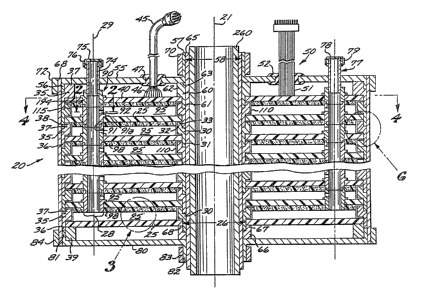
Re erring now to FIG. 9, another embodiment of a
card assembly embodying the invention is shown. This
~5 embodiment is particularly adapted to applications wherein
the circuit card assembly will be subjected to extremely
high "G" forces, e.g~, in exce~s of 100,000 G's. Assembly
150 comprises a plurality of ceramic circuit cards 155 and
ceramic spacer cards 160. The circuit cards 160 are
populated on one side with a plurality o~ electrical
components 156. The spacer card 160 ad~acent ~he popu-
lated surface of the circuit card 155 includes cutout
openings 161 which match the size and location of the
electrical components 156 on the circuit card 155 so that
the respective cards 155 and 160 fit together in intimate
, .... ..
,,. . , ,. .,:
:
" ", . :: ,.
~Q~3
1 contact. Each of the populated circuit cards 155 is
matched with a corresponding spacer card 160. Each
circuit card 155 and spacer card 160 is formed with a
central opening 157, 162 formed therein.
Each ceramic card 155 may comprise a ceramic sub-
strate layer with thin film multilayer interconnections.
Each card 155 and the spacer cards are interconnected by
the feedthrough contacts 165 fitted through holes formed
in the inner and outer periphery of the respective cards.
FIG. 10 shows a breakaway view of the periphery of a
circuit card 155 illustrating an exemplary feedthrough
165.
External electrical connection is made to the
assembly 150 via flat ribbon cables 180 and 182. The
individual conductive lines comprising the cables 180 and
18~ are in turn coupled to respective ones of the feed
through elements of the end cards 164, 165 comprising the
assembly 150. The cables 180, 18~ are respectively
connected to flat, flexible connector sheets 185, 187
~earing a conductive lead pattern, which are respectively
disposed between the termination plates 190, 191 and the
end cards 164 and 167 such that conductive pads on ~he
inner and outer peripheries of the layer contact the
respective feedthrough elements disposed around the
~5 adjacent peripheral edges.
Connector sheet 185 is shown in fur~her detail in
FIGS. 11 and 12. The outer peripheral configuration o~
the sheet 185 is circular to match that of the cards 155
and spacers 160. The sheet comprises first and second
layers 185a, 185b of flexible in~ulating material, such as
polymide film, which sandwich copper conductive traces
185c. The layer 185a is relieved at areas around the
outer periphery to allow the respective traces 185c to be
soldered to corresponding feedthrough eIement~ 165a of the
adjacent spacer card 160a. Thus, corresponding ones of
.
.. ... . ... . .
.:~.. - ::. : : . . ..
;: . :: ~. ,.: :
~27~3
1 the traces 185c are electrically connected to the feed-
through elements 165a to provide electrical connection to
the unit 150.
The termination plates 190 and 191 comprise moly-
bdenum compression plates fit~ed at the ends of the card
and spacer stack. A plurality of high tensile strength
bolts 175 are inserted throu~h aligned openings formed in
each of the circuit cards 155 and spacers 160, and are
sacured by fasteners 177. The fasteners are tightened
down so as to exert a high compression preload force on
the respective end plates, which is transmitted through to
compress the cards 155 and SpaGerS 160. The p~eload force
exerted on the assembly 150 by the fastener elements 175,
177 is as high or higher than the deceleration force
applied to ~he cards during operation so that the cards do
not experience any tensile forces. The ceramic substrates
comprising thè cards 155 and the spacers 160 are brittle
and might crack or break as a result of any applied
tensile forces.
~0 As the assembly 150 is brought into compression by
the fasteners, the aligned feedthrough elements 165 of
adjacent cards 155 and spacers 160 are brought into
contact, thereby making electrical connection. FIG. 13
illustrates in perspective view the fully assembled unit
150. As described with respect to the embodiment of FIGS.
1-8, the feedthrough elements 165 may pass directly
through the cards 155, or may make intermsdiate connection
to one or more of the multiple layers in a par~icular card
155. The feedthrough elements for the spac~rs 160 will
typically comprise direct feedthrough elements. As with
the embodiment of FIGS. 1-8, connector elements are
provided adjacent the outer periphery of the cards 155 and
spacers 160 and the inner peripheral edge as well. Thus,
separation between power lines and signal lines may be
achieved with this em~odiment as well.
:. ~ ,, . ~, .
-. ,. . ...: . .. ..::
: ,.. : :
,,3
1 Reerring now to FIGS. 14-17, another circuit
configuration embodying the invention is disclosed. As
with the embodiments already described, assembly 200
comprises a plurality of stacked circular circuit cards
205 each having a center opening 206 formed therein in
alignment with the center axis 201 of ~he unit. A pair of
outer support rings 216 and 217 is provided for each
circuit card 205 to provide support for ~he outer periph-
eral edge~ of the card. An inner support ring 220 is
provided to support the inner peripheral edge adjacent the
opening 206 in the card. The inner and outer support
rings are adapted to nest together wi~h corresponding
adjacent rings in ~he card stack.
In the embodiment of FIGS. 14-17, electrical con-
tinuity between adjacent caxds is achieved by the conduc-
tive paths applied directly ~o the inner and outer support
rings 216, 217 and 220~ The conduc~ive paths may be
applied by electrodeposition on the insulative material
comprising the rings, or by other suitable technique well
known in the circuit industry. The conductive paths
comprise a plurality of fine lines extending generally in
alignment with the central axis of the asse~bly. The
conductive paths make contact with conductive pads formed
on the inner and outer peripheries of the circuit cards,
as described with respect to the embodiment shown in FIGS.
l-8, once the card stack is fully assembled.
~IG. 16 is an exploded cross-sectional view of the
outer edge of a caxd 205 and the associated pairs of outer
rings 216a, 217a and 216b, 217b. This view depicts card
205 as having conductive traces or pads formed on the
upper and lower surfacec thereo~. Thus, conductive trace
211 is formed on the upper surface of the card 205, and
trace 212 is formed on the lower side of the card.
Corresponding traces axe ~ormed in the respective rings
216a, 217a, 216b, 2~7b and are aligned with corresponding
...: .:: " , ~ - ~
~: ' ,;,;` ''.:' , , .
6~
24
1 ones of the card traces to achieve electrical contact.
The upper rings 216a and 217a are secured to card 205 by
soldering at the respective junctures of the conductive
traces on the card 205 and the rings. The corresponding
inner ring 220 (not shown in FIG. 16) is also secured to
the card 205 to form the assembly layer 215 depicted in
FIG. 15. As shown in FIG. 16, the card edge is formed
with downwardly extending pointed ridges 208, 207 which
dovetail with V-shaped grooves formed in the rings 216b
10and 217b. A feedthrough 211a electrically connects a
~race formed on the V~shaped groo~e of ring 216b to
conductive trace 211 on the top of card 205. A trace
formed on ~he V-shaped groove of ring 217b connects with
trace 212 on the lower side of card 205.
15The card 205 may employ multilayer circuit board
technology. Moreover, the cards 205 may be fabricated
from materials such as a high tensile modulus graphite
epoxy composite for high strength. Two outer rings 216,
217 are shown to provide an increased number of circuit
connections over ~hose available if only a single outer
ring were employed.
FIG. 17 illustrates in cross-section typical cards
205a and 205b in the stacking configuration with inner
rings 220a, 220b and 220c. As with the outer rings 216,
~S 217, conductive traces are ormed on the inner rings 220
and are brought into contact with corresponding ~races on
the cards 205a, 205b and the adjacent rings.
The signal lines and power lines for this third
embodiment may also be separated with the inter-card power
connections made by power lines arranged along the inner
rings 220, and the inter-card signal connections mad~ by
signal lines arranged along the two outer rings 216, 217.
The number of ring-~, either~at the inner or outer periph-
ery of the cards, are determined according to the number
of interconnections required for the particular
.
, .: . ,, .. ,, :
, ., - ,~
1 application and may vary from layer to layer within a
particular assembly. For example, in a missile electron-
ics unit, the number of outer rings carrying the signal
linas may be increased for the computer card, the memory
card and the input/output cards because of the large
number of interconnections between these cards. Other
cards in the assembly requiring fewer interconnections
would have fewer rings.
The outermost ring in the assembly could also be
used, again for a missile application, to provide inter-
connections between the front and the aft end of the
electronics unit. These interconnections collld be sep-
arated from or connected to the cards in the unit as
required.
The outer rings comprise semicircular interlocking
regions 230 which key the relative rotational position of
the cards, allowing a simple means for proper integration
of the various cards into a completed assembly.
A novel circuit card configuration has been dis-
closed. The advantages of the new confiyuration includethe followin~:
1. Elimination of standard pin connectors reduces
the assembly and integration time of the unit as well as
the cost.
~5 2. The configuration lends itself to automated or
robotic assembly and testinq which should significantly
reduce assembly and testing costs.
3. The use of light weight materials for the spacer
elements, such as polymer/fiber composites, provides an
assembly whose strength and stiffness is several times
that of steel while weighing up to one-third less than
steel. These attributes of polymer/fiber composite
materials are particularly important advantages when the
assembly is to be used in a high G application.
.:
. - , :." :;,, : ". ' : ,. . .
. ~: :, .: : .:. . . . :
- . :,: ... : :
: ,
:; ~
~27~
1 4. Each card can be keyed for correct interfacing
to the next card, allowing a simple mean~ for integration
of the various cards into a completed assembly.
5. The cards can be tested individually or in any
sequential combination since all electxical lines are
readily accessible.
6. Separation of the power and signal lines should
improve isolation and reduce crosstalk between signals and
power~
7. The location of the power lines at the center
of the cards and the signal lines on the outside edges of
the circuit card provides an improvemen~ in the layout and
partitioning of the electrical components on ~he card.
Additionally, input and output signal lines could be
separated to further improve the isolation between sig-
nals, since these signal lines are not confined to partic-
ular areas as is the case when using standard pin connec-
tors.
The circuit card configurations described above are
advantageously used as guidance electronics units for
guided vehicles r such as missiles, torpedos or re-entry
vehicles. The card configurations may be employed with
the novel vehicle configuration shown in FIGS~ 18 and 19.
For purposes of illustration, FIGS~ 18 an~ 19 depict
a gu~ded missile configuration. It is to be understood
that this facet of the invention is not limited to mis-
siles, but is in general applicable to guided vehicles,
including guided missiles, torpedos, re-entry vehicles and
the like.
The missile 250 comprises the aft missile body 255,
carrying, for example, the missile propelling apparatus.
Extending forwardly along the central axi~252 of body 255
is a central tubular support element 260.
The guidance electronics unit 265 preerably com-
prises one of the circuit card configurations described
.-,.
,- . ; .
:: " ,. : .
~2~ 3
27
1 hereinabova with respect to FIGS. 1 17~ and is assembled
with the tubular element 260 extending through the central
opening formed in the unit 265. By way of example, the
tubular member 260 is also shown in FIG. 1 in the inser~ed
position. Tubular ou~er structural member 275 is fitted
about the unit 265 to form the forward outer missile body.
A sensor assembly 280 is secured to ~he tubular
element 260 and comprises a radome structure 295, a
re1ector dish 290, and a dish platform 285. The dish
platform 285 comprises a centxal opening 286 which
receives the tubular member 260. A fastener 262 is
threadingly received on tubular member 260 to secure the
platform 285 in compression against the body 275, unit 265
and aft body 255. The dish 290 and radome 295 are secured
to the platform 285. As will be apparent to those skilled
in the art, the reflector dish 290 is conventionally
coupled to the platform 285 by a gimball arrangement (not
shown) to allow movement of the reflector in relation to
the platform 285.
The missile configuration shown in FIGS. 18 and 19
further includes a means for keying the rotational align-
ment of various elements of the missile as it is assem-
bled. This means comprises the protruding regions 277 and
287 fo~med in the respective outer cover member 275 and
the platform 285, which regions engage in corresponding
relieved areas 257 and 276 formed in the outer surface of
the aft missile body 255 and the outer cover element 275.
As the various elements of the missile are assembled, the
elements are rotationally aligned to allow regions 277 and
287 to engage in areas 257 and 276.
The missile configuration shown in FIG. 18 solves
the problem of alignment of the platform 285 with the
surface 256 comprising the aft body 255. In order to
achieve accurate guidance of the missile, the boresight of
the sensor platform 285 is conventionally aligned in a
:-. ~: ,.
:: .
. ~ : ., . :
:; . ~ ~ ..... . :
. , ; ,.. .. ..
. ,, ,:, ,~,, :.. : :
, : :- : ::: ~:- .: - ,.
~Z~6~
28
1 predetermined relationship with the aft body 255. Typi-
cally, the alignment may comprise securing the platform
285 such that i~ is in exact parallel alignment with
planar surface 256 of the aft body. The alignment is
provided very simply with the disclosed configuration, by
tighteniny down the fastener 262 to secure the various
elements shown in FIG. 18.
The platform 285 abuts the adjacent forward end of
the cover 275, with the af~i end of the cover abutting
1~ surface 256, as the fastener is secured. As the elements
255, 265, 275 and 285 are brought together by the com-
pression forces of the fastener on the forward end and the
surface 256 on the aft end, the alignment of the plane
defined by the platform 285 will be determined by the
alignment of the ends of the tubular structural member
275. If the respective ends of the member 275 define
planes perpendicularly intersecting the center axis 252,
then the platform 285 will be aligned with the plane 25~
of the aft body. As will be appreciated by those skilled
in the art, for certain applications it may be desirable
to reverse the configuration of FIG. 18, such that the
tubular support member extends from a forward section of
the vehicle toward the aft portion of the vehicle.
The tubular outer structural member 275 is suffic-
iently rigid so a~ to provide an outer cover, as well as
to withstand the compression forces exerted by the opera-
tion of the fastener 262. The members 260 and 265 are
subjected to tension and compression preload forces which
are sufficient to withstand any operational stresses
encountered during missile ~light.
It is under~tood that the above-described embodiment
is merely illustrative of the possible specific embodi-
ments which may represent principles o~ the present
invention. Other arrangements may be devised in accor-
dance with these principles by those skilled in the art
without departing from the scope of the invention~
": ~ : :
; ::: . , ; .
. :,:: . :
:: .."~
; ,i" ~ . . ,
~. :