Note: Descriptions are shown in the official language in which they were submitted.
~ ~7~l~3fl~
20104-~161
Field-programmable logic device with programmable foldback to
control number of logic levels.
Fiel~_of Use
This invention relates generally to digital integrated
circuits and, in particular~ to programmable logic devices.
Back~round Ar~
Programmable logic devices have become popular in the
electronics industry because they allow the manufacturer and use~
flexibility in tailoring a general integrated circuit to meet
specific applications at low cost. Programmable logic devices are
generally classified as field-programmable and mask-programmable.
In contrast to a mask-programmable logic devices which the
manufacturer programs late in the fabrication process and then
distributes to the customer, a field-programmable logic device
(hereafter generally "PLD") is typically distributed in an
unprogrammed state. The customer subsequently programs the PLD to
perform a desired logic function.
Logical operations in PLD's are performed with arrays of
basic logic gates having programmable elements at selected points.
The most common type of programmable element is a fusible link or
fuse. A PLD is programmed to imbed a particular function in the
device by destroying (or "blowing") a speclfic pattern of the
fuses. Blowing a fuse creates an open circuit at a location where
an electrical connec~ion is not wanted. Conversely, a closed
circuit exists at a crosspoint where the fuse remalns intact to
provide an electrical connection. Another type of programmable
element is the so-called "antifuse". In contrast to a fuse, an
3~
20104-8161
antifuse is initially an open circuit and is programmed to create
a closed circuit where an electrical connection is desired.
Brief Description of the Drawin~s
Figures la, lb, and lc respectively show a circuit
diagram for a conventional programmable NAND gate, its standard
logic representation, and its representation in a simplified PLD
notation.
Figures 2a, 2b and 2c respectively show a circuit
diagram for a conventional programmable NOR gate, i~s standard
logic representation, and its representation in th~ simplified PLD
notation.
Figures ~a and 3b are circuit diagrams respectively
representing two prior art PLD's.
Figures 4 and 5 are circuit diagrams for basic PLD's
that respectively use NAND and NOR arrays with foldback in
accordance with the invention.
Figure 6 is a circuit/block diagram for a mulki-
capability PLD using the NAND core of Figure 4.
Figures 7 and 8 are circuit diagrams for particular
embodiments of the PLD of Figure 6.
Like reference symbols are employed in the drawinys and
in the description of the preferred embodiments to represent the
same or very similar item or items. Reference symbols beginning
with "I" and "O" respectively indicate circult input and output
pins. Reference symbols beginning with "V" indicate signals that
are not necessarily transmitted at the input and output pins.
Each circled intersection in which the vertical
la
7~3'~
2010~~8161
(crossinq) line is connected ~o ground refe~ence but which is
located outside the array(s) of programmable gates indicates a
programmable element. By suitably programming this element, the
horizon~al (crossing) line is either grounded at logical "O" or
left as an open circuit at logical "1".
Turning to the drawings, Figure la illustrates ~he
internal construction of a conventional unprogrammed loglcal NAND
gate C suitable for a PLD using fuses as the programmable
elements. Digital input data consisting of N input signals VIl-
VIN is provided from primary lines Ll-LN to N corresponding input
sections of gate C. Letting J be a running integer, each gate
input section consists of a Schottky diode DJ connected by way of
a gate input line SJ to primary line LJ. A fuse FcJ couples line
SJ (and diode DJ) in the input section to a line Sc in the output
~ection
lb
~ ~7~3'~
~.
PHA 1136 2 28-08-1986
of gate C. An inverter NC connected to line Sc supplies the gate out-
put signal VO.
Programming involves destroying certain of fuses FC1-FCN to dis-
connect the corresponding input sections of gate C from its cutput
sections. Signal VO then hecomes the logical NAND of only those of
signals VI1-VIN associated with the fuses that are still intact.
Fig. lb represents gate C in standard logic notation. This nota-
tion is inconvenient for PLD's. The simplified notation of Fig.lc
alleviates this problem. In Fig. 1c, line Sc in the output section
crosses each line LJ perpendicularly. Each of the resulting inter-
sections represents the unprogrammed location for a potential coupling
of line Sc to line LJ through fuse FcJ (and diode DJ) as shown in
Fig. 1a. Each unprogrammed intersection is marked with a small circle to
distinguish intersections for programmable elements from other circuit
intersections not intended to represent programmab]e elements. The NAND
symbol (which encompasses only the gate output section here) is placed
at a suitable location along line Sc to indicate the function of the
circuitry. The same notation would be used in Fig. 1c if the programmr
able element were an antifuse instead of a fuse.
Figs. 2a, 2b, and 2c respective]y show the internal circuitry of
a conventional unprogrammed logical NOR gate E, its representation in
standard logic notation, a~d its representation in the simplified nota-
tion described above. As with gate C, signals VI1-VIN are provided from
input lines I.1-LN to N input sections of ga-te E. Each input section
consists of an NPN transistor QJ whose hase is connected via a gate in-
put line SJ to line LJ as indicated in Fig. 2a. A fuse FEJ connects the
QJ emitter to a line SE in the gate output section. Gate output signal
VO is provided from an inverter NE connected to line SE.
Gate E is utilized in the same t~ay as yate C. Selectively blowing
fuses FE1-FEN causes signal VO to become the logical NOR of only those
of signals VI1-VIN whose fuses remain intact. Likewisel the simplified
notation of Fig. 2c is more appropriate to PLD's than the standard
notation of Fig. 2b. Each circled intersection in Fig. 2c represents
the unprogrammed location for a potential coupling of line SE to line
I,J through fuse FEJ.
The preceding remarks also apply to loyical AND and loyical OR
gates- Replacing inverter NC in gate C t~ith a non-inverting buffer
(or simply taking the output siynal directly from line Sc) transforms
iL27~
,-
" PHA 1136 3 28-08-1986
the gate into a programmable AND gate. The same thing can be done
with gate E to convert it into an OR gate.
It is difficult to adjust the nun~er of basic (or Boolean) logic
levels in prior art PLD's. Many simply have fixed numbers of logic
leve]s. Typical of the fixed-level PLD's are the 82S100, 82S103, and
82S105 integrated circuits made by Signetics Corporation. The 82S100 and
82S105 have tw~ levels of Boolean logic. The 82S103 is a single-level
device.
Fig. 3a shows the architecture for the 82S100. Circuit input data
is transmitted through M input pins I1-IM to complementary-output
buffers W1-WM which supply the true input data and its complement to
array input lines L1L2M. An array of P programmable AND gates A1-A~
ANDs the data on lines L1-L2M to provide a first level of logic as
Boolean products. m e second level of logic is to form sums of the
products. m is is done with a array of Q programmable OR gates E1-EQ
that OR the data fr~n gates A1-Ap. EXCI,USIVE OR gates X1~XQ selectively
invert the ORed data. The resulting data is supplied through buffexs
B1-BQ, whose activation can ke externally controlled, to output pins
1-Q-
The 82S103 is similar to the 82S100 except that the 82S103 does not
have the OR logic level. Also, the AND array is replaced with an array
of programmable N~ND gates, each arranged as descriked in Fig. 1a. The
NAND gates are directly connected to the EXCLUSIVE O~ gates~
Fig. 3b shows the basic building blocks of the 82S105. In this
simplified representation, gates A1-Ap AND the data on input lines
L1-L2M and on typical feedback lines LE1, LE2, and LN. The ANDed data
is supplied to typical gates E1-E4 and EN in a programmable OR array.
SR flip-flops FF1 and FF2 provide on-chip data storage. Their data in-
puts accept the ORed data from gates E1-E4 in synchronism with a clock
signal VcK. The flip-flop states can be set asynchronously to logical "l"
through a preset signal Vp. The FFl cutput data is fed back to the AND
array. The FF2 Outplt data is supplied via an extexnally controllable
buffer BF to a pin OF. The 82S105 also has a (single) programmable NOR
loop for feeding data complementary to that supplied from gates A1-Ap
back into them. The NOR loop is formed with an inverter NN connected
betwee~ line l~ and gate EN.
U.S. Patent 4,422,072 describes more advanced versions of the fore-
going Signetics PLD-s. These more advanced versions offer significantly
7~
2010~-~161
more archikectural flexlbility. To a certain degree, they can be
programmed to achieve different numbers of basic logic levels.
Since they are basically directed toward fixed-level usage, this
ls a relatively tortuous process which entails sacrific:lng æome of
their internal logic resources, package pins, and performance.
General Disclosure of the Invention
The present invention provides a programmable logic
archi~ecture centered on a sinyle programmable loyic array that
the user can readily configure in foldback loops to achieve
different number of Boolean logic levels within a single
integrated circuit. This provides a great increase in usage
efficiency. The array typically serves as a highly flexible
central interconnect system for coupling peripheral logic elements
of various complexity.
According to a broad aspect of the invention there is
provided a monolithic integrated programmable logic device having,
a plurality of pr~mary lines, at least part of which are input
linas for receiving external input data; an array of primary logic
gates, each gate having ~1) a plurality of input sections of which
each is connected to a different ona of the primary lines and ~2)
an output section for providing an output signal as either the
logical NAND or the loglcal NOR of the input data to that gate;
and means for selectively programmably connecting each input
section of each gate to its output sectlon; characteri7ed in that
at least part of the gates are foldback gates whose output
sections are respectively connected to corresponding foldback
lines consisting of part of the primary lines exclusive of the
~L~t~
20104-816~
input lines, whereby each foldback line receives the output signal
from the corresponding foldback gate.
According to anothex broad aspect of the invention thsre
is pxovided a monoli~hic integrated programmable logic device
formed as an integrated circuit having pins for recelvlng device
input data and supplying device output data, the device
comprising:
input means for performlng at least one digital operation on
at least a portion of the device input data to generate internal
0 input data;
a plurality of primary lines, part of which are input lines
for receiving at least a portion of the lnternal input data and
part of which are foldback lines;
an array of primary logic gates, each gate having (1) a
plurality of input sections of which each is connected to a
different one of the primary lines and (2) an output section for
providing an output signal as either the logical NAN~ or the
logical NOR of the input data to that gate, at least part of the
gates being foldback gates respectively corresponding to the
foldback lines, the output section of each foldback gate connected
to the corresponding foldback line so that it receives the output
signal from that f oldback gate;
means for selectively programmably connecting each input
section of each primary gate to its output section; and
output means for performing at least one digital opera~ion on
the output signal from at least one of the gates to generate at
least a poxtion of the device output data.
4a
20104-8161
Insofar as the texm "programmably connecting" and
similar terms are used herein, these terms are intended to mean
both the situation where the pxogrammable elements are initially
closed circuits that are opened during progxamming and the
situation in which the programmable elements are initially open
circuit~ that are closed during programming. That is,
"programmably connecting" covers both fuses and antifuses.
Configuring the present logic device to obtain various
numbers of logic levels simply involves programming the
programmable elements located in the array of ga~e~ i~self. No
other elements need to be programmed.
Consider the preferred case in which all the gates are
NAND gates. According to DeMorgan's theorem, an NAND gate with
inverted inputs functions as an OR gate. If a gate in the present
array is programmed
~3 4b
1.~27~3~
20104-8161
to connect its output section to a pair of its inpu-t sections
connected to foldback lines, the resulting foldback lovp through
that gate and the corresponding pair of foldback gates yields two
levels of NAND logic. These are equivalen~ to a level of AND
logic followed by a level of OR logic. More than two logic levels
can be attained by programming further foldback loops through the
array. An important feature of the invention is that different
input-to-output paths through the device can be programmed to
have different numbers of basic logic levels. This makes the
invention very adaptable.
DescriPtion of the Preferred Embodiments
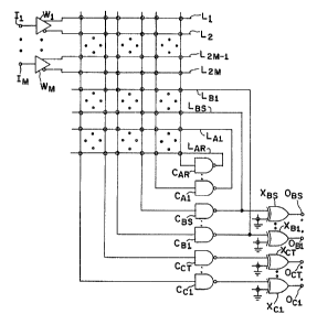
Figure 4 illustrates a single-chip NAND-based field-
programmable logic device with foldback that can be programmed to
achieve different
~7 ~ ;3~
PHA 1136 6 28-0~-1986
numbers of leve]s of logic. m is PLD has a group of primary lines
consisting of 2M array input lines L1-L2M, R foldback lines I,A1-LAR,
and S foldback lines LB1-LBS. Input data to the integrated circuit is
transmitted from input pins I1-IM to respective complementary-output
buffers W1-WM which provides the true input data and its complement
to input lines L1-L2M.
The PID has an array of programmable N~ND gates whose input sec-
tions are respectively connected to lines Ll-L2M, LA1-LAR, and LB1-LBS.
Each NAND gate is configured (for example) as shown in Fig. 1a using
fuses for programming. One part of the NAND array consists of R fold-
back gates CA1-CAR whose output sections respectively provide their
output signals directly to lines LA1-LAR. Another par-t of the array
consists of S foldback gates CB1-CBs whose output sections are similarly
connected respectively to lines LB1-LBS.
In programming this PLD, the fuses connecting the output sections
of each gate CAJ or CBJ (where J is a running integer) to the input
section connected to its foldback line I.AJ or LBJ must ke blown to
create open circuits. mis is done to avoid oscillations. Alternatively,
these particular fuses could simply be deleted in fabricating the array.
me programmable array also includes T gates Cc1-CCT. The NPND
output signals from gates CB1-CBs and Cc1-CCT are respectively provided
to the first inputs of S EXCLUSIVE OR gates ~ S and T EXCLUSIVE OR
gates Xc1-XcT. The second inputs of gates XB1-XBS and XC1-~cT are pro-
gra~mably groundable to enable output data from gates CB1~CBs and Cc1-
CcT to ke selectively inverted. The elements that provide the pro-
grammable grounding are implementated (for example) in the way described
in U.S. Patent 4,422,072, cited a~ove. The output signals from gates
XB1-XE~ and Xc1-XCT are respectively supplied to S output pins 0~1-OBs
and T output pins OC1-0cT
The PLD has a limited numker of pins. Consequently, R is normally
chosen to be much higher than S so as to maximize pin usage efficiency.
Various numbers of Boolean logic levels can be obtained in the
PLD by configuring suitable foldback loops throuah the N~ND array. A
foldback loop is created by programming the array in such a manner that
there are complete electrica] paths extending from two or m~re of the
input sections of each of tw~ or more of the foldback gates -- e.g.,
gates CA1 and CA2 -- through their output sections and along their
PHA 1136 7 28-08-1986
foldback lines -- i e.., lines LAl and LA2 here -- to the output section
of another of the gates -- e.g., gate &1 --- by way of its input
sections connected to those foldback lines.
Specifically, the Cc1 fuses "along" -- i.e., connected to the
gate input sections connected to -- lines LA1 and LA2 are allowed to
remain intact. If the user wants gate CA1 to respond to input data at
pins I1-IM, two or more of the CA1 fuses "along" lines L1-L2M are
allowed to remain intact, subject to the proviso that the CAl fuse(s)
"along" at least one of the two lines extending from the outputs of
each of buffers W1-WM must be blown. The same applied to gate CA2 if
the user wants it to respond to pin input data.
The result is that gates CA1 and CA2 receive array input data from
certain of lines L1-L2M to provide a first level of NAND logic. The
output signals from gates CA1 and CA2 are supplied as input signals to
gate Cc1 to obtain a second NAND logic level. The foldback loop formed
with gates CA1, CA2, and ~A1 thereby gives a t~o-level NAND-NAND arrange-
ment.
A NAND gate is functionally and AND gate with output inversion.
Gates CA1 and CA2 theref~re are AND gates with inverters at their out-
puts. These inverters can be functionally shifted to the Cc1 inputs.
Under DeMorgan's theorem, a NAND gate with inverted inputs performs an
OR function. Accordingly, the NAND-NAND arrangement formed with gates
CA1, CA2, and Cc2 is functionally equivalent to a two-level AND-OR
structure. This gives the standard Boolean sum of products.
2s By slightly altering the preceding foldb~ck loop, it can ke placed
in series with one or more additional foldback loops to achieve three
or more leve]s of logic. In particular, the array could be programmed so
that foldback gates CA1 and CA2 receive input data from other foldback
gates by way of their foldback lines instead of solely from lines L1~L2M
A three-level arrangement is a NAND-NAND-NAND structure which is func-
tionally equivalent to an AND-OR-NAND structure (or to a NPND-AND-OR
structure). Similarly, a four-level arrangement is a NAND-NAND-NAND-NAND
structure functionally equivalent to an AND-OR-AND~OR structure~ Of
course, a single level of NAND logic is obtained by simply not programm-
ing any foldback loop along and input-to-~utput path through the PLD.
Importantly, different numkers of Boolean logic levels can exist
on different input-to-output paths through the PLD. It can thus ke
readily adapted to a large variety of applications.
~L~7~;3~
PHA 1136 8 28-08-1986
Returning momentarily to gates CB1-CBs, they provide more
f~exibility. They are generally interchangeable with foldkack gates
CAl-CAR and non-fo]dback gates Cc1-CCT. Also, gates CB1-CBs can ke
used to supply output data at intermediate logic levels.
Moving to Fig. 5, it illustrates the building blocks of a NOR-
based PLD in which foldback loops can ke program~ed to achieve different
numbers of logic levels. The PLD has K input lines L1-LK that receive
array input data and a group of foldback lines of which t~ such lines
LA and LB are shown. m e core of this PLD is an array of programmable
NOR gates, of which gates EA, EB, and EC are typical. Each NOR gate is
configures (for example) as shown in Fig. 2a. Gates EA and EB are
foldback gates whose cutput sections are respectively connected to lines
LA and LB. The gates have input sections respectively connected to lines
L1-LK and to the foldkack lines except that gates EA and EB are shown
here as not having input sections connected respectively to lines L~
and LB since the associated fuses, if present, would have to ke destroyed
during programming to prevent oscillations. Gates EB and EC provide
array output data.
The PLD of Fig. 5 is utilized in the same way as that of Fig. 4r
Programming this NOR-based PID in the manner generally descrikecl above
for Fig. 4 yields one or m~re levels of NOR logic. A NOR gate with
inverted inputs performs an AND function under DeMDrgan's thRorem. For
the tw~-level case, the resulting NOR-NOR structure is functionally
equivalent to and OR-AND arrangement. This gives a Boolean product of
sums.
The basic NAND array with foldback in Fig. 4 serves as a central
interconnect system for a more complex single-chip PLD whose building
blocXs are illustrated in Fig. 6. Normally, there are tWD or ~ore of
each of the elements indicated in~Fig. 6. Each of the lines leading to
and from the various "DEVIOE " blocks may also be two or more lines.
With the ~oregoing in mind, the main programmable array consists
of NAND gates CA-CF. On a relative scale, the PLD normally has a large
number of foldback gates CA, CB, and CD so as to maximize usage
efficiency.
Input devices 11 and 12 perform logical operations on input data
received at pins I and IOF of the integrated circuit and provide the
resulting data to the NAND array on lines I1 L3. Output devices 13, 14,
~.~7~3~
PHA 1136 9 28-08-1986
and 15 perform logical operations on the output data from gates
CB, Cc, and CF and supply the resulting data to pins OB~ & ~ and
IOF. Internal devices 16 ad 17 perform logical operations on the data
from gates CD and CE and provide the resulting data back to the array.
Devices 11 - 17 can take many forms including inverters, non-inverting
buffers, complementary-~utput buffers, flip-flops, EXCLUSIVE OR gates,
counters, registers, multiplexers, decoders, arithmetic ]ogic units, and
memories.
The basic advantage of this configuration lies in merging into a
single programmable core both "interconnect" and "logic transform" ele-
ments required to interlace peripheral on-chip devices (or macros) into
a functional whole performing a specific logic algorithm. The core can,
in turn, be fragmented and distributed in an unprecedented way to
maximize the efficient implementation of each signal path linking
individual logic macros on chip.
Fig. 7 shows a preferred embodiment of the PID of Fig. 6. The
integrated circuit in Fig. 7 is implementated with antifuses. In view
of the preceding material, much of Fig. 7 is self-explanatory. Accord-
ingly, only a brief discussion is given here of this preferred e~odiment.
Devices 11 and 12 are complementary-output buffers W1 and W2. In
device 15, a buffer BF1 controls transmission of the CF output signal
to pin IOF. The activation of buffer BF1 is controlled by a signal
from the output of a buffer BF2 whose input is programmably groundable.
Permanently enabling buffer BF1 makes pin IOF an output pin and allows
the CF output data to be fed back to buffer W2; the user shou]d not
attempt to employ pin IOF as an input pin. Conversely, disabl~ng buffer
BF1 fixes pin IOF as an input pin. Buffer BF1 is enabled when the BF2
output signal is logical "1", and vice versa.
Output devices 141 and 142 a~e employed with gate Cc1-Cc5 of the
NAND array. Device 141 permits or inhibits transmission of the Cc1
output data to a pin C1 as a function of the & 2 output data. This is
done with a buffer BC1 which lies in the Cc1 output signal path and whose
activation is controlled by the Cc2 output signal. Device 142 similarly
controls transmission of the EXCLUSIVE OR of the Cc3 and Cc4 output
data to a pin C2 To perform this function, a gate Xcl generates the
EXCLUSIVE OR of the Cc3 and Cc4 output signals. A buffer BC2, whose
activation is under control of the Cc5 output signal, controls trans-
1~7~3'~
.~
PHA 1136 10 28-08-1986
mission of the Xc1 output data to pin & 2 Buffers BC1 and BC2 are
enabled when the respective output signals from gates Cc2 and Cc5 are
logical "O", and vice versa.
The PLD of Fig. 7 preferably has 80 gates CA. This provides an
extensive foldback capability. There are 24 devices 11. The PLD has 8
combinations of devices 12 and 15. The PLD also contains 4 devices
141, 4 devices of the same type in which buffer BC1 is replaced with an
inverter, and 8 devices 142.
Fig. 8 illustrates another preferred emkodiment of Fig. 6. This
integrated circuit is implemented with fuses. Only a brief discussion
is given here of Fig. 8 since much of it is self-explanatory.
NAND gates Cc6 and Cc7 are employed with an output device 143.
It controls transmission of either the Cc6 true output data or its
inverse as a function of the Cc7 output signal. This is accomplished
with a gate Xc2 that generates the FXCLUSIVE OR of the inverse of the
Cc6 output signal and another signal which is progra~mably either logical
"O" or "1". A buffer Bc3~ whose activation is controlled by the Cc7
output signal, controls transmission of the Xc2 output signal to pin
O~3. Buffer Bc3 is enabled ~hen CcT output signal is logical "O", and
vice versa.
NAND gates CE1-CE7 are used with internal devices 171-173 to pro-
vide on-chip data storage. Device 171 consists of a D-type flip-flop
FE1 which supplies its true and complementary output signals on lines
LE1 and LE2 in response to a data input signal from gate CE1 in syn-
chronism with a clock signal. Device 172 consists of an SR flip-flop
FE2 which supplies its true and complementary output signals on lines
LE3 and LE4 in response to data input signals from gates CE3 and CE4 in
synchronism with a clock signal. Flip-flops FE1 and FE2 can ~e cleared
asynchronously to logical "O" in response to the respective output
signals from gates CF2 and CE5 Clearing occurs when the CE2 and CE5
output signals are logical "O", and vice versa.
Device 173 controls the clocking of flip-flops FE1 and FE2 with
an array of further progra~mable NAND gates CcK1 and CcK2 whose output
signals are the respective flip-flop clock signals. The input sections
of each gate CCK1 or CcK2 are respectively connected to clock lines
L -L and to lines LE1-LE4- Lines LCK1 LCK3 r p
the inverse of CE6 output signal, the CE7 output signal, and the inverse
- - ~
PHA 1136 11 28-08-19~6
of a clocking signal supplied at a pin ICK.
The PLD of Fig. 8 preferably contains 68 foldback gates CA. It
has 20 devices 11 and 8 ccmbinations 12/15. There are 4 devices 141, 4
like devices with output inversion, and 8 devices 143. The PLD also
5 has 8 devices 171 and 8 devices 172. There is only one gate CE2 or CE5
for controlling all 8 flip-flops FE1 or FE~. Device 173 contains 8 gates
CcK1, 8 gate5 CcK2, 4 NcK/W3 combinati~ns, 2 gates CE6 and 2 gates CE7
While the invention has been descri~ed with reference to particular
embodiments, this descriptio~ is solely for the purpose of illustration
and is not to be construed as limiting the scope of the invention claimed
below. For example, the positions of the diode and the fuse in each of
the input sections of the NAND gate of Fig. 1a could be reversed; each
input section would then consist only of the gate input line. The same
thing applied to Fig. 2a. The NPND and NOR gates could be lmpleme.nted
with elements other than diodes and bipolar transistors. EXCLUSIVE NOR
gates can generally be substituted for EXCLUSIVE OR gates. Progra~ming
could be done with masks. Thus, various modifications, changes, and
applications may be made by those skilled in the art without departing
from the true scope and spirit of the invention as defined by the appended
20 claims.